Fujitsu MB91150 Series Скачать руководство пользователя страница 471

455

APPENDIX C  Pin Status in Each CPU State

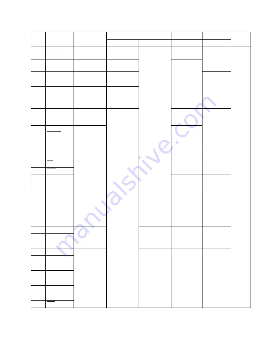
Table C-3  Pin status in external bus 8-bit mode

Pin 

name

Function

In sleep mode

In stop mode

Bus release

At reset

Remarks

HIZX=0

HIZX=1

(BGRNT=1)

(RST=1)

P20-7

Port

Last status 
retained

Last status 
retained

Output Hi-Z or 
keep the input at 
0

Last status 
retained

Output Hi-Z or 
enable all-pin 
input

-

P30-7

D24-31

Output retained 
or Hi-Z

Output retained 
or Hi-Z

Output Hi-Z

P40-7

A0-7

Output enabled
(Address output)

Output enabled
(Address output)

FF

output

P50-7

A8-15

P60-7

A16-23/

P: Last status 
retained
F: Address 
output

P: Last status 
retained
F: Address 
output

P80

RDY

P: Last status 
retained
F: RDY input

Output Hi-Z or 
keep the input at 
0

P: Last status 
retained
F: RDY input

Output Hi-Z or 
enable all-pin 
input

P81

BGRNT

P: Last status 
retained
F: H output

L output

P82

BRQ

P: Last status 
retained
F: BRQ input

BRQ input

P83

RD

Last status 
retained

Output Hi-Z

H output

P84

WR0

P85

Port

Last status 
retained

Output Hi-Z or 
enable all-pin 
input

P86

CLK

P: Last status 
retained
F: CLK output

CLK output

CLK output

PC0-3 INT0-3

Last status 
retained

Input enabled

Input enabled

Last status 
retained

Output Hi-Z or 
enable all-pin 
input

PC4

INT4/CS0

P: Last status 
retained
F: CS output

Output Hi-Z
Input enabled

Last status 
retained
Hi-Z for CS 
output

CS output

PC5-7 INT5-7/CS1-3

PD0

AIN0/INT8

Last status 
retained

Input enabled

Last status 
retained

Output Hi-Z or 
enable all-pin 
input

PD1

BIN0/INT9

PD2

AIN1/INT10

PD3

BIN1/INT11

PD4

ZIN0/INT12

PD5

ZIN1/INT13

PD6

DEOP2/INT14

PD7

ATG/INT15

Содержание MB91150 Series

Страница 1: ......

Страница 2: ......

Страница 3: ...FUJITSU LIMITED FR30 32 BIT MICROCONTROLLER MB91150 Series HARDWARE MANUAL ...

Страница 4: ......

Страница 5: ...eers who develop products incorporating the MB91150 It also describes the functions and operation of the MB91150 Read this manual thoroughly For details on each instruction see the Instructions Manual Trademarks FR is an abbreviation of FUJITSU RISC controller and a product of FUJITSU LIMITED Embedded AlgorithmTM is a trademark of Advanced Micro Device Corporation License Purchase of FUJITSU I2C c...

Страница 6: ...ram and the structures and functions of the timer registers CHAPTER 8 PPG TIMER This chapter describes the PPG timer It also describes the operations of the PPG timer block diagram and the structures and functions of the timer registers CHAPTER 9 MULTIFUNCTIONAL TIMER This chapter describes the multifunctional timer It also describes the operations of the multifunctional timer block diagram and th...

Страница 7: ...urces and DMAC timing The chapter also provides notes on using the DMAC CHAPTER 18 BIT SEARCH MODULE This chapter describes the bit search module It also describes the structures and functions of bit search module registers and the processing for saving and restoring CHAPTER 19 PERIPHERAL STOP CONTROL This chapter describes peripheral stop control and structures and functions of the registers CHAP...

Страница 8: ...ein The products described in this document are designed developed and manufactured as contemplated for general use including without limitation ordinary industrial use general office use personal use and household use but are not designed developed and manufactured as contemplated 1 for use accompanying fatal risks or dangers that unless extremely high safety is secured could have a serious effec...

Страница 9: ...enerator and an interrupt controller are connected to the R BUS The R BUS has a bandwidth of 16 bits over which addresses and data are multiplexed CPU access time of these resources is several cycles E unit Arithmetic execution unit φ System clock It provides the clock signals output to each of the built in resources connected to the R BUS from the clock generator The maximum clock speed cycle is ...

Страница 10: ...vi ...

Страница 11: ... Slot 52 3 8 EIT Exception Interrupt and Trap 53 3 8 1 Interrupt Level 54 3 8 2 Interrupt Stack Operation 55 3 8 3 EIT Vector Table 56 3 8 4 Multiple EIT Processing 58 3 8 5 EIT Operation 60 3 9 Reset Sequence 64 3 10 Operation Mode 65 3 11 Clock Generator Low Power Consumption Mechanism 67 3 11 1 Reset Source Register RSRR and Watchdog Cycle Control Register WTCR 69 3 11 2 Standby Control Registe...

Страница 12: ...ernal Access in Big endian and Little endian Mode 126 4 5 Bus Timing 131 4 5 1 Basic Read Cycle 132 4 5 2 Basic Write Cycle 134 4 5 3 Read Cycle in Each Mode 136 4 5 4 Write Cycle in Each Mode 138 4 5 5 Mixed Read Write Cycles 140 4 5 6 Automatic Wait Cycle 141 4 5 7 External Wait Cycle 142 4 5 8 External Bus Request 143 4 6 Internal Clock Multiply Operation Clock Doubler 144 4 7 Program Examples ...

Страница 13: ...er Operation States 197 CHAPTER 8 PPG TIMER 199 8 1 Overview of PPG Timer 200 8 2 Block Diagram of PPG Timer 201 8 3 Registers of PPG Timer 203 8 3 1 Control status registers PCNH PCNL 205 8 3 2 PWM cycle set register PCSR 209 8 3 3 PWM duty set register PDUT 210 8 3 4 PWM timer register PTWR 211 8 3 5 General control register 1 GCN1 212 8 3 6 General control register 2 GCN2 215 8 4 PWM Operation ...

Страница 14: ...ority Evaluation 267 12 5 Return from Standby Stop or Sleep Mode 269 12 6 Hold Request Cancellation Request 270 12 7 Example of Using Hold Request Cancellation Request Function HRCR 271 CHAPTER 13 8 10 BIT A D CONVERTER 275 13 1 Overview of the 8 10 bit A D Converter 276 13 2 8 10 bit A D Converter Block Diagram 277 13 3 8 10 bit A D Converter Pins 279 13 4 8 10 bit A D Converter Registers 281 13 ...

Страница 15: ...cessor mode 343 15 10 Notes on Using UART 345 CHAPTER 16 I2C INTERFACE 347 16 1 Overview of I2C Interface 348 16 2 Block Diagram of I2 C Interface 349 16 3 Registers of I2C Interface 350 16 3 1 Bus Control Register IBCR 351 16 3 2 Bus Status Register IBSR 354 16 3 3 Address Register IADR Data Register IDAR 356 16 3 4 Clock Control Register ICCR 357 16 4 Operation of I2 C Interface 359 CHAPTER 17 D...

Страница 16: ...r Macro Registers 407 20 3 Calendar Macro Operation 411 CHAPTER 21 FLASH MEMORY 413 21 1 Overview of Flash Memory 414 21 2 Flash Memory Registers 418 21 3 Flash Memory Operation 421 21 4 Automatic Algorithm of Flash Memory 423 21 5 Checking the Automatic Algorithm Execution Status 427 21 6 Writing and Erasing Flash Memory 432 21 6 1 Putting flash memory into read reset status 433 21 6 2 Writing da...

Страница 17: ...equired to fully understand the MB91150 such as a description of MB91150 features block diagrams and an outline of functions 1 1 MB91150 Features 1 2 Comprehensive Block Diagram of MB91150 1 3 Exterior Dimensions 1 4 Pin Assignment Drawing 1 5 Pin Functions 1 6 I O Circuit Types ...

Страница 18: ...sage Instructions for entry exit functions multiple load store instructions for the register contents instructions for high level languages Register interlock function allowing simpler assembler code Branch instruction with a delay slot allowing a decrease in overhead for branch processing Built in multiplier supported on the instruction level Signed 32 bit multiplication 5 cycles Signed 16 bit mu...

Страница 19: ...the first I O bit change starting with the MSB of a word Timer 16 bit OCU x 8 channels ICU x 4 channels free run timer x 1 channel 8 bit or 16 bit up down timer counter 8 bit x 2 channels or 16 bit x 1 channel The AIN and BIN pins are shared with internal interrupts 16 bit PPG timer x 6 channels The cycle and duty of an output pulse can be changed to an arbitrary value 16 bit reload timer x 4 chan...

Страница 20: ... I2 C patent of Philips Clock switching function The ratio of the operating clock to the base clock can independently be set with the gear function to 1 1 1 2 1 4 or 1 8 for the CPU and for each peripheral device Clock function calendar macro Built in 32 kHz clock function The 32 kHz oscillation clock function can operate in stop mode as well 32 kHz oscillation does not stop in stop mode Interrupt...

Страница 21: ...DMAC I Bus D Bus C Bus FR30 CPU Core I Bus D Bus MD0 MD1 MD2 RST M O D E 4 Data RAM 32KB PG2 PPG2 PG1 PPG1 PG0 PPG0 PPG PG5 PPG5 PG4 PPG4 PG3 PPG3 PJ0 SCL PJ1 SDA I2 C PE7 OC7 PE6 OC6 PE5 OC5 PE4 OC4 PE3 OC3 PE2 OC2 PE1 OC1 PE0 OC0 Output Compare TOX Reload Timer PH0 SIN0 PH1 SOT0 PH2 SCK0 T00 PH3 SIN1 PH4 SOT1 PH5 SCK1 T01 PI0 SIN2 PI1 SOT2 PI2 SCK2 T02 PI4 SOT3 PI5 SCK3 T03 PI3 SIN3 UART P37 D31...

Страница 22: ...PPG0 PPG PG5 PPG5 PG4 PPG4 PG3 PPG3 PJ0 SCL PJ1 SDA I2 C PE7 OC7 PE6 OC6 PE5 OC5 PE4 OC4 PE3 OC3 PE2 OC2 PE1 OC1 PE0 OC0 Output Compare TOX Reload Timer PH0 SIN0 PH1 SOT0 PH2 SCK0 T00 PH3 SIN1 PH4 SOT1 PH5 SCK1 T01 PI0 SIN2 PI1 SOT2 PI2 SCK2 T02 PI4 SOT3 PI5 SCK3 T03 PI3 SIN3 UART P37 D31 IO P30 D24 P27 D23 P20 D16 DATA P67 A23 O P47 A7 P40 A0 P60 A16 P57 A15 P50 A8 Address Up Down Counter PD7 INT...

Страница 23: ...mm 100mil Pin matrix 20 Sealing method Metal seal 299 pin ceramic PGA PGA 299C A01 PGA 299C A01 INDEX AREA 52 32 0 56 2 060 022 SQ 30 48 0 31 1 200 012 1 65 0 10 065 004 2 41 0 10 095 004 35 56 0 41 1 400 016 3 94 0 10 155 004 0 46 0 13 018 005 48 26 19 00 REF 2 54 100 MAX 2 54 0 25 100 010 3 40 0 41 134 016 1 27 0 25 050 010 5 59 220 MAX 1 27 050 DIA TYP 4 PLCS INDEX AREA 1994 FUJITSU LIMITED R29...

Страница 24: ...3 FUJITSU LIMITED F144019S c 4 6 Details of A part 0 25 010 Stand off 004 004 0 10 0 10 024 006 0 60 0 15 020 008 0 50 0 20 1 50 0 20 0 10 008 004 059 0 8 0 50 020 A 0 08 003 0 145 0 055 006 002 LEAD No 1 36 INDEX 37 72 73 108 109 144 0 22 0 05 009 002 M 0 08 003 20 00 0 10 787 004 SQ 22 00 0 20 866 008 SQ Mounting height Dimensions in mm inches Note The values in parentheses are reference values ...

Страница 25: ...0 71 72 73 74 75 76 77 78 79 80 81 82 83 84 85 86 87 88 89 90 91 92 93 94 95 96 97 98 99 100 102 101 103 104 105 106 107 108 110 111 112 113 109 114 115 116 117 125 118 119 120 121 122 123 124 126 127 128 129 130 131 132 133 134 135 136 137 138 139 140 141 142 143 144 145 146 147 148 149 150 151 152 153 154 155 156 157 158 159 160 161 162 163 164 165 166 167 168 169 170 171 173 174 175 176 177 178...

Страница 26: ...71 PF4 221 VCC 271 OPEN 22 VCC 72 OPEN 122 PI4 SOT2 172 VCC 222 MOD23 272 OPEN 23 P41 A01 73 OPEN 123 PI5 SCK2 T02 173 PG0 PPG0 223 MOD22 273 OPEN 24 P42 A02 74 VCC 124 PJ0 SIN3 174 PG1 PPG1 224 VSS 274 OPEN 25 P43 A03 75 OPEN 125 VCC 175 PG2 PPG2 225 MOD21 275 VCC5 26 P44 A04 76 MD0 126 PI4 SOT3 176 PG3 PPG3 226 MOD20 276 TDT49 27 P45 A05 77 MD1 127 PI5 SCK3 T03 177 PG4 PPG4 227 MOD19 277 TDT50 2...

Страница 27: ...103 PI4 SOT3 P26 D22 7 102 PI5 SCK3 TO3 P27 D23 8 101 VSS VSS 9 100 PJ0 SCL P30 D24 10 99 PJ1 SDA P31 D25 11 98 VSS P32 D26 12 97 VCC P33 D27 13 96 PG5 PPG5 P34 D28 14 95 PG4 PPG4 P35 D29 15 94 PG3 PPG3 P36 D30 16 93 PG2 PPG2 P37 D31 17 92 PG1 PPG1 P40 A00 18 91 PG0 PPG0 P41 A01 19 90 PF4 P42 A02 20 89 PF3 IN3 P43 A03 21 88 PF2 IN2 P44 A04 22 87 PF1 IN1 P45 A05 23 86 PF0 IN0 P46 A06 24 85 PE7 OC7 ...

Страница 28: ... 16 to 23 Effective only in external bus 16 bit mode Can be used as a port in single chip or external bus 8 bit mode 10 11 12 13 14 15 16 17 P30 D24 P31 D25 P32 D26 P33 D27 P34 D28 P35 D29 P36 D30 P37 D31 C External data bus bits 24 to 31 Can be used as a port in single chip mode 18 19 20 21 22 23 24 25 28 29 30 31 32 33 34 35 P40 A00 P41 A01 P42 A02 P43 A03 P44 A04 P45 A05 P46 A06 P47 A07 P50 A08...

Страница 29: ...be used as a port when external bus open request input is disabled 48 P83 RD F External bus read strobe output Effective when external bus read strobe output is enabled Can be used as a port when external bus read strobe output is disabled 49 P84 WR0 F External bus write strobe output Effective in external bus mode Can be used as a port in single chip mode 50 P85 WR1 F External bus write strobe ou...

Страница 30: ... used for external interrupt request input and chip select output 69 70 71 72 73 74 PD0 AIN0 INT8 TRG0 PD1 BIN0 INT9 TRG1 PD2 AIN1 INT10 TRG2 PD3 BIN1 INT11 TRG3 PD4 ZIN0 INT12 TRG4 PD5 ZIN1 INT13 TRG5 H External interrupt request inputs 8 to 13 These inputs are always in use while the corresponding external interrupts are enabled Stop port output in advance unless the resulting processing is inte...

Страница 31: ...apture Can be used as a port when the pin is not used as Input capture input 90 PF4 F General purpose I O port 91 92 93 94 95 96 PG0 PPG0 PG1 PPG1 PG2 PPG2 PG3 PPG3 PG4 PPG4 PG5 PPG5 F PPG timer output Effective when PPG timer output specification is enabled Can be used as a port when PPG timer output specification is disabled 99 PJ1 SDA Q I2C interface data I O pin Effective when I2C interface op...

Страница 32: ... specification is disabled 107 PI0 SIN2 P UART2 data input This input is always in use while UART2 is performing input processing Stop port output in advance unless the resulting processing is intentional Can be used as a port when the pin is not used for UART2 data input 108 PH5 SCK1 TO1 P UART1 clock I O Reload Timer 1 output Acts as output for Reload Timer 1 when UART1 clock output is disabled ...

Страница 33: ...fer request acceptance output Effective when external transfer request acceptance output specification of the DMA controller is enabled Can be used as a port when external transfer request acceptance output specification of the DMA controller is disabled 116 PL2 DEOP0 F DMA external transfer end output Effective when external transfer end output specification of the DMA controller is enabled 117 P...

Страница 34: ...in of D A converter 127 DAVC Power supply pin of D A converter 128 AVCC VCC power supply for A D converter 129 AVRH A D converter reference voltage high potential side Be sure to turn on or off this pin when a potential of AVRH or higher is applied to VCC 130 AVRL A D converter reference voltage low potential side 131 AVSS VSS power supply for A D converter 132 133 134 135 136 137 138 139 PK0 AN0 ...

Страница 35: ...d the power supply to all VSS pins Note For most of the above pins port I O and resource I O are multiplexed as in xxx Pxx If port and resource outputs compete at these pins resource output precedes port output Table 1 5 1 Functions of the MB91150 pins Continued Pin No Pin name Circuit type Function description ...

Страница 36: ...Classification Circuit Remarks A High speed oscillator 16 5 MHz Oscillation feedback resistor about 1 MΩ B CMOS hysteresis input pin CMOS hysteresis input Without standby control With pull up resistance C CMOS level I O pin CMOS level output CMOS level input With standby control IOL 4mA X1 X0 Xout Standby control signal Digital input Pout Nout R CMOS input Standby control ...

Страница 37: ...by control H CMOS hysteresis I O pin with pull up control CMOS level output CMOS hysteresis input Without standby control Pull up resistance about 50 KΩ typically IOL 4mA K Clock oscillation circuit 32 kHz Table 1 6 1 I O circuit types Classification Circuit Remarks Pout Nout R Standby control Hysteresis input R Digital input Pout Nout R R Hysteresis input Pull up control X1A X0A Xout ...

Страница 38: ...S hysteresis I O pin with pull up control CMOS level output With open drain control CMOS hysteresis input With standby control Pull up resistance about 50 KΩ typically IOL 4mA Q Open drain I O pin 5 V dielectric strength CMOS hysteresis input With standby control IOL 15mA Table 1 6 1 I O circuit types Classification Circuit Remarks Pout Nout R CMOS input Standby control Analog input Pout Nout R R ...

Страница 39: ...23 CHAPTER 2 HANDLING THE DEVICE This chapter provides details on handling the MB91150 2 1 Notes on Handling the MB91130 2 2 Notes on Using Devices 2 3 Power On ...

Страница 40: ...ion results in device deterioration For this reason ensure that the current does not exceed the absolute maximum ratings Mode pins MD0 to MD2 Connect the MD0 to MD2 pins direct to VCC or VSS when using them To prevent MB91150 from entering the test mode mistakenly due to noise make the pattern length between each mode pin and VCC or VSS on a PC board as short as possible and connect these in low i...

Страница 41: ...ossible In the interest of stable operation it is strongly recommended that a PC board artwork that encloses the surroundings of the X0 X1 X0A and X1A pins with the ground should be used The MB91FV150 has a feedback resistor in the 32 kHz oscillation circuit X0A X1A but the MB91F155A MB91155 and MB91154 do not Therefore when the clock function is used connect an external resistor as shown in Figur...

Страница 42: ...2 1 Example of using an external clock Notes on during operation of PLL clock mode If the PLL clock mode is selected the microcontroller attempt to be working with the self oscillating circuit even when there is no external oscillator or external clock input is stopped Performance of this operation however cannot be guaranteed Watchdog timer function The watchdog timer supported by the FR family m...

Страница 43: ... be sure to continue inputting clock signals until the oscillation stabilization wait status is released Power on reset Be sure to perform a power on reset to turn on power Perform a power on reset also when powering on again if the power supply voltage has dropped to less than the voltage for assuring operation Power on order Turn on power in the order of VCC AVCC AVRH and turn off power in the r...

Страница 44: ...e clock oscillation pins as shown in Figure 2 3 1 Arrangement of clock oscillation pins when the clock function is not used Figure 2 3 1 Arrangement of clock oscillation pins when the clock function is not used Note The crystal oscillator for the clock used in this type of product cannot be stopped by software X0A X1A MB91150 OPEN ...

Страница 45: ...uired to understand the CPU core functions of the FR series 3 1 Memory Space 3 2 CPU Architecture 3 3 Programming Model 3 4 Data Structure 3 5 Word Alignment 3 6 Special Memory Areas 3 7 Overview of Instructions 3 8 EIT Exception Interrupt and Trap 3 9 Reset Sequence 3 10 Operation Mode 3 11 Clock Generator Low Power Consumption Mechanism 3 12 Low Power Consumption Mode ...

Страница 46: ...essing area The following area of the address space is used for I O operations This area is called the direct addressing area The addresses in this area can directly be specified in instruction operands The size of the direct area varies depending on the size of data to be accessed as follows Byte data access 000H to 0FFH Half word data access 000H to 1FFH Word data access 000H to 3FFH ...

Страница 47: ...0 9000 H 0001 0000 H 0008 0000 H 0008 0800 H 0010 0000 H FFFF FFFFH 0001 0000 H FFFF FFFFH External ROM external bus mode Internal ROM external bus mode Single chip mode Direct addressing area I O map reference Access disabled Access disabled Access disabled Access disabled Access disabled Access disabled Access disabled Access disabled Built in RAM 32KB Built in RAM 32KB Built in RAM 32KB Built i...

Страница 48: ...0 H FFFF FFFFH External ROM external bus mode Internal ROM external bus mode Single chip mode Direct addressing area I O map reference Access prohibited Access prohibited Access prohibited Access prohibited Access prohibited Access prohibited Access prohibited Access prohibited Access prohibited Access prohibited Built in RAM 20KB Built in RAM 20KB Built in RAM 20KB Built in RAM 2KB Built in RAM 2...

Страница 49: ...neral purpose registers 16 Linear 4 gigabyte memory space Multiplier mounted Multiplication of 32 bits x 32 bits 5 cycles Multiplication of 16 bits x 16 bits 3 cycles Enforced interrupt processing functions High speed response 6 cycles Multiple interrupts supported Level mask function 16 levels Enforced I O operation instructions Memory to memory transfer instructions Bit processing instructions H...

Страница 50: ...CPU The FR architecture of 32 bit RISC is compactly implemented in the CPU of this product The CPU uses the 5 stage instruction pipeline method to execute one instruction per cycle The pipeline consists of the following stages Instruction fetch IF Outputs an instruction address and fetches the instruction Instruction decode ID Decodes the fetched instruction Also reads a register Execution EX Exec...

Страница 51: ...nstructed from the CPU this bus converter converts it into two 16 bit accesses for R BUS access Some built in peripheral circuits have restrictions with respect to the access width Bus converter for conversion between Harvard and Princeton architecture Matches instruction and data accesses of the CPU to provide a smooth interface with external buses The CPU employs the Harvard architecture in whic...

Страница 52: ... 3 3 1 Basic programming model 32 bits Initial value R0 XXXX XXXX H R1 XXXX XXXX H R12 XXXX XXXX H General purpose register R13 AC XXXX XXXX H R14 FP XXXX XXXX H R15 SP 0000 0000H Program counter PC XXXX XXXX H Program status PS ILM SCR CCR Table base register TBR FC00 000F H Return pointer RP XXXX XXXX H System stack pointer SSP 0000 0000 H User stack pointer USP XXXX XXXX H MDH XXXX XXXX Multipl...

Страница 53: ...as accumulators for various types of operation or as for storing memory access pointers Of the 16 registers those shown below are supposed to be used for special purposes and therefore some instructions have been enhanced R13 Virtual accumulator R14 Frame pointer R15 Stack pointer The initial values of R0 to R14 after resetting are undefined The initial value of R15 is 00000000H SSP value XXXXXXXX...

Страница 54: ...t enable flag Allows or prohibits user interrupt requests The flag is cleared to 0 by resetting 31 20 16 10 8 7 0 ILM SCR CCR Bit position PS 7 6 5 4 3 2 1 0 00XXXX CCR S I N Z V C Initial value Value Content 0 SSP is used as R15 When EIT is generated the flag is automatically set to 0 However the value to be saved on the stack is the value before clearing 1 USP is used as R15 Value Content 0 Disa...

Страница 55: ... a carry or borrow from the highest bit occurred during operation The initial value after resetting is undefined System condition code register SCR The system condition code register SCR is configured as follows Value Content 0 Indicates that the result of an arithmetic operation was a positive value 1 Indicates that the result of an arithmetic operation was a negative value Value Content 0 Indica...

Страница 56: ...ace trap function cannot be used in a user program ILM This register stores an interrupt level mask value that is used for level masking An interrupt request to be input to the CPU is accepted only when the associated interrupt level is higher than the level indicated by this ILM The highest level value is 0 00000B and the lowest level value is 31 11111B Restrictions apply to the value that can be...

Страница 57: ...multiple of 2 The initial value at reset is undefined Table base register TBR This register stores the starting address of the vector table used for EIT processing The initial value at reset is 000FFC00H Return pointer RP This register stores the address for return from a subroutine When the CALL instruction is executed a PC value is transferred to this register When the RET instruction is execute...

Страница 58: ...defined To use the RETI instruction use the SSP Multiplication and division result registers MDH and MDL These registers are used for multiplication and division Each of them is 32 bits long Their initial values at reset are undefined For multiplication For a multiplication of 32 bits x 32 bits the arithmetic operation result of a 64 bit length is stored in the multiplication and division result s...

Страница 59: ...UNIT For division At the start of the operation the dividend is stored in the MDL When a division is performed by executing the DIV0S DIV0U DIV1 DIV2 DIV3 and DIV4 instructions the result is stored in the MDL and MDH MDH Remainder MDL Quotient ...

Страница 60: ... 3 4 1 Bit configuration of data Items according to bit ordering Byte ordering FR uses big endian byte ordering Figure 3 4 2 Byte configuration according to byte ordering shows the byte configuration of data items according to byte ordering Figure 3 4 2 Byte configuration according to byte ordering Bit 31 30 29 28 27 26 25 24 23 22 21 20 19 18 17 16 15 14 13 12 11 10 9 8 7 6 5 4 3 2 1 0 MSB LSB MS...

Страница 61: ...eption allowing odd addresses Data access For data access the FR series performs the following forcible alignment of addresses in accordance with the bandwidth for data access Word access Addresses are a multiple of 4 the lower two bits are forcibly set to 00 Half word access Addresses are a multiple of 2 the lowest bit is forcibly set to 0 Byte access At word or half word data access some bits ar...

Страница 62: ...on by direct addressing The size of the address area for which direct addressing is possible differs for each data length Byte data 8 bits 0 to 0FFH Half word data 16 bits 0 to 1FFH Word data 32 bits 0 to 3FFH Vector table initialization area The area of 000FFC00H to 000FFFFFH is an EIT vector table initialization area The vector table used for EIT processing can be located at any address by rewri...

Страница 63: ...address calculation remain unchanged In addition multiplication instructions of 32 bits x 32 bits and of 16 bits x 16 bits and the step division instruction of 32 bits divided by 32 bits are provided The immediate data transfer instructions for setting immediate data in registers and the register to register transfer instructions are also provided The arithmetic operation instructions can use all ...

Страница 64: ... used for accesses between I O and general purpose registers and between I O and memory High speed and high efficiency accesses can be implemented by directly specifying an I O address in an instruction not by using register indirect memory addressing Some instructions support register indirect memory addressing with register increment and decrement Others The following other instructions are supp...

Страница 65: ...ycle If an effective instruction cannot be placed in a delay slot the NOP instruction must be placed instead Example In a conditional branch instruction an instruction placed in a delay slot is executed regardless of whether a branch condition is met For the delayed branch instruction the execution order of some instructions appears to be reversed However this appearance of reversal applies only f...

Страница 66: ...n an instruction in the delayed slot of the CALL D instruction references the RP the content updated by the CALL D instruction is read Example LDI 32 Label R0 JMP D R0 Branch to Label LDI 8 0 R0 No effect on the branch destination address RET D Branch to the address indicated by the previous value of the RP MOV R8 RP No effect on the return operation ADD 1 R0 Flag change BC D Overflow Branch is ma...

Страница 67: ...nges A one cycle instruction is indicated by writing 1 a b c or d in the cycle count column of the instruction list Step trace trap No step trace trap occurs between the execution of a branch instruction with the delay slot and the delay slot Interrupt and NMI An interrupt and NMI are not accepted between the execution of a branch instruction with the delay slot and the delay slot Undefined instru...

Страница 68: ...n with a branch and one cycle for an instruction without a branch This increases the instruction code efficiency as compared with branch instructions with a delay slot for which NOP was specified because an appropriate instruction could not be entered in the delay slot When an effective instruction can be placed in the delay slot the operation with a delay slot is selected If not the operation wit...

Страница 69: ...ntext of the program execution Trap A trap is an event that is thrown in accordance with the context of the program execution As with system calls some traps are instructed by the program Execution resumes beginning from the instruction following the instruction that caused the trap EIT sources The EIT sources are as follows Reset User interrupt internal source external interrupt Delayed interrupt...

Страница 70: ... level of the interrupt source is compared with the level mask value stored in the ILM When the following condition is met the interrupt request is masked and is not accepted Interrupt level of the source greater than or equal to level mask value Table 3 8 1 Interrupt level Interrupt level Binary number Decimal number 00000 0 When the original value of the ILM is 16 to 31 the values in this range ...

Страница 71: ...errupt the PC is stored at the address indicated by the SSP and the PS is stored at the address of SSP 4 Interrupt stack Figure 3 8 1 Interrupt stack operation gives an example of using of the interrupt stack Figure 3 8 1 Interrupt stack operation 80000000 7FFFFFF8 80000000 80000000 7FFFFFFC 7FFFFFFC 7FFFFFF8 7FFFFFF8 PS PC SSP SSP Example Example Before the interrupt After the interrupt Memory Me...

Страница 72: ...ize per vector is four bytes The relationship between a vector number and vector address can be expressed as follows vctadr TBR vctofs TBR 03FCH 4 x vct vctadr Vector address vctofs Vector offset vct Vector number The lower two bits of the addition result are always handled as 00 The area of 000FFC00H to 000FFFFFH is the initial area of the vector table for reset Some vectors are assigned special ...

Страница 73: ... INTE instruction 10 0AH TBR 03D4H Instruction break exception 11 0BH TBR 03D0H Operand break trap 12 0CH TBR 03CCH Step trace trap 13 0DH TBR 03C8H System reserved NMI for emulator 14 0EH TBR 03C4H Undefined instruction exception 15 0FH TBR 03C0H System reserved NMI 16 10H TBR 03BCH Interrupt source that can be masked 0 IRQ0 17 to 63 11H to 3FH TBR 03B8H to TBR 0300H Interrupt source that can be ...

Страница 74: ... a source for EIT sequence execution is selected after the PS and PC are saved the PC updated as necessary and other sources masked The handler of the source previously accepted is not always executed first Table 3 8 3 EIT source acceptance priority and masking of other sources shows the EIT source acceptance priority Table 3 8 4 EIT handler execution order shows the execution order of the handler...

Страница 75: ... Undefined instruction exception 3 Step trace trap 2 4 INTE instruction 2 5 NMI 6 INT instruction 7 User interrupt 8 Coprocessor absence trap Coprocessor error trap 1 The other sources are discarded 2 If the INTE instruction is subject to step execution only the EIT for the step trace trap occurs Sources caused by INTE are ignored Main routine Priority INT instruction handler NMI handler High NMI ...

Страница 76: ...e interrupt requests with the same level occur the interrupt request having the smallest number is selected 3 The interrupt level of the selected interrupt request is compared with the level mask value determined by the ILM In case the interrupt level is equal to or greater than the level mask value the interrupt request is masked and is not accepted If the interrupt level is smaller than the leve...

Страница 77: ...u8 Each item in parentheses in 1 to 7 below shows the address indicated by the register Operation 1 SSP 4 SSP 2 PS SSP 3 SSP 4 SSP 4 PC 2 SSP 5 0 I flag 6 0 S flag 7 TBR 3FCH 4 x u8 PC Operation for INTE instruction The INTE instruction operates as follows Control branches to the interrupt handler of the vector with vector number 9 Each item in parentheses in 1 to 7 below shows the address indicat...

Страница 78: ... PS SSP 3 SSP 4 SSP 4 Address of the next instruction SSP 5 00100 SSP 6 0 S flag 7 TBR 3CCH PC When the T flag is set and the step trace trap is enabled both user NMI and user interrupt are disabled No EIT is generated by the INTE instruction in this case Operation for an undefined instruction exception If an undefined instruction is detected at instruction decoding an undefined instruction except...

Страница 79: ...t a coprocessor error trap occurs Note The MB91150 is not equipped with a coprocessor Operation Each item in parentheses in 1 to 6 below shows the address indicated by the register 1 SSP 4 SP 2 PS SSP 3 SSP 4 SSP 4 Address of the next instruction SSP 5 0 S flag 6 TBR 3DCH PC Operation for RETI instruction The RETI instruction returns from the EIT processing routine Operation Each item in parenthes...

Страница 80: ...hdog timer Power on reset Initialization by reset If a reset source occurs the CPU is initialized Releasing the reset source from an external reset pin or software reset Set the pin to the specified status Set each resource in the device to reset status The control register is initialized to the predetermined value The slowest gear is selected as a clock Reset sequence When a reset source is relea...

Страница 81: ... 0 and BW1 and BW0 bits of AMD0 AMD1 AMD32 AMD4 and AMD5 address mode registers are used to specify the access mode Mode pins Three pins MD2 MD1 and MD0 are used to specify operation modes as shown in Table 3 10 1 Mode pins used to set modes Bus mode Access mode Single chip Internal ROM external bus 32 bit bus 16 bit bus External ROM external bus 8 bit bus Table 3 10 1 Mode pins used to set modes ...

Страница 82: ...bus width the value set for mode pins MD2 to MD0 is effective before MDR writing and the value set in BW1 and BW0 of AMD0 5 is effective after MODR writing For instance an external reset vector is normally handled in Area 0 in which CS0 is active and the bus width is determined by mode pins MD2 to MD0 Suppose MD2 to MD0 are set to determine the bus width as 32 or 16 bits while nothing is set in AM...

Страница 83: ...unction Built in PLL gradual double circuit Register configuration Figure 3 11 1 Registers of the clock generator shows the registers of the clock generator Figure 3 11 1 Registers of the clock generator 7 0 000480 H RSRR WTCR 000481 H STCR 000482 H PDRR 000483 H CTBR 000484 H GCR 000485 H WPR 000488 H PCTR Address Reset source and watchdog cycle control register Standby control register DMA reque...

Страница 84: ...r CPU gear Peripheral gear Oscil lation circuit Internal clock generation circuit Internal bus clock Internal peripheral clock Stop and sleep control block Internal interrupt Internal reset STCR register DMA request PDRR register Status transition control circuit Reset generation F F STOP status SLEEP status CPU hold request Internal reset Power on detection circuit Reset source circuit RSRR regis...

Страница 85: ... bit are invalid Bit 6 Reserved This bit is a reserved bit Its value during read accesses is undefined Bit 5 WDOG If this bit is 1 the last reset was a watchdog reset Bit 4 ERST If this bit is 1 the last reset was caused by the external reset pin Bit 3 SRST If this bit is 1 the last reset was caused by a software reset request Bit 2 Reserved LRST not implemented on the MB91100 series This bit is r...

Страница 86: ... is one cycle of X0 WT1 WT0 Interval of writing to the required minimum WPR to suppress watchdog reset generation Time from writing the last 5AH to the WPR to watchdog reset generation 0 0 φ x 215 Initial value φ x 215 to φ x 216 0 1 φ x 217 φ x 217 to φ x 218 1 0 φ x 219 φ x 219 to φ x 220 1 1 φ x 221 φ x 221 to φ x 222 ...

Страница 87: ...tatus is entered while this bit is 1 the device pin is set to high impedance Bit 4 SRST If this bit is set to 0 a software reset request is generated Its value during read access is undefined Bits 3 and 2 OSC1 and OSC0 These bits specify the oscillation stabilization wait time The relationship between these bits and the cycle to be selected is shown below These bits are initialized by power on res...

Страница 88: ...nsecutively written to this register the time base timer is set to 0 immediately after 5AH was written The value of this register during read accesses is undefined There are no restrictions with respect to the time between writing A5H and 5AH Note If the time base timer is cleared by using this register the oscillation stabilization wait interval and watchdog cycle change temporarily CTBR D7 D6 D5...

Страница 89: ...ttempts to access it for writing are ignored The bit is initialized at reset A time lag occurs when switching the bus frequency However this bit allows checking whether switching was actually performed GCR CCK1 CCK0 DBLAK DBLON PCK1 PCK0 CHC 110011 1 000484 R W R W R R W R W R W R W Initial value CCK1 CCK0 CHC CPU machine clock oscillation input frequency from X0 0 0 0 PLL x 1 0 1 0 PLL x 1 2 1 0 ...

Страница 90: ... by 2 system or PLL system of the oscillation circuit as the basic clock Setting this bit to 1 specifies the divided by 2 system Setting this bit to 0 specifies the PLL system DBLON Internal operating frequency same as external operating frequency 0 Operating in 1 1 relationship Initial value 1 Operating in 2 1 relationship PCK1 PCK0 CHC CPU machine clock oscillation input frequency from X0 0 0 0 ...

Страница 91: ...ation The value of this register during read accesses is undefined The time between A5H and 5AH is not restricted However if neither of these values is written within the period listed in the table below a watchdog reset occurs However for GCR CHC 1 the cycle of φ is two cycles of X0 For GCR CHC 0 it is a one cycle of PLL Initial value WPR D7 D6 D5 D4 D3 D2 D1 D0 XXXX XXXXB 000485H W W W W W W W W...

Страница 92: ...suppression register PDRR The register is configured as follows Bits 11 to 08 D3 to D0 If these bits are set to a value other than 0 DMA transfer from subsequent DMAs to the CPU is suppressed Afterwards DMA can be used only when these bits are set to 0 Note Do not use the PDRR register alone Be sure to use it together with HRCL 15 14 13 12 11 10 9 8 PDRR D3 D2 D1 D0 0000 000482 R W R W R W R W Ini...

Страница 93: ... is set to 0 Bits 13 12 and 10 8 Reserved Always set these bits to 0 Their values during read access are undefined Bit 11 VSTP This bit controls the PLL oscillation It is initialized at power on or an external reset If PLL is used in stopped state it must be stopped every time the reset is canceled Note When the stop mode is entered the PLL stops regardless of the setting of this bit 15 14 13 12 1...

Страница 94: ...3 11 3 Block diagram of the watchdog control block Activating the watchdog timer The watchdog timer starts its operation when a value is written to the watchdog control register WTCR The interval time of the watchdog timer is set with bits WT1 and WT0 Only the time set in the first writing operation becomes valid as the interval time Subsequent settings are ignored Example A5 5A WDOG WTx CTBR WPR ...

Страница 95: ...uted 5 Step trace trap a break occurs at each instruction by specifying 1 for T in the PS register Notes There is no rule for the writing interval between the first A5H and the next 5AH The watchdog reset can be delayed only when the interval between two instances of writing 5AH is within the time specified by the WT bit and A5H is written at least once between these two instances of writing 5AH I...

Страница 96: ...that from the divided by 2 circuit Block diagram of the gear control block Figure 3 11 6 Block diagram of the gear control block shows a block diagram of the gear control block Figure 3 11 6 Block diagram of the gear control block PLL 1 2 X0 X1 CCK PCK CHC CPU system gear interval indication signal CPU clock system gear interval generation circuit Internal clock generation circuit selection circui...

Страница 97: ...ching shows the timing for gear switching Figure 3 11 7 Timing for gear switching LDI 32 GCR R2 LDI 8 11111100b R1 CCK 11 PCK 11 CHC 0 STB R1 R2 CPU clock 1 8f Periferal clock 1 8f f direct LDI 8 01111000b R1 CCK 01 PCK 10 CHC 0 STB R1 R2 CPU clock 1 2f Periferal clock 1 4f f direct LDI 8 00111000b R1 CCK 00 PCK 10 CHC 0 STB R1 R2 CPU clock f Periferal clock 1 4f f direct LDI 8 00110000b R1 CCK 00...

Страница 98: ...ecial setting is required to use this function Set the instruction for reading the reset source register and the instruction for branching to an appropriate program at the beginning of the program to be stored at the reset entry address Example ERST PONR WDOG SRST ERST PONR WDOG SRST watch dog Timer reset detect Circuit SRST decoder or Power on detection Internal bus RST pin Reset input circuit St...

Страница 99: ...ned When a check of reset sources is to be performed afterwards be sure to place the instruction for confirming power on reset at the beginning Any reset source check other than a power on reset check can be performed at any location The priority of the sources depends on the order in which the check was performed ...

Страница 100: ...t 300µs to ensure stabilization Ensure that the wait time does not become insufficient by cache ON or OFF operations WAIT 300 s Before making the PLL related settings be sure to switch to the clock signal of the divided by 2 system The gear is fixed to CPU 1 1 by setting the doubler to ON The peripheral system can be set arbitrarily Note If no external bus is used the doubler need not be used In t...

Страница 101: ...for the clock system 16 5MHz PLL VSTP CHC 1 0 CCK1 0 1 1 1 2 1 4 1 8 PCK1 0 1 1 1 2 1 4 1 8 DBLON 33MHz 16 5MHz 1 2 1 2 SLCT0 1x 01 00 1 2 1 2 8 25MHz Oscillation input Divided by 2 system input PLL system input CPU system Bus system CPU system gear Peripheral system gear PCTR register Peripheral system GCR register ...

Страница 102: ...lock r0 GCR register CHC_1 call VCO_RUN call DOUBLER_ON PLL_SET_END ld R15 PS pop processor status VCO Setting VCO_RUN st R3 R15 push R3 ldi 8 PCTR _MASK R3 PCTR_MASK 0000 1000 b and R5 R3 PTCR VSTP 1 beq LOOP_300US_END if VSTP 0 return st R2 R15 push R2 for Loop counter bandl 0111B r1 set VSTP 0 ldi 20 0x41A R2 wait 300µS WAIT_300US 300µs 160ns 6 25MHz 7 300 834 cycle add2 1 R2 834h 2 41Ah if cac...

Страница 103: ...interrupt requests even in stop status Applying the L level to the RST pin In stop status all internal clocks stop In this state built in peripherals other than those that can generate a return interrupt enter stop status Overview of the sleep status The sleep status means a status in which the CPU clock and internal bus clock are stopped It can suppress power consumption to some extent in a situa...

Страница 104: ...w power consumption mode operations Operation status Transition condition Oscillator Internal clock Peripheral Pin Release method Standard CPU and internal bus Peripheral Run O O O O O Sleep STCR SLEP 1 O X O O O Reset Interrupt Stop STCR STOP 1 X X X X 1 External reset External interrupt Note O Operation X Stop 1 STCR HIZX 0 The previous status is retained STCR HIZX 1 High impedance status is set...

Страница 105: ... 12 1 Block diagram of the stop control block STOP STOP status transition request signal Stop signal Internal bus CPU clock generation CPU clock Internal DMA clock External bus clock Internal interrupt Internal reset Status transition control circuit Status decoder Internal bus clock generation Internal clock generation circuit Internal bus clock STOP status display signal Internal peripheral cloc...

Страница 106: ... an instruction be sure to use the following routines 1 Before writing to STCR set the CCK1 CCK0 and PCK1 PCK0 bits of GCR to the same value and set the same gear ratios for the CPU system clock and peripheral system clock 2 In this case be sure to set the GCR CHC bit to 1 to select the divided by 2 system clock Never enter the stop status with the GCR CHC bit set to 0 3 At least six consecutive N...

Страница 107: ... is executed from the interrupt processing routine When the ILM I flag of the CPU does not allow the level of the generated interrupt The program is executed from the next instruction after the instruction at which the stop status was entered Return with the pin The stop status is changed to the ordinary operation status in the following procedure 1 Applying of the L level to the RST pin 2 interna...

Страница 108: ...ote To enter the sleep status be sure to use the following routines 1 Before writing to STCR set the CCK1 CCK0 and PCK1 PCK0 bits of GCR to the same value and then set the gear ratios of the CPU system clock and peripheral system clock to the same value 2 The value of the GCR CHC bit is arbitrary 3 At least six consecutive NOP instructions are required immediately after writing to STCR SLEP STCR c...

Страница 109: ...plying the internal CPU clock signal After the required clock signals are supplied the program is executed as follows When the ILM I flag of the CPU permits the level of the generated interrupt After register saving the interrupt vector is fetched and then the program is executed from the interrupt processing routine When the ILM I flag of the CPU does not allow the level of the generated interrup...

Страница 110: ...reset entry address Notes An instruction following the instruction for writing to STCR may be able to complete its operation So if an interrupt request cancellation instruction or branch instruction is issued immediately after that instruction the operation results appear to be other than expected If an interrupt request was already generated from a peripheral sleep status is not entered To use DM...

Страница 111: ...tart of 32 kHz oscillation Reset status Main oscillation 32 kHz oscillation 1 2 division clock operation Main oscillation 32 kHz oscillation Power ON 1 3 Calendar operation CPU in stop status Stop of main oscillation 32 kHz oscillation Calendar operation Oscilla tion stabilization CPU in stop status Start of main oscillation 32 kHz oscillation Sleep Main oscillation 32 kHz oscillation PLL clock op...

Страница 112: ...96 CHAPTER 3 MEMORY SPACE CPU AND CONTROL UNIT ...

Страница 113: ...us interface and describes bus operation 4 1 Outline of Bus Interface 4 2 Block Diagram of the Bus Interface 4 3 Registers of the Bus Interface 4 4 Bus Operation 4 5 Bus Timing 4 6 Internal Clock Multiply Operation Clock Doubler 4 7 Program Examples for the External Bus ...

Страница 114: ... Each area can be allocated as desired in minimum units of 64 KB in a 4 GB space by using the area select registers ASR1 to ASR5 and area mask registers AMR1 to AMR5 Note Area 0 is allocated in a space other than the areas specified by ASR1 to ASR5 When the system is reset area 0 is allocated in an external area other than 00010000H to 0005FFFFH This model uses only four chip select output pins of...

Страница 115: ...e Specification The required bus width for each area can be specified by a register 00000000 H 00000000 H CS1 512K 00080000 H CS0 512K 00080000 H CS0 1M byte 000FFFFFH CS2 1M byte 000FFFFFH 001FFFFFH CS1 64k byte 0010FFFFH CS3 1M byte CS2 64k byte 0011FFFFH 002FFFFFH CS3 64k byte 0012FFFFH CS4 1M byte CS4 64k byte 0013FFFFH 003FFFFFH CS5 64k byte 0014FFFFH CS5 1M byte 004FFFFFH CS0 CS0 a b Table 4...

Страница 116: ... interface block diagram Figure 4 2 1 Block diagram of the bus interface block A Out read buffer switch 1 or 2 inpage address buffer shifter compa rator write DATA BUS ADDRESS BUS buffer switch ASR AMR DATA BLOCK ADDRESS BLOCK External Address Bus CS0 CS3 registers Control RD WR0 WR1 BRQ BGRNT RDY CLK External DATA Bus External pin control block Control of all blocks ...

Страница 117: ...er 2 000 612H AMR2 Area Mask Register 2 000 614H ASR3 Area Select Register 3 000 616H AMR3 Area Mask Register 3 000 618H ASR4 Area Select Register 4 000 61AH AMR4 Area Mask Register 4 000 61CH ASR5 Area Select Register 5 000 61EH AMR5 Area Mask Register 5 000 620H AMD0 AMD1 Area Mode Register 0 Area Mode register 1 000 622H AMD32 AMD4 Area Mode Register 32 Area Mode register 4 000 624H AMD5 Area M...

Страница 118: ...rresponding ASR bit is treated as such in the selection of the address space On the other hand don t care indicates that the address space for both 0 and 1 is selected regardless of the actual value of the corresponding ASR bit Some examples of chip select area specification with the ASR and AMR are shown below Example 1 ASR1 00000000 00000011B AMR1 00000000 00000000B In this example a 64 KB area ...

Страница 119: ... specified by these registers is accessed through the bus the output of the corresponding read write pins RD WR0 WR1 is set to the L level Area 0 is allocated at a location excluding the areas specified by ASR1 to ASR5 and AMR1 to AMR5 To be more precise area 0 is allocated at a location excluding the space from area 1 starting with address 0001000H to area 5 starting with 0005FFFFH according to t...

Страница 120: ...egister 0 AMD0 The configuration of Area mode register 0 AMD0 is as follows Bits 4 and 3 Bus Width bits BW1 BW0 BW1 and BW0 specify the bus width of area 0 7 6 5 4 3 2 1 0 AMD0 BW1 BW0 WTC2 WTC1 WTC0 00111 R W 000620H Initial value Access Address BW1 BW0 Bus width 0 0 8 bits 0 1 16 bits 1 0 Reserved 1 1 Reserved Note The initial values of BW1 and BW0 are 0 however the levels of the MD1 and MD0 pin...

Страница 121: ... specified by AMD0 to AMD5 is valid for external areas Be sure not to change the settings of BW1 and BW0 after writing to the MODR Otherwise operation errors may occur WTC2 WTC1 WTC0 Number of wait cycles to be inserted 0 0 0 0 0 0 1 1 0 1 0 2 0 1 1 3 1 0 0 4 1 0 1 5 1 1 0 6 1 1 1 7 Note WTC2 to WTC0 of AMD0 are set to 111 when the system is reset Seven wait cycles are automatically inserted when ...

Страница 122: ...0 specify the bus width of area 1 Bits 2 to 0 Wait Cycle bits WTC2 to WTC0 WTC2 to WTC0 specify the number of wait cycles to be automatically inserted during normal bus interface operation This operation is the same as that of WTC2 to WTC0 of AMD0 except that WTC2 to WTC0 are initialized to 000 and the number of wait cycles to be inserted becomes 0 when the system is reset 7 6 5 4 3 2 1 0 AMD1 MPX...

Страница 123: ... WT32 to WT30 These bits specify the number of wait cycles to be automatically inserted during memory access of area 3 The operation is the same as that of WTC2 to WTC0 of AMD0 except that these bits are initialized to 000 and the number of wait cycles to be inserted becomes 0 Bits 2 to 0 Wait Cycle bits WT22 to WT20 These bits specify the number of wait cycles to be automatically inserted during ...

Страница 124: ...hese bits specify the bus width of area 4 Bits 2 to 0 Wait Cycle bits WTC2 to WTC0 These bits specify the number of wait cycles to be automatically inserted during normal bus interface operation The operation is the same as that of WTC2 to WTC0 of AMD0 except that these bits are initialized to 000 and the number of wait cycles to be inserted becomes 0 when the system is reset 7 6 5 4 3 2 1 0 AMD4 ...

Страница 125: ...a 5 specified by ASR5 and AMR5 Area mode register 5 AMD5 The configuration of Area mode register 5 AMD5 is as follows Each bit has the same meaning as the corresponding bit of AMD4 See Section 4 3 5 Area Mode Register 4 AMD4 7 6 5 4 3 2 1 0 AMD5 DRME BW1 BW0 WTC2 WTC1 WTC0 0 00000 R W 000624H Address Initial value Access ...

Страница 126: ... I O port depending on the bus width set by the AMD For example in the 8 bit mode the WR1 is not output and the corresponding pin can be used as an I O port Bit 10 ReaDX pulse output Enable bit RDXE This bit specifies whether read pulse RD is to be output The output becomes enabled when the system is reset 0 Output inhibited setting prohibited 1 Output allowed initial value Bit 9 ReaDY input Enabl...

Страница 127: ... value is 1 Bit 3 Chip select Output Enable COE3 COE3 controls CS3 output Output is enabled after resetting 0 Output prohibited 1 Output allowed initial value Bit 2 Chip select Output Enable COE2 COE2 controls CS2 output Output is enabled after resetting 0 Output prohibited 1 Output allowed initial value Bit 1 Chip select Output Enable COE1 COE1 controls CS1 output Output is enabled after resettin...

Страница 128: ...o 0 Address output Enable 23 to 16 AE23 to AE16 These bits specify whether the corresponding addresses are to be output If output is inhibited the pins can be used as I O ports 0 Output inhibited 1 Output allowed initial value AE23 to AE16 are initialized to FFH when the system is reset 15 14 13 12 11 10 9 8 EPCR1 W 7 6 5 4 3 2 1 0 AE23 AE22 AE21 AE20 AE19 AE18 AE17 AE16 11111111 W 00062AH Address...

Страница 129: ...d by the combination of the LE2 LE1 and LE0 bits MODR MODe Register For the mode register MODR see Section 3 10 Operation Mode 7 6 5 4 3 2 1 0 LER LE2 LE1 LE0 000 W 0007FEH Address Initial value Access Table 4 3 1 Mode Setting by the Combination of the LE2 LE1 and LE0 Bits LE2 LE1 LE0 Mode 0 0 0 Initial value after reset No little endian area is set 0 0 1 Area 1 is set as a little endian area and ...

Страница 130: ...rmal bus interface Big endian bus access External access is described based on the following topics Data format Data bus width External bus access Example of a connection with external devices Little endian bus access External access is described based on the following topics Differences between little endian and big endian mode Data format Data bus width Examples of connection with external devic...

Страница 131: ... figure shows the byte positions for the data bus of the MB91150 to be used with the set data bus width for each bus mode Relationship between data bus width and control signals The following figure shows the byte positions on the data bus of the MB91150 to be used with the set data bus width for each bus mode Figure 4 4 1 Data bus width and control signals for a normal bus interface data bus D31 ...

Страница 132: ...l registers and the external bus Word access when an LD or ST instruction is executed Figure 4 4 2 Relationship between internal register and external data bus for word access Half word access when an LDUH or STH instruction is executed Figure 4 4 3 Relationship between internal register and external data for half word access D31 D31 AA AA CC D23 D23 BB BB DD D15 CC D07 DD Internal register Extern...

Страница 133: ...External Bus for 8 bit Bus Figure 4 4 6 Relationship Between Internal Register and External Bus for 8 bit Bus D31 D31 D23 D23 AA D15 D07 AA D31 D31 AA D23 D23 D15 D07 AA Internal register External bus Internal register External bus a The lower byte of the output address is 0 b The lower byte of the output address is 1 00 10 D31 D31 AA Read Write AA CC D23 D23 BB BB DD D15 CC D07 DD Internal regist...

Страница 134: ...a format Word halfword and byte These figures also show the access byte location program address and output address and bus access count under each condition The MB91150 cannot detect misalignment errors Therefore for word access even if the lower two bits of the address specified by a program are 00 01 10 or 11 the lower two bits of the output address are always 00 For half word access 00 is outp...

Страница 135: ...1 00 01 00 01 10 11 10 11 1 10 11 1 10 11 1 to 4 A Word access 1 Output A1 A0 00 2 Output A1 A0 10 1 Output A1 A0 00 2 Output A1 A0 10 1 Output A1 A0 00 2 Output A1 A0 10 1 Output A1 A0 00 2 Output A1 A0 10 B Half word access 1 Output A1 A0 00 1 Output A1 A0 00 1 Output A1 A0 00 1 Output A1 A0 10 1 Output A1 A0 10 1 Output A1 A0 10 C Byte access 1 Output A1 A0 11 1 Output A1 A0 01 PA1 PA0 The lowe...

Страница 136: ... 3 Output A1 A0 10 4 Output A1 A0 11 1 Output A1 A0 00 2 Output A1 A0 01 3 Output A1 A0 10 4 Output A1 A0 11 1 Output A1 A0 00 2 Output A1 A0 01 3 Output A1 A0 10 4 Output A1 A0 11 1 Output A1 A0 00 2 Output A1 A0 01 3 Output A1 A0 10 4 Output A1 A0 11 B Half word access 1 Output A1 A0 00 2 Output A1 A0 01 1 Output A1 A0 00 2 Output A1 A0 01 1 Output A1 A0 10 2 Output A1 A0 11 1 Output A1 A0 10 2 ...

Страница 137: ...e MB91150 with external devices Figure 4 4 9 Example of a connection between the MB91150 and external devices D31 D23 WR0 WR1 D24 D16 0 1 X D15 D08 MB91150 For 16 and 8 bit devices the data bus on the side of the MSB is used D07 D00 D07 D00 16 bit device 8 bit device 0 1 the lowest bit of the address X indicates that it does not matter whether the lowest bit of the address is 0 or 1 ...

Страница 138: ... same for access in big endian and in little endian mode The data bus control signals used for a bus width of 16 or 8 bits are also the same for access in big endian and in little endian mode Differences between the data formats are shown below Word access Byte data on the side of the MSB which corresponds to address 00 in big endian mode is treated as byte data on the side of the LSB in little en...

Страница 139: ...ss Half word access when an LDUH or STH instruction is executed Figure 4 4 11 Relationship between internal register and external data bus in half word access Byte access when an LDUB or STB instruction is executed Figure 4 4 12 Relationship between internal register and external data bus byte access D31 D31 AA DD BB D23 D23 BB CC AA D15 CC D07 DD Internal register External bus D31 D31 BB D23 D23 ...

Страница 140: ...a bus for each data bus width 16 bit bus Figure 4 4 13 Relationship between internal register and external data bus 16 bit bus 8 bit bus width Figure 4 4 14 Relationship between internal register and external bus for a 8 bit bus D31 D31 AA AA CC D23 D23 BB BB DD D15 CC D07 DD Internal register External bus Read Write Lower bytes of an output address 00 10 D31 D31 AA AA CC D23 BB BB DD D15 CC D07 D...

Страница 141: ...t bus Figure 4 4 15 Example of connecting the MB91130 with external devices 16 bit bus 8 bit bus Figure 4 4 16 Example of connecting the MB91150 with external devices 8 bit bus Note Because the MB91150 has no chip select output addresses must be decoded externally D31 D23 D24 D16 WR0 WR1 D31 24 MSB LSB D15 D08 D07 D00 WR1 WR0 D23 16 MSB LSB D15 D08 D07 D00 MB91150 Big endian area Little endian are...

Страница 142: ...format Word access Table 4 4 1 Comparison of external accesses between big endian and little endian modes in word access Big endian mode Little endian mode 16 bit bus 8 bit bus address 0 2 D31 AA D31 AA CC WR0 BB BB DD WR1 D16 CC DD D00 1 2 Internal register External pins Control pins address 0 2 D31 AA D31 DD BB WR0 BB CC AA WR1 D16 CC DD D00 1 2 Internal register External pins Control pins addre...

Страница 143: ...de 16 bit bus address 0 D31 D31 AA WR0 BB D16 AA BB D00 1 Internal register External pins Control pins WR1 address 0 D31 D31 BB WR0 AA WR1 D16 AA BB D00 1 Internal register External pins Control pins address 2 D31 D31 CC WR0 DD WR1 D16 CC DD D00 1 Internal register External pins Control pins address 2 D31 D31 DD WR0 CC WR1 D16 CC DD D00 1 Internal register External pins Control pins ...

Страница 144: ...e address 0 1 D31 D31 AA BB WR0 D24 AA BB D00 D00 1 2 Internal register External pins Control pins address 0 1 D31 D31 BB AA WR0 D24 AA BB D00 D00 1 2 Internal register External pins Control pins address 2 3 D31 D31 CC DD WR0 D24 CC DD D00 D00 1 2 Internal register External pins Control pins address 2 3 D31 D31 DD CC WR0 D24 CC DD D00 D00 1 2 Internal register External pins Control pins ...

Страница 145: ...r External pins Control pins address 1 D31 D31 BB WR1 D16 BB D00 Internal register External pins Control pins 1 address 1 D31 D31 BB WR1 D16 BB D00 Internal register External pins Control pins 1 address 2 D31 D31 CC WR0 D16 CC D00 1 Internal register External pins Control pins address 2 D31 D31 CC WR0 D16 CC D00 1 Internal register External pins Control pins address 3 D31 D31 DD WR1 D16 DD D00 1 I...

Страница 146: ... External pins Control pins address 1 D31 D31 BB WR0 D24 BB D00 1 Internal register External pins Control pins address 1 D31 D31 BB WR0 D24 BB D00 1 Internal register External pins Control pins address 2 D31 D31 CC WR0 D24 CC D00 1 Internal register External pins Control pins address 2 D31 D31 CC WR0 D24 CC D00 1 Internal register External pins Control pins address 3 D31 D31 DD WR0 D24 DD D00 1 In...

Страница 147: ... and BA2 Normal bus access includes the following cycles Basic read cycle Basic write cycle Read cycle in each mode Write cycle in each mode Read write cycle Wait cycle In the wait cycle mode the preceding cycle is continued The BA1 cycle is repeated until wait is canceled This device has two types of wait cycles An automatic wait cycle that is set by the WTC bits in the AMD register An external w...

Страница 148: ... 1 relationship and the clock pulses output from the CLK have the same frequency as the clock pulses of the CPU If the clock doubler is on the operating clocks of the CPU and that of the external bus are in 1 1 2 relationship and the clock pulses output from the CLK have a frequency that is half that of the CPU clock pulses If the gear is set the CLK frequency is decreased 0 2 BA1 BA2 BA1 BA2 0 2 ...

Страница 149: ...f D31 to D16 are read when the RD rises regardless of bus width and whether the access in units of words half words or bytes Whether the read data is valid is checked in the chip The RD is the read strobe signal of the external data bus This signal is asserted when the BA1 falls and negated when the BA2 falls In a read cycle WR0 and WR1 are negated The CS0 to CS3 area chip select signals are asser...

Страница 150: ...tput Then the address for the leading byte address plus 1 1 the address of the leading byte address plus 2 2 and the address for the leading byte address plus 3 3 are output in sequence D31 to D16 data 31 to data 16 indicate write data for the external memory and I O In a write cycle write data is output starting from the beginning of a bus cycle BA1 and set to High Z at the end of the bus cycle e...

Страница 151: ...ode D23 to D16 and WR1 automatically become I O ports and turn to High Z In the above example D23 to D16 and WR1 are used as I O ports Note that D23 to D16 and WR1 cannot be used as I O ports if the bus width for even one of chip select areas 0 to 5 is 16 bits DACK0 to DACK2 and DEOP0 to DEOP2 are output during an external bus cycle of the DMA Whether they are output is determined by DMA controlle...

Страница 152: ...ts of half words Figure 4 5 3 Sample read cycle timing chart 1 Bus width 16 bits Access In units of bytes Figure 4 5 4 Sample read cycle timing chart 2 Bus width 8 bits Access In units of words Figure 4 5 5 Sample read cycle timing chart 3 CLK A23 00 D31 24 D23 16 RD BA1 BA2 0 0 1 BA1 BA2 2 2 3 BA1 BA2 3 X 3 BA1 BA2 2 2 X BA1 BA2 1 X 1 BA1 BA2 0 0 X CLK A23 00 D31 24 D23 16 RD X Input of invalid d...

Страница 153: ...re 4 5 6 Sample read cycle timing chart 4 Bus width 8 bits Access In units of bytes Figure 4 5 7 Sample read cycle timing chart 5 CLK A23 00 D31 24 D23 16 RD BA1 BA2 BA1 BA2 0 1 0 1 BA1 BA2 BA1 BA2 2 3 2 3 BA1 BA2 3 3 BA1 BA2 2 2 BA1 BA2 1 1 BA1 BA2 0 0 CLK A23 00 D31 24 D23 16 RD ...

Страница 154: ...of words Figure 4 5 8 Sample write cycle timing chart 1 Bus width 16 bits Access In units of half words Figure 4 5 9 Sample write cycle timing chart 2 Bus width 16 bits Access In units of bytes Figure 4 5 10 Sample write cycle timing chart 3 BA1 BA2 BA1 BA2 CLK A23 00 D31 24 D23 16 WR0 WR1 0 0 1 2 2 3 BA1 BA2 BA1 BA2 CLK A23 00 D31 24 D23 16 WR0 WR1 0 0 1 2 2 3 BA1 BA2 BA1 BA2 BA1 BA2 BA1 BA2 CLK ...

Страница 155: ...11 Sample write cycle timing chart 4 Bus width 8 bits Access In units of bytes Figure 4 5 12 Sample write cycle timing chart 5 CLK A23 00 D31 24 D23 16 WR0 WR1 BA1 BA2 BA1 BA2 BA1 BA2 BA1 BA2 2 3 2 3 0 1 0 1 0 0 BA1 BA2 BA1 BA2 1 1 BA1 BA2 2 2 BA1 BA 3 3 CLK A23 00 D31 24 D23 16 WR0 WR1 ...

Страница 156: ...ite cycles 1 Operation In the above example an idle cycle in which no bus cycle is provided is inserted when a chip select area is switched If an idle cycle is inserted between bus cycles the address of the preceding bus cycle is kept as output until the next bus cycle starts Accordingly the CS0 to CS5 corresponding to the output address are kept asserted In the above example the 16 bit bus and 8 ...

Страница 157: ... for an automatic wait cycle Operation Automatic wait cycles can be implemented by setting the WTC bits of the AMD register in each chip select area In the above example the WTC bits are set to 001 to insert one wait bus cycle between normal bus cycles The bus cycle includes three clock cycles two clock cycles for normal bus cycle plus one clock cycle for wait cycle Up to seven clock cycles can be...

Страница 158: ...nd enabling input of the external RDY pin To use the external RDY set an automatic wait cycle containing one clock cycle or more set 001 or a larger value via the WTC bits of the AMD The RDY is detected in the last cycle of an automatic wait Input the external RDY synchronizing it with a falling edge of the CLK pin output A wait cycle follows if the external RDY is of low level when the CLK goes l...

Страница 159: ...r the pin is set to High Z Bus right acquisition Figure 4 5 17 Sample timing chart for bus right acquisition timing chart shows an example of bus right acquisition timing Figure 4 5 17 Sample timing chart for bus right acquisition timing chart Operation Bus arbitration by the BRQ and BGRNT can be implemented by setting the BRE bit of the EPCR0 to 1 Activate each pin one clock after negating the BG...

Страница 160: ...g chip operation Bus operation is suspended while clock selection is changed When the system is reset the clock obtained by multiplying the bus interface frequency by 1 is assumed Multiply by two clock Figure 4 6 1 Example of multiply by two clock timing shows an example of multiply by two clock timing under the following conditions Bus width 16 bits Access type In words Figure 4 6 1 Example of mu...

Страница 161: ...Example of multiply by one clock timing Internal clock Internal instruction address Internal instruction data CLK output External address bus External data bus External RD External access instruction fetch Pre fetch N D D N N 2 N 2 D 2 D 2 N 4 ...

Страница 162: ...l bus automatic wait 1 Area 4 AMD4 16 bits DRAM page size 256 1CAS 2WE with wait CBR refresh Area 5 AMD5 16 bits DRAM page size 512 2CAS 1WE without wait CBR refresh Other buses Refresh RFCR Without wait 1 8 setting External pin EPCR0 External RDY acceptance BRQ BGRNT arbitration External pin DSCR DRAM pin setting Little endian LER Area 2 Note the following points MD2 to MD0 001 External vector 16...

Страница 163: ...ter write init_amd5 ldi 8 0x88 r0 DRAM 16 bit bus ldi 20 0x624 r1 amd5 register address setting stb r0 r1 amd5 register write init_dmcr4 ldi 20 0x0c90 r0 page size 256 Q1 Q4 wait Page 1CAS 2WE CBR without parity ldi 20 0x62c r1 dmcr4 register address setting sth r0 r1 dmcr4 register write init_dmcr5 ldi 20 0x10c0 r0 page size 512 Q1 Q4 without wait Page 2CAS 1WE CBR without parity ldi 20 0x62e r1 ...

Страница 164: ...2 0x00151300 r1 CS2 address ldi 32 0x00196434 r2 CS4 address in page ldi 32 0x0019657c r3 CS4 address in page ldi 32 0x00196600 r4 CS4 address not in page ldi 32 0x001a6818 r5 CS5 address in page ldi 32 0x001a6b8c r6 CS5 address in page ldi 32 0x001a6c00 r7 CS5 address not in page bus_acc ld r0 r8 CS1 data word load lduh r1 r9 CS2 data half word load ld r2 r10 CS4 data word load ldub r3 r11 CS4 da...

Страница 165: ...am of Basic I O Port 5 3 Block Diagram of I O Ports Including the Pull up Resistor 5 4 Block Diagram of I O ports Including the Open drain Output and the Pull up Resistor 5 5 Block Diagram of I O Port With Open Drain Output Function 5 6 Port Data Register PDR 5 7 Data Direction Register DDR 5 8 Pull up Control Register PCR 5 9 Open Drain Control Register ODCR 5 10 Analog Input Control Register AIC...

Страница 166: ...erations Before the pin setting is changed from input to output the output data must be specified in advance in the respective data register Note that if an instruction of the read modify write system such as a bit set is used in this situation the data to be read is input data from a pin instead of the latch value of the data register The MB91150 has the following types of I O ports Basic I O por...

Страница 167: ...he PDR Output mode DDR 1 PDR read The value of the PDR is read PDR write The value of the PDR is output to the corresponding pin The ports that have these functions are P20 to P27 P30 to P37 P40 to P47 P50 to P57 P80 to P86 PE0 to PE7 PF0 to PF4 PG0 to PG5 PK0 to PK7 and PL0 to PL7 Note The analog input control register of port K AICK is used for control of switching between using the analog pins ...

Страница 168: ...t including the pull up resistor Notes Pull up resistor control register PCR Specifies whether to turn the pull up resistor on or off 0 Pull up resistor is OFF 1 Pull up resistor is ON In stop mode the setting of the pull up control register is prioritized When the pin is used as an external bus pin the pull up resistor control function cannot be used Do not write 1 to this register Data Bus pin P...

Страница 169: ... diagram of a port including the open drain output and the pull up resistor shows a block diagram of an I O port with open drain output function and a pull up resistor Figure 5 4 1 Block diagram of a port including the open drain output and the pull up resistor The ports that have the above function are PH0 to PH5 and PI0 to PI5 Data Bus pin PDR Port Data Register DDR Data Direction Register ODCR ...

Страница 170: ... Standard output port in output mode 1 Open drain output port in output mode In input mode these settings have no effect output Hi Z Whether input or output mode is applied is determined based on the value in the data direction register DDR In stop mode HIZX 1 the setting of the pull up control register is prioritized When this pin is used as an external bus pin neither the pull up resistor contro...

Страница 171: ... open drain output function shows a block diagram of an I O port with open drain output function Figure 5 5 1 Block diagram of I O port with open drain output function The ports that have the above function are PJ0 and PJ1 Note When the pin is used as input port or for resource input set the PDR and resource output to 1 In RMW read mode the PDR value not the pin value is read Data Bus PDR Port Dat...

Страница 172: ...0 000012H PD7 PD6 PD5 PD4 PD3 PD2 PD1 PD0 XXXXXXXXB R W PDRE 7 6 5 4 3 2 1 0 000011H PE7 PE6 PE5 PE4 PE3 PE2 PE1 PE0 XXXXXXXXB R W PDRF 7 6 5 4 3 2 1 0 000010H PF4 PF3 PF2 PF1 PF0 XXXXX B R W PDRG 7 6 5 4 3 2 1 0 000017H PG5 PG4 PG3 PG2 PG1 PG0 XXXXXX B R W PDRH 7 6 5 4 3 2 1 0 000016H PH5 PH4 PH3 PH2 PH1 PH0 XXXXXXB R W PDRI 7 6 5 4 3 2 1 0 000015H PI5 PI4 PI3 PI2 PI1 PI0 XXXXXXB R W PDRJ 7 6 5 4...

Страница 173: ... PC4 PC3 PC2 PC1 PC0 00000000B R W DDRD 7 6 5 4 3 2 1 0 0000FEH PD7 PD6 PD5 PD4 PD3 PD2 PD1 PD0 00000000B R W DDRE 7 6 5 4 3 2 1 0 0000FDH PE7 PE6 PE5 PE4 PE3 PE2 PE1 PE0 00000000B R W DDRF 7 6 5 4 3 2 1 0 0000FCH PF4 PF3 PF2 PF1 PF0 00000B R W DDRG 7 6 5 4 3 2 1 0 000103H PG5 PG4 PG3 PG2 PG1 PG0 000000B B R W DDRH 7 6 5 4 3 2 1 0 000102H PH5 PH4 PH3 PH2 PH1 PH0 000000 R W DDRI 7 6 5 4 3 2 1 0 000...

Страница 174: ...158 CHAPTER 5 I O PORTS Note DDRI bit 6 is a test bit Always set the bit to 0 The value read from this bit is always 0 ...

Страница 175: ...ster PCR The bit configuration of the pull up resistor control register PCR is shown below PCR6 7 6 5 4 3 2 1 0 000631H P67 P66 P65 P64 P63 P62 P61 P60 00000000B R W PCRC 7 6 5 4 3 2 1 0 0000F7H PC7 PC6 PC5 PC4 PC3 PC2 PC1 PC0 00000000B R W PCRD 7 6 5 4 3 2 1 0 0000F6H PD7 PD6 PD5 PD4 PD3 PH5 PH4 PH3 PD2 PD1 PD0 00000000B R W PCRH 7 6 5 4 3 2 1 0 0000F4H PH2 PH1 PH0 000000B R W PCRI 7 6 5 4 3 2 1 ...

Страница 176: ...s used in output mode OCR 0 Standard output port OCR 1 Open drain output port The OCR has no meaning in input mode high impedance output Open drain control register ODCR The structure of the open drain control register ODCR is shown below OCRH 7 6 5 4 3 2 1 0 0000F8H PH2 PH1 PH0 PH5 PH3 PH4 B R W OCRI 7 6 5 4 3 2 1 0 0000F9H PI5 PI4 PI3 PI2 PI1 PI0 000000 000000 B R W Address Address Initial value...

Страница 177: ...e corresponding I O port as follows AIC 0 Port input mode AIC 1 Analog input mode The AIC is cleared to 0 by resetting Analog input control register AICR The structure of the analog input control register AICR is shown below AICK 7 6 5 4 3 2 1 0 Address 0000EBH PK7 PK6 PK5 PK4 PK3 PK2 PK1 PK0 00000000B R W Initial value Access ...

Страница 178: ...162 CHAPTER 5 I O PORTS ...

Страница 179: ...gisters as well as the operation of the 8 16 bit up down counter timer 6 1 Overview of 8 16 Bit Up Down Counter Timer 6 2 Block Diagram of the 8 16 Bit Up Down Counter Timer 6 3 List of Registers of the 8 16 Bit Up Down Counter Timer 6 4 Selection of Counting Mode 6 5 Reload and Compare Functions 6 6 Writing Data to the Up Down Count Register UDCR ...

Страница 180: ... input signal can be selected in up and in down counting mode Detection of trailing edges Detection of leading edges Detection of both trailing and leading edges Edge detection disabled The phase difference counting mode is suitable for counting for an encoder such as for a motor Using one of A phase output B phase output and Z phase output as input allows to count rotation angle and number of rot...

Страница 181: ...ount direction flag the counting direction immediately before the current count can be identified The generation of interrupts when a compare match occurs at reload underflow at overflow or when the counting direction changes can be controlled individually ...

Страница 182: ...timer channel 0 shows a block diagram of the 8 16 bit up down counter timer for Channel 0 Figure 6 2 1 Block diagram of the 8 16 bit up down counter timer channel 0 CGE1 CGE0 C GS Detects edge or level UDCC RCUT UCRE RLDE UDCR0 Up down count register 0 8bit 8bit ZIN0 CMPF Carry UDFF OVFF CITE UDIE Output interrupt UDF1 UDF0 CDCF CFIE Count clock AIN0 BIN0 Prescaler CLKS CSTR CES1 CES0 CMS1 CMS0 Da...

Страница 183: ...re 6 2 2 Block diagram of the 8 16 bit up down counter timer channel 1 CGE1 CGE0 C GS UDCC RCUT UCRE RLDE 8bit 8bit ZIN1 CMPF Carry UDFF OVFF CITE UDIE UDF1 UDF0 CDCF CFIE AIN1 BIN1 CLKS CSTR CES1 CES0 CMS1 CMS0 M16E Detects edge or level UDCR1 Up down count register 1 Output interrupt Count clock Prescaler Data bus RCR1 Reload compare register 1 Control reload Clear counter Select up or down coun...

Страница 184: ...register ch0 UDCR0 D17 D16 D15 D14 D13 D12 D11 D10 15 14 13 12 11 10 9 8 Address 00005EH bit Up down counter register ch1 UDCR1 D07 D06 D05 D04 D03 D02 D01 D00 7 6 5 4 3 2 1 0 Address 00005DH bit Reload compare register ch0 RCR0 D17 D16 D15 D14 D13 D12 D11 D10 15 14 13 12 11 10 9 8 Address 00005CH bit Reload compare register ch1 RCR1 CSTR CITE UDIE CMPF OVFF UDFF UDF1 UDF0 7 6 5 4 3 2 1 0 Address ...

Страница 185: ...16E 16 bit mode permission setting bit 8 bits x 2 channels 16 bits x 1 channel operation mode selection switching bit bit 15 14 13 12 11 10 9 8 Initial value Address 000060H M16E CDCF CFIE CLKS CMS1 CMS0 CES1 CES0 00000000B 000061H R W R W R W R W R W R W R W R W 7 6 5 4 3 2 1 0 Initial value CTUT UCRE RLDE UDCC CGSC CGE1 CGE0 000X000B R W R W R W W R W R W R W M16E 16 bit mode permission setting ...

Страница 186: ...When timer mode is selected this bit selects the frequency of the internal prescaler This bit is effective only in timer mode and only for down counting Bits 11 and 10 CMS1 and CMS0 Counting mode selection bit This bit selects counting mode CDCF Direction change detection 0 Direction has not been changed initial value 1 Direction has been changed once or more CFIE Direction change interrupt output...

Страница 187: ... clears UDCR UDCR clear functions other than clearing due to comparing such as due to the ZIN pin are not affected Bit 4 RLDE Reload enable bit This bit controls the start of the reload function When the reload function is started if UDCR leads the underflow this bit transfers the value of RCR to UDCR Bit 3 UDCC UDCR clear bit This bit clears the UDCR When this bit is set to 0 the UDCR is cleared ...

Страница 188: ...n bit This bit selects the detection edge level of the external pin ZIN CGSC ZIN function 0 Counter clear function initial value 1 Gate function CGE1 CGE0 When counter clear function is selected When gate function is selected 0 0 Disables edge detection initial value Disables level detection count disable 0 1 Falling edge LOW level 1 0 Rising edge HIGH level 1 1 Setting not allowed Setting not all...

Страница 189: ... ch1 The structure of the counter control register high low ch1 is shown below For details of the individual bits see Section 6 3 1 Counter Control Register H L CCR H L ch0 bit 15 14 13 12 11 10 9 8 Address 000064H CDCF CFIE CLKS CMS1 CMS0 CES1 CES0 0000000B 000065H R W R W R W R W R W R W R W 7 6 5 4 3 2 1 0 Initial value Initial value CTUT UCRE RLDE UDCC CGSC CGE1 CGE0 000X000B R W R W R W W R W...

Страница 190: ...MPF is set during a compare operation Bit 5 UDIE Overflow underflow interrupt output control bit This bit controls whether to enable or disable interrupt output to the CPU when OVFF UDFF is set when overflow or underflow occurs bit 7 6 5 4 3 2 1 0 Initial value Address 000063H CSTR CITE UDIE CMPF OVFF UDFF UDF1 UDF0 00000000B 000067H R W R W R W R W R W R W R R CSTR Operation 0 Stops the counting ...

Страница 191: ...cates that an underflow occurs During write operations this flag can only be set to 0 not to 1 Bits 1 and 0 UDF1 and UDF0 Up down flag These bits indicate the type of a counting operation up or down immediately preceding the current operation Only reading is allowed No writing is allowed CMPF Meaning of flag 0 Comparison result does not match initial value 1 Comparison result matches OVFF Meaning ...

Страница 192: ...he setting value in the control register for the higher 8 bits is invalid for the operation Values cannot be written to this register directly To write a value to this register the RCR must be used First write the value to write to this register to the RCR then set the CTUT bit of the CCRL register to 1 The value will then be transferred from the RCR to this register in a reload operation by softw...

Страница 193: ...ables counting up or down between 00H and the value of this register In 16 bit operation mode counting up and down between 0000H and the value of this register Only writing is allowed for this register This register cannot be read By setting the CTUT bit of the CCR0 1 register to 1 while counting is stopped the value of this register can be transferred to the UDCR reloaded by software In 16 bit mo...

Страница 194: ... down The inputs through the AIN pin and BIN pin are subject to edge detected The edge detection can be selected by the CES1 and CES0 bits of the CCRH register Phase difference counting mode two multiplication four multiplication In phase difference counting mode to count the phase difference between phase A and phase B of the output signal detect the input level of the BIN pin at input edge detec...

Страница 195: ...ted at the rising edge of the BIN pin is H count up When the value of the AIN pin detected at the rising edge of the BIN pin is L count down When the value of the AIN pin detected at the falling edge of the BIN pin is H count down When the value of the AIN pin detected at the falling edge of the BIN pin is L count up When the value of the BIN pin detected at the rising edge of the AIN pin is H cou...

Страница 196: ...16 BIT UP DOWN COUNTER TIMER rotations can be obtained and the rotation direction can be detected as well When this counting mode is selected the selection of the detection edge with USS1 USS0 DSS1 and DSS0 is invalid ...

Страница 197: ...ferred to the UDCR with the timing of the down count clock after an underflow In this case when UDFF is set an interrupt request is generated In a mode in which down counting is not performed starting this function is invalid Figure 6 5 1 Overview of the operation of the reload function shows an overview of reload function operation Figure 6 5 1 Overview of the operation of the reload function Tab...

Страница 198: ...ompare function operation When the reload and compare functions are enabled simultaneously When the reload compare function is started counting up or down can be perform with an arbitrary width The reload function is started at an underflow and transfers the value of the RCR to the UDCR When the values of RCR and UDCR match the compare function clears the UDCR By using these functions counting up ...

Страница 199: ...occurs during counting if counting is stopped in counter clock synchronization wait state state of waiting for the count input for synchronization the reload and clear operations are performed when counting is stopped the figure shows the state when 0080h is reloaded If reloading or clearing occurs while the counter is stopped reload and clear are performed when the event occurs the figure shows t...

Страница 200: ...e clear operation is not performed even when the values of the UDCR and the RCR match As for the timing of clearing and reloading the clear operation follows the above timing for all events other than reset input and reloading also uses the above timing for all events When the events for clearing and reloading occur at the same time the clear event takes priority 065h 080h UDCR Reload clear event ...

Страница 201: ...C of the CCR Clearing by compare The above can be performed regardless of the status of the counter regardless of whether counting is performed or stopped Count clear gate function The ZIN pin can be used after selecting the count clear function or gate function based on the CGSC bit of the CCR register When the count clear function is started the ZIN pin clears the counter The CGE1 and CGE0 bits ...

Страница 202: ...t direction change flag summarizes how the count direction change flag works Compare detection flag The CMPF is set when the values of UDCR and RCR match during counting This flag is set for a match during counting up match by occurrence of a reloading event as well as when the values already match when counting started However a match during counting down other than a match by compare during relo...

Страница 203: ...er registers and the operations of the 16 bit reload timer The chapter also provides a block diagram of the 16 bit reload timer 7 1 Overview of 16 bit Reload Timer 7 2 Block diagram of a 16 bit reload timer 7 3 Registers of 16 bit Reload Timer 7 4 Internal Clock Operation 7 5 Underflow operation 7 6 Counter Operation States ...

Страница 204: ... Control register Features of 16 bit reload timer The input clock can be selected from three internal clocks 1 2 1 8 and 1 32 of the machine clock Interrupt driven DMA transfer is supported This model contains four reload timer channels Output T0 of reload timer channel 2 is connected to the A D converter in the LSI circuit Therefore A D conversion can be started at the intervals specified in the ...

Страница 205: ...6 bit reload timer Block diagram of the 16 bit reload timer Figure 7 2 1 Block diagram of the 16 bit reload timer 16 bit reload register UF Clock selector 21 23 25 CSL1 CSL0 IN CTL MOD2 MOD1 MOD0 OUT CTL RELD OUTE OUTL INTE UF CNTE TRG Reload R BUS Prescaler clear EXCK GATE IRQ PWM ch 0 ch1 A D ch2 8 2 2 2 3 3 16 16 Retrigger 16 bit down counter Internal clocks ...

Страница 206: ...sts the registers of the 16 bit reload timer Register list of the 16 bit reload timer Figure 7 3 1 Register list of 16 bit reload timer 7 6 5 4 3 2 1 0 MOD0 OUTE OUTL RELD INTE UF CNTE TRG 15 14 13 12 11 10 9 8 CSL1 CSL0 MOD2 MOD1 15 0 15 0 TMCSR Control status register 16 bit timer register TMR 16 bit reload register TMRLR ...

Страница 207: ...ation mode All bits must be set to 0 Bits 6 OUTE OUTput Enable This is an output enable bit When this bit is set to 0 the TO pin becomes a general purpose port and when it is set to 1 the TO pin becomes a timer output pin The output waveform becomes toggled output at the reload mode and rectangular output at the one shot mode Bit 5 OUTL This bit set the output level of the TO pin The output level ...

Страница 208: ...no effect When this bit is read by read modify write instructions 1 is returned Bit 1 CNTE This is a timer count enable bit When this bit is set to 1 the activation trigger waiting state is entered When this bit is set to 0 the timer stops counting Bit 0 TRG This is a software trigger bit When this bit is set to 1 a software trigger is activated the value in the reload register is loaded into the ...

Страница 209: ...egister TMR The register configuration of the 16 bit timer register is shown below Note Always use a 16 bit data transfer instruction to read data from this register 16 bit reload register TMRLR The register configuration of the 16 bit reload register is shown below Note Always use a 16 bit data transfer instruction to read data from this register 15 0 TMR Address 00002EH 000036H 00003EH 000046H R...

Страница 210: ...r to 1 A trigger input to the TRG bit is always valid when the timer is in active state CNTE 1 regardless of the operation mode Figure 7 4 1 Activation and operations of a counter shows the activation and operation of the counter A time T T Peripheral clock machine cycle elapses from when a trigger for starting the counter is input to when the data of the reload register is loaded into the counter...

Страница 211: ...ntrol register is 1 the counter loads the value in the reload register and continues counting If the RELD bit is 0 the counter stops at FFFFH The UF bit of the control register is set by an underflow and if the INTE bit is 1 an interrupt request is generated Figure 7 5 1 Underflow operation shows underflow operation Figure 7 5 1 Underflow operation Counter clock Counter Reloaded data 0000H 0000H F...

Страница 212: ... OUTL bit is set to 0 the TO 0 3 output pin outputs initial value 0 as toggled output and value 1 as the one shot pulse output during counting operation When the OUTL bit is set to 1 The output waveform is reversed Figure 7 5 2 Function 1 of output pin of 16 bit reload timer and Figure 7 5 3 Function 2 of output pin of 16 bit reload timer show the function of output pin Figure 7 5 2 Function 1 of ...

Страница 213: ...peration states Figure 7 6 1 State transition shows the transitions between these states Figure 7 6 1 State transition Reset STOP CNTE 0 WAIT 1 Counter value after reset is undefined RUN CNTE 1 WAIT 0 WAIT CNTE 1 WAIT 1 LOAD CNTE 1 WAIT 0 State transition through hardware State transition through register access CNTE 1 TRG 0 CNTE 1 TRG 1 TRG 1 TRG 1 RELD UF Counter retains value stored when it sto...

Страница 214: ...198 CHAPTER 7 16 BIT RELOAD TIMER ...

Страница 215: ...peration The chapter also provides a block diagram of the PPG timer 8 1 Overview of PPG Timer 8 2 Block Diagram of PPG Timer 8 3 Registers of PPG Timer 8 4 PWM Operation 8 5 One shot Operation 8 6 PWM Timer Interrupt Source and Timing Chart 8 7 Activating Multiple Channels by Using the General Control Register GCN ...

Страница 216: ...WM output Register Cycle set register reload data register with buffer Duty set register compare register with buffer Transfer from buffers is performed by using counter borrows Pin control overview When a duty ratio match occurs the counter value is set to 1 Preferred When a counter borrow occurs the counter value is reset to 0 By using output value fix mode all low or all high can be output easi...

Страница 217: ...l of the PPG timer Block diagram of the entire PPG timer Figure 8 2 1 Block diagram of the entire PPG timer 4 4 PWM0 PWM1 PWM2 PWM3 PWM4 PWM5 16 bit reload timer ch0 16 bit reload timer ch1 General control register 2 General control register 1 Source selection TRG input PWM timer ch0 TRG input PWM timer ch1 TRG input PWM timer ch2 TRG input PWM timer ch3 TRG input PWM timer ch4 TRG input PWM timer...

Страница 218: ... Figure 8 2 2 Block diagram of one channel of the PPG timer PCSR PDUT CK Load 16 bit down counter Start Borrow 1 1 1 4 1 16 1 64 Peripheral clock Prescaler S Q R Edge detection PPG mask Reverse bit PWM output IRQ Enable Software trigger TRG input CMP Interrupt selection ...

Страница 219: ... W 000000A4H W 000000A6H R W 000000A8H R 000000AAH W 000000ACH W 000000AEH R W GCN1 GCN2 PTMR0 PCSR0 PDUT0 PCNH0 PCNL0 PTMR1 PCSR1 PDUT1 PCNH1 PCNL1 PTMR2 PCSR2 PDUT2 PCNH2 PCNL2 General control register 1 General control register 2 Timer register ch0 Cycle set register ch0 Duty set register ch0 Control status register ch0 Timer register ch1 Cycle set register ch1 Duty set register ch1 Control sta...

Страница 220: ...C2H W 00000 0C4H H W 000000C6 R W PTMR3 PCSR3 PDUT3 PCNH3 PCNL3 PTMR4 PCSR4 PDUT4 PCNH4 PCNL4 PTMR5 PCSR5 PDUT5 PCNH5 PCNL5 Timer register ch3 Cycle set register ch3 Duty set register ch3 Control status register ch3 Timer register ch4 Cycle set register ch4 Duty set register ch4 Control status register ch4 Timer register ch5 Cycle set register ch5 Duty set register ch5 Control status register ch5 ...

Страница 221: ...tware trigger bit When this bit is set to 1 a software trigger is activated Whenever this bit is read a value of 0 is returned PCNH ch1 0000A6H ch2 0000AEH ch3 0000B6H ch4 0000BEH ch5 0000C6H CNTE STGR MDSE RTRG CKS1 CKS0 PGMS 15 14 13 12 11 10 9 8 bit R W R W R W R W R W R W R W Attribute 0 0 0 0 0 0 0 Initial value Rewriting during operation Address ch0 00009EH Address ch0 00009FH Attribute Init...

Страница 222: ...hine clock Bit 9 PGMS PWM output mask selection bit When this bit is set to 1 the PWM output can be masked to 0 or 1 regardless of the mode setting cycle setting or duty ratio setting PWM output when PGMS is set to 1 For output of all high for normal polarity or all low for reverse polarity write the same value to the cycle set register and the duty set register to obtain the reverse output of the...

Страница 223: ...his bit is cleared when a value of 0 is written or the clear signal is received from the DMAC The value of this bit does not change even if there is an attempt to set it to 1 via a write operation When this bit is read by read modify write instructions 1 is returned regardless of the bit value Bits 3 2 IRS1 IRS0 Interrupt source selection bit These bits select the interrupt source that sets bit 4 ...

Страница 224: ...f the PWM output This bit and bit 9 are combined to select the type of PWM output PMGS OSEL PWM output 0 0 Normal polarity initial value 0 1 Reverse polarity 1 0 Fixed to low level 1 1 Fixed to high level Polarity After reset Duty match Counter borrow Normal polarity Low output Reverse polarity High output ...

Страница 225: ...M cycle set register PCSR The register configuration of the PCSR is shown below Note After initializing or rewriting the PCSR write to the duty set register This register must be accessed in 16 bit mode PCSR ch1 0000A2H ch2 0000AAH ch3 0000B2H ch4 0000BAH ch5 0000C2H 15 14 13 12 11 10 9 8 bit 7 6 5 4 3 2 1 0 Address ch0 00009AH This register is write only Initial value is undefined ...

Страница 226: ...he same value is written to the PCSR and PDUT all high is output for normal polarity and all low is output for reverse polarity Note Do not set values so that the condition PCSR PDUT would be met Otherwise the PWM output becomes undefined This register must be accessed in 16 bit mode PDUT ch1 0000A4H ch2 0000ACH ch3 0000B4H ch4 0000BCH ch5 0000C4H 15 14 13 12 11 10 9 8 bit 7 6 5 4 3 2 1 0 Address ...

Страница 227: ...WM timer register PTMR The register configuration of the PTWR PTMR is shown below Note This register must be accessed in 16 bit mode PTMR ch1 0000A0H ch2 0000A8H ch3 0000B0H ch4 0000B8H ch5 0000C0H 15 14 13 12 11 10 9 8 bit 7 6 5 4 3 2 1 0 This register is read only Initial value is FFFFH Address ch0 000098H ...

Страница 228: ...13 12 11 10 9 8 Address 000094H TSEL33 30 TSEL23 20 R W R W R W R W R W R W R W R W 0 0 1 1 0 0 1 0 bit 7 6 5 4 3 2 1 0 TSEL13 10 TSEL03 00 R W R W R W R W R W R W R W R W 0 0 0 1 0 0 0 0 Attribute Initial value Attribute Initial value TSEL33 30 ch3 trigger input 0 0 0 0 EN0 bit of GCN2 0 0 0 1 EN1 bit of GCN2 0 0 1 0 EN2 bit of GCN2 0 0 1 1 EN3 bit of GCN2 initial value 0 1 0 0 16 bit reload time...

Страница 229: ...6 bit reload timer ch1 0 1 1 X Setting prohibited 1 0 0 0 External TRG0 1 0 0 1 External TRG1 1 0 1 0 External TRG2 1 0 1 1 External TRG3 1 1 X X Setting prohibited TSEL13 10 ch1 trigger input 0 0 0 0 EN0 bit of GCN2 0 0 0 1 EN1 bit of GCN2 initial value 0 0 1 0 EN2 bit of GCN2 0 0 1 1 EN3 bit of GCN2 0 1 0 0 16 bit reload timer ch0 0 1 0 1 16 bit reload timer ch1 0 1 1 X Setting prohibited 1 0 0 ...

Страница 230: ... 0 EN0 bit of GCN2 initial value 0 0 0 1 EN1 bit of GCN2 0 0 1 0 EN2 bit of GCN2 0 0 1 1 EN3 bit of GCN2 0 1 0 0 16 bit reload timer ch0 0 1 0 1 16 bit reload timer ch1 0 1 1 X Setting prohibited 1 0 0 0 External TRG0 1 0 0 1 External TRG1 1 0 1 0 External TRG2 1 0 1 1 External TRG3 1 1 X X Setting prohibited ...

Страница 231: ...r is selected by the GCN1 the register value is passed to the trigger input of the PWM timer The PWM timers of multiple channels can be activated at the same time by generating the edge selected by the EGS1 and EGS0 bits of the control status register via software Note Bits 7 4 of this register must be set to 0 GCN2 bit 7 6 5 4 3 2 1 0 EN3 EN2 EN1 EN0 R W R W R W R W R W R W R W R W 0 0 0 0 0 0 0 ...

Страница 232: ...f the PCSR and PDUT respectively PWM operation When restart is inhibited Figure 8 4 1 Timing chart of PWM operation trigger restart prohibited shows a timing chart of the PWM operation when trigger restart is inhibited Figure 8 4 1 Timing chart of PWM operation trigger restart prohibited B A m n o PWM Rising edge detected Trigger ignored A T n 1 S T Counter clock cycle m PCSR value n PDUT value St...

Страница 233: ...ming chart of the PWM operation when trigger restart is enabled Figure 8 4 2 Timing chart of PWM operation trigger restart enabled Note After data is written to PCSR be sure to write to PDUT Rising edge detected Restarted by trigger B A m n o PWM Start trigger A T n 1 S T Counter clock cycle m PCSR value n PDUT value B T m 1 S ...

Страница 234: ...eration One shot operation When restart is inhibited Figure 8 5 1 Timing chart of a one shot operation trigger restart prohibited shows the timing chart of a one shot operation when a trigger restart is inhibited Figure 8 5 1 Timing chart of a one shot operation trigger restart prohibited Rising edge detected Trigger ignored B A m n o PWM Start trigger A T n 1 S T Counter clock cycle m PCSR value ...

Страница 235: ...restart enabled shows the timing chart of a one shot operation when a trigger restart is enabled Figure 8 5 2 Timing chart of one shot operation trigger restart enabled Rising edge detected Restarted by trigger B A m n o PWM Start trigger A T n 1 S T Counter clock cycle m PCSR value n PDUT value B T m 1 S ...

Страница 236: ...ated to when the counter value is loaded Figure 8 6 1 PWM timer interrupt sources and timing chart PWM output normal polarity Examples for setting PWM output to all low or all high Figure 8 6 2 Example of setting PWM output to all low shows how to set the PWM output to all low Figure 8 6 2 Example of setting PWM output to all low X 0003 0002 0001 0000 0003 Count value Clock Load PWM Start trigger ...

Страница 237: ...re 8 6 3 Example of setting PWM output to all high shows an example of setting PWM output to all high level Figure 8 6 3 Example of setting PWM output to all high PWM Increase duty ratio in stages Write the same value as that set in cycle set register by compare match interrupt ...

Страница 238: ...N1 ch2 EN2 ch3 EN3 4 Set the control status register for the channel to be activated CNTE 1 Enables timer operation STGR 0 Since the channel is activated by GCN2 this bit is not set MDSE 0 Selects PWM operation RTRG 0 Inhibits restart CSK1 0 00 Sets the counter clock to Φ PGMS 0 Does not mask PWM output Bits 8 0 Any value can be set because these bits are unused EGS1 0 01 Activates channel at a ri...

Страница 239: ... in GCN1 see 3 above Start the 16 bit reload timer instead of writing data to GCN2 as in 5 above In addition set the control status register as follows RTRG 1 Enables restart EGS1 0 11 Enables activation by both edges By setting 16 bit reload timer output to toggle mode the PPG timer can be restarted at fixed intervals ...

Страница 240: ...224 CHAPTER 8 PPG TIMER ...

Страница 241: ...view of the multifunctional timer the configuration and functions of its registers and its operation 9 1 Overview of Multifunctional Timer 9 2 Block Diagram of the Multifunctional Timer 9 3 Registers of Multifunctional Timer 9 4 Operations of multifunctional timer ...

Страница 242: ... can be initialized to 0000H by reset software clear and a compare match with the compare clear register Output compare x8 An output compare consists of eight 16 bit compare registers a latch for compare output and a control register When a 16 bit free run timer value matches a compare register value and the output level is reversed interrupts can be generated at the same time Eight compare regist...

Страница 243: ...7 CHAPTER 9 MULTIFUNCTIONAL TIMER Four input captures can operate independently Interrupts can be generated by the significant edge of an external input signal 16 bit PPG timer x6 See CHAPTER 8 PPG Timer ...

Страница 244: ...P MODE SCLR CLK2 CLK1 CLK0 0 2 4 6 1 3 5 7 MSI3 to 0 ICLR ICRE CMOD T Q T Q OC0 2 4 6 OC1 3 5 7 IOP1 IOP0 IOE1 IOE0 0 2 1 3 EG11 EG10 EG01 EG00 ICP0 ICP1 ICE0 ICE1 IN 0 2 IN 1 3 Interrupt Divider Clock 16 bit free run timer 16 bit compare clear register Ch 6 compare register Compare circuit Compare register Compare register Compare circuit Compare circuit Capture data register Capture data registe...

Страница 245: ...L TIMER 9 3 Registers of Multifunctional Timer This section lists the registers of the multifunctional timer unit Registers of multifunctional timer See APPENDIX A I O Map for a list of registers of the multifunctional timer unit ...

Страница 246: ...status register SCLR Initialization by matching a compare register Ch 6 compare register value with a timer counter value A mode must be set Compare clear register This register is a 16 bit compare register for comparison with the 16 bit free run timer The Ch 6 compare register of an output compare is used When this register value matches the value of the 16 bit free run timer the 16 bit free run ...

Страница 247: ...riting 1 has no effect The reading result of read modify write instructions is always 1 Bit 6 IVFE This bit is an interrupt permission bit for the 16 bit free run timer When this bit is 1 and the interrupt flag bit 7 IVF is set to 1 an interrupt occurs Bit15 ECLK R W 0 Bit14 Bit13 Bit12 Bit11 Bit10 Bit9 Bit8 Bit7 IVF R W 0 Bit6 IVFE R W 0 Bit5 STOP R W 0 Bit4 MODE R W 0 Bit3 SCLR R W 0 Bit2 CLK2 R...

Страница 248: ...ompare register 6 during an output compare operation Note The counter value is initialized when the counter value is changed Bit 3 SCLR This bit is used to initialize the value of the operating 16 bit free run timer to 0000H When this bit is set to 1 the counter is initialized to 0000H Setting this bit to 0 has no effect The returned value during the read operation is always 0 The counter value is...

Страница 249: ... these bits while the output compare and input capture are stopped CLK2 CLK1 CLK0 Counter clock φ φ φ φ 16MHz φ φ φ φ 8MHz φ φ φ φ 4MHz φ φ φ φ 1MHz 0 0 0 φ 62 5 ns 125 ns 0 25 µs 1 µs 0 0 1 φ 2 125 ns 0 25 µs 0 5 µs 2 µs 0 1 0 φ 4 0 25 µs 0 5 µs 1 µs 4 µs 0 1 1 φ 8 0 5 µs 1 µs 2 µs 8 µs 1 0 0 φ 16 1 µs 2 µs 4 µs 16 µs 1 0 1 φ 32 2 µs 4 µs 8 µs 32 µs 1 1 0 φ 64 4 µs 8 µs 16 µs 64 µs 1 1 1 φ 128 8 ...

Страница 250: ...or compare operation is disabled Be sure not to occur simultaneously a compare match and writing the compare register Output control register OCS0 to 7 The register configuration of the output control registers OCS0 to 7 is as follows This section explains ch0 and ch1 The explanation of ch0 also applies to ch2 ch4 and ch6 while the explanation of ch1 applies also to ch3 ch5 and ch7 X Bit15 OP15 R ...

Страница 251: ...are OTE1 Corresponds to output compare 1 OTE0 Corresponds to output compare 0 Bits 9 and 8 OTD1 and OTD0 These bits are used to change the pin output level if pin output of the output compare register is allowed The initial value of the compare pin output is 0 To write a value stop the compare operation During a read operation the output compare pin output value can be read OTD1 Corresponds to out...

Страница 252: ...gister value and an output data register value CST1 Corresponds to output compare 1 CST0 Corresponds to output compare 0 Note The write processing of the compare register should be performed in the interrupt routine for the comparison or under the prohibition state of the compare operation so that both of the comparison agreement and the write processing do not occur at the same time The output co...

Страница 253: ...1 When the interrupt permission bits ICE3 ICE2 ICE1 and ICE0 are also set an interrupt is generated as soon as the significant edge is detected To clear these bits set them to 0 Setting these bits to 12 has no effect Read operations with read modify write instructions always return 1 for these bits ICPn n corresponds to the channel number of the input capture X Bit15 CP15 R X Bit14 CP14 R X Bit13 ...

Страница 254: ... EG01 and EG00 These bits are used to select the significant edge polarity of the external input They are also used to enable input capture operations 0 Prohibits interrupts initial value 1 Allows an interrupt ICEn n corresponds to the channel number of the input capture EG31 EG30 Edge detection polarity 0 0 No edge is detected stop status initial value 0 1 A rising edge is detected 1 0 A falling ...

Страница 255: ...ing reset This counter value is the reference time for the 16 bit output compare and 16 bit input capture 16 bit output compare The 16 bit output compare compares the set compare register value with the 16 bit free run timer value If these values match an interrupt flag can be set and the output level can be reversed 16 bit input capture The 16 bit input capture captures the 16 bit free run timer ...

Страница 256: ...o 1 during operation When 0000H is written to TCDT while the timer is stopped An interrupt occurs when an overflow occurs and the counter is cleared because the counter value matches that of the compare clear register For a compare match interrupt a mode must be set Figure 9 4 1 Clearing the counter when an overflow occurs shows an example of the output waveform when an overflow occurs and the cou...

Страница 257: ...tch with the value in the compare register clearing is performed in synchronization with the count timing Figure 9 4 3 Clear timing of the free run timer Count timing of the 16 bit free run timer The counter of the 16 bit free run timer is incremented by the input clock internal or external clock When an external clock is selected the counter is incremented by a rising edge Figure 9 4 4 Count timi...

Страница 258: ...le of the output waveform when compare registers 0 and 1 are used at the beginning of output a value of 0 is assumed Figure 9 4 5 Example of the output waveform when compare registers 0 and 1 are used At the beginning of output 0 is assumed 1 when CMOD 1 The output level can be changed by using two pairs of compare registers 1 when CMOD 1 Figure 9 4 6 Example of the output waveform when compare re...

Страница 259: ... the output waveform when compare registers 0 and 1 are used At the beginning of output 0 is assumed 0 1 7FFFh FFFFh BFFFh 3FFFh 0000h R T 0 0 R T 0 1 7FFFh BFFFh Counter value Time Reset Compare register Compare register Compare 0 interrupt Compare 1 interrupt ...

Страница 260: ...ounter value when the compare register is rewritten is not compared Figure 9 4 7 Timing chart of 16 bit output compare is a timing chart of the 16 bit output compare Figure 9 4 7 Timing chart of 16 bit output compare Note The write processing of the compare register should be performed in the interrupt routine for the comparison or under the prohibition state of the compare operation so that both ...

Страница 261: ...n example of capture timing for the 16 bit input capture Figure 9 4 8 Example of capture timing for the input capture 7FFFh FFFFh BFFFh 3FFFh 0000h N0 N1 Counter value Reset BFFFh BFFFh 3FFFh 7FFFh Time IN example Data register 0 Not fixed Not fixed Not fixed Data register 1 Data register example Capture 0 interrupt Capture 1 interrupt Capture example interrupt Capture 0 rising edge Capture 1 fall...

Страница 262: ...capture Figure 9 4 9 Input timing of 16 bit input capture shows the input timing of the 16 bit input capture Figure 9 4 9 Input timing of 16 bit input capture N 1 N 1 N Counter value Input capture input Significant edge Capture signal Capture register value Interrupt ...

Страница 263: ... the external interrupt control block the structure and functions of the registers and the operation of the external interrupt control block 10 1 Overview of External Interrupt 10 2 External Interrupt Registers 10 3 External Interrupt Operation 10 4 External Interrupt Request Level ...

Страница 264: ...tected high low rising edge or falling edge Block diagram of the external interrupt control block Figure 10 1 1 Block diagram of the external interrupt control block shows a block diagram of the external interrupt control block Figure 10 1 1 Block diagram of the external interrupt control block R BUS INT0 15 16 16 16 32 16 Enable interrupt register Interrupt request Gate Source F F Edge detection ...

Страница 265: ...rnal interrupt registers bit 7 6 5 4 3 2 1 0 EN7 EN6 EN5 EN4 EN3 EN2 EN1 EN0 bit 15 14 13 12 11 10 9 8 ER7 ER6 ER5 ER4 ER3 ER2 ER1 ER0 bit 7 6 5 4 3 2 1 0 LB3 LA3 LB2 LA2 LB1 LA1 LB0 LA0 bit 15 14 13 12 11 10 9 8 LB7 LA7 LB6 LA6 LB5 LA5 LB4 LA4 Enable interrupt register ENIR External interrupt request register EIRR External level register ELVR Since two sets of these registers eight channels are i...

Страница 266: ...t of interrupt requests corresponding to this register bit being set to 1 is enabled INT0 is enabled by EN0 and the request is output to the interrupt control register The pins for which the corresponding bit is set to 0 retain an interrupt source but do not issue an interrupt request to the interrupt controller ENIR 0 7 6 5 4 3 2 1 0 Address 0000C9H EN7 EN6 EN5 EN4 EN3 EN2 EN1 EN0 00000000 R W EN...

Страница 267: ...e external interrupt request register EIRRn is shown below When a bit of this register is 1 the pin corresponding to the bit has received an external interrupt request When a bit of this register is set to 0 the value in the flip flop corresponding to the bit which indicates a request is cleared Writing 1 to this register is prohibited When this register is read by read modify write instructions 1...

Страница 268: ...n each bit of the EIRR is cleared the corresponding bits are set again when active level input occurs Table 10 2 1 ELVR allocation table is the ELVR allocation table ELVR 0 7 6 5 4 3 2 1 0 Address 0000CCH LB3 LA3 LB2 LA2 LB1 LA1 LB0 LA0 00000000 R W 15 14 13 12 11 10 9 8 LB7 LA7 LB6 LA6 LB5 LA5 LB4 LA4 00000000 R W ELVR 1 7 6 5 4 3 2 1 0 Address 0000CEH LB11 LA11 LB10 LA10 LB9 LA9 LB8 LA8 00000000...

Страница 269: ...k stop mode is not performed Setting procedure for an external interrupt To set the registers in the external interrupt block follow the steps below 1 Disable the appropriate bits of the enable interrupt register 2 Set the appropriate bits of the external level register 3 Clear the appropriate bits of the external interrupt request register 4 Enable the appropriate bits of the enable interrupt reg...

Страница 270: ...learing the source holding circuit during level setting shows how the source holding circuit is cleared when the level is set Figure 10 4 2 Interrupt source input with interrupts enabled and interrupt request to the interrupt controller shows how interrupt sources are input when interrupt sources are enabled and how an interrupt request is issued to the interrupt controller Figure 10 4 1 Clearing ...

Страница 271: ...verview of the delayed interrupt module the structure and functions of the registers and the operation of the delayed interrupt module 11 1 Overview of Delayed Interrupt Module 11 2 Delayed Interrupt Control Register DICR 11 3 Operation of Delayed Interrupt Module ...

Страница 272: ...via software Block diagram of the delayed interrupt module A block diagram of the delayed interrupt module is shown in Section 12 2 Block Diagram of the Interrupt Controller List of delayed interrupt module registers Figure 11 1 1 List of delayed interrupt module registers lists the delayed interrupt module registers Figure 11 1 1 List of delayed interrupt module registers bit7 6 5 4 3 2 1 0 00000...

Страница 273: ... interrupt control register DICR The register configuration of the delayed interrupt control register is shown below Bit0 DLYI This bit controls issuing and canceling of the appropriate interrupt sources DLYI 0 R W Initial value bit7 6 5 4 3 2 1 0 DLY1 Description 0 Delayed interrupt source not canceled or requested initial value 1 Delayed interrupt source issued ...

Страница 274: ...mber The delayed interrupt is assigned to the interrupt source corresponding to the maximum interrupt number For the MB91130 the delayed interrupt is assigned to interrupt number 63 3FH DLYI bit of DICR To issue a delayed interrupt source set this bit to 1 To cancel the delayed interrupt source set this bit to 0 This bit is the same as that used as interrupt source flag of general interrupts Use t...

Страница 275: ...e operation of the interrupt controller 12 1 Overview of Interrupt Controller 12 2 Block Diagram of the Interrupt Controller 12 3 List of Interrupt Controller Registers 12 4 Priority Evaluation 12 5 Return from Standby Stop or Sleep Mode 12 6 Hold Request Cancellation Request 12 7 Example of Using Hold Request Cancellation Request Function HRCR ...

Страница 276: ...er vector generator HOLD request cancellation request generator Main functions of the interrupt controller This module performs the following functions Detecting an interrupt request Evaluating the interrupt priority based on levels and numbers Forwarding the result of source interrupt level evaluation to the CPU Forwarding the result of source interrupt number evaluation to the CPU Indicating a r...

Страница 277: ...r INTO IM OR 5 NMI LEVEL4 to 0 4 HLDREQ HLDCAN ICR00 RI00 6 VCT5 to 0 ICR47 RI47 DLYIRQ DLYI 1 2 3 Priority evaluation NMI handling Level evaluation Cancel lation request Level and vector generation Vector evaluation 1 DLYI in the figure represents the delayed interrupt block 2 INT0 is the wake up signal for a clock control block in sleep or stop state 3 HLDCAN is the bus release request signal fo...

Страница 278: ... ICR2 ICR1 ICR0 ICR3 ICR2 ICR1 ICR0 ICR3 ICR2 ICR1 ICR0 ICR3 ICR2 ICR1 ICR0 ICR3 ICR2 ICR1 ICR0 ICR3 ICR2 ICR1 ICR0 ICR3 ICR2 ICR1 ICR0 ICR3 ICR2 ICR1 ICR0 ICR3 ICR2 ICR1 ICR0 R W R W R W R W Address 00000400H Address 00000401H Address 00000402H Address 00000403H Address 00000404H Address 00000405H Address 00000406H Address 00000407H Address 00000408H Address 00000409H Address 0000040AH Address 00...

Страница 279: ... ICR1 ICR0 ICR3 ICR2 ICR1 ICR0 ICR3 ICR2 ICR1 ICR0 ICR3 ICR2 ICR1 ICR0 R W R W R W R W LVL3 LVL2 LVL1 LVL0 R W R W R W R W Address 00000420H Address 00000421H Address 00000422H Address 00000423H Address 00000424H Address 00000425H Address 00000426H Address 00000427H Address 00000428H Address 00000429H Address 0000042AH Address 0000042BH Address 0000042CH Address 0000042DH Address 0000042EH Address...

Страница 280: ... interrupt level setting bits and specify the interrupt level of the corresponding interrupt request If the interrupt level specified in this register is equal to or greater than to the level mask value specified in the ILM register of the CPU the interrupt request is masked by the CPU These bits are initialized to 1111B at reset The interrupt level setting bits that can be set and the correspondi...

Страница 281: ...t levels ICR4 ICR3 ICR2 ICR1 ICR0 Interrupt level 0 0 0 0 0 0 Reserved by the system 0 1 1 1 0 14 0 1 1 1 1 15 NMI 1 0 0 0 0 16 Highest level that can be set High 1 0 0 0 1 17 1 0 0 1 0 18 1 0 0 1 1 19 1 0 1 0 0 20 1 0 1 0 1 21 1 0 1 1 0 22 1 0 1 1 1 23 1 1 0 0 0 24 1 1 0 0 1 25 1 1 0 1 0 26 1 1 0 1 1 27 1 1 1 0 0 28 1 1 1 0 1 29 1 1 1 1 0 30 Low Interrupt disabled 1 1 1 1 1 31 ...

Страница 282: ...nfiguration of the hold request cancellation request level set register HRCL is shown below Bits3 to 0 LVL3 to 0 These bits set the interrupt level for issuing hold request cancellation requests If an interrupt request with an interrupt level higher than that specified in this register is issued a hold request cancellation request is issued to the bus master 00000431H LVL3 LVL2 LVL1 LVL0 1111 R W ...

Страница 283: ...nship between interrupt sources interrupt numbers and interrupt levels Interrupt source Interrupt number Interrupt level Offset TBR default address Decimal Hexadecimal NMI request 15 0F 15 FH 3C0H 000FFFC0H External interrupt 0 16 10 ICR00 3BCH 000FFFBCH External interrupt 1 17 11 ICR01 3B8H 000FFFB8H External interrupt 2 18 12 ICR02 3B4H 000FFFB4H External interrupt 3 19 13 ICR03 3B0H 000FFFB0H E...

Страница 284: ...000FFF44H PPG4 5 47 2F ICR31 340H 000FFF40H U D counter 0 49 31 ICR33 338H 000FFF38H U D counter 1 50 32 ICR34 334H 000FFF34H ICU0 Fetch 51 33 ICR35 330H 000FFF30H ICU1 Fetch 52 34 ICR36 32CH 000FFF2CH ICU2 Fetch 53 35 ICR37 328H 000FFF28H ICU3 Fetch 54 36 ICR38 324H 000FFF24H OCU0 Coincidence 55 37 ICR39 320H 000FFF20H OCU0 Coincidence 56 38 ICR40 31CH 000FFF1CH OCU1 Coincidence 57 39 ICR41 318H ...

Страница 285: ...he clock signal is supplied upon return from stop mode the CPU continues executing instructions until the result is output from the priority evaluation block The same operation is performed when returning from the sleep state The registers in this module are accessible in the sleep state Note For interrupt sources you do not want to use to return from the stop and sleep states set the control regi...

Страница 286: ...equest is valid unless the interrupt source is cleared DMA transfer does never start Be sure to clear the corresponding interrupt source Levels that can be set for hold request cancellation requests A number from 0000B to 1111B can be set in the HRCL register When 1111B is set the cancellation request is issued for all interrupt levels When 0000B is set the cancellation request is issued only for ...

Страница 287: ...orresponding to the interrupt source used set an interrupt level higher than that specified in the HRCL register PDRR DMA request disable register clock control block This register temporarily disables a hold request from the DMA It prevents the system from entering the hold state again by clearing the interrupt source A hold request from the DMA is passed to the CPU only when this register is set...

Страница 288: ...lation request sequence Interrupt level is HRCL a is a sample timing chart of the hold request cancellation request sequence interrupt level HRCL a Figure 12 7 2 Sample timing chart of the hold request cancellation request sequence Interrupt level is HRCL a RUN CPU DHRQ HRQ HACK IRQ LEVEL a HRCR PDRR 0000 0001 0000 1 2 3 4 Bus hold Interrupt handling Bus hold DMA transfer ...

Страница 289: ...e This causes the interrupt level to vary inactivates the HRCR and allows the DMA to issue a hold request again However because the PDRR is not 0 this hold request is blocked To enable DMA transfer again decrement the PDRR to pass the hold request to the CPU Example for multiple interrupt routine Figure 12 7 3 Sample timing of the hold request cancellation request sequence HRCL a b is a sample tim...

Страница 290: ...and decrementing the PDRR at the end Note Increment the PDRR at the beginning of the interrupt routine that is processed while DMA transfer is performed the CPU is held and decrement it at the end of the interrupt routine Otherwise DMA transfer is performed again while the interrupt routine is being executed In addition do not increment and decrement the PDRR in a normal routine This degrades perf...

Страница 291: ...of the 8 10 bit A D converter 13 1 Overview of the 8 10 bit A D Converter 13 2 8 10 bit A D Converter Block Diagram 13 3 8 10 bit A D Converter Pins 13 4 8 10 bit A D Converter Registers 13 5 8 10 bit A D Converter Interrupt 13 6 Operation of the 8 10 bit A D Converter 13 7 A D Converted Data Preservation Function 13 8 Notes on Using the 8 10 bit A D Converter ...

Страница 292: ...rsion due to the converted data preservation function Software 16 bit reload timer 2 rising edge or external pin trigger detection of the L level can be selected as a cause for starting conversion Conversion modes of 8 10 bit A D converter The following three conversion modes are supported Table 13 1 1 8 10 bit A D converter conversion modes Conversion mode Single conversion operation Scan convers...

Страница 293: ...interrupt requests Moreover they can be used for checking the state of interrupt requests and indicating that the converter is temporarily stopped or converting signals A D data register ADCR Stores the result of A D conversion This register also selects the resolution of A D conversion Clock selector Selects an A D conversion start clock 16 bit reload timer channel 2 output or external pin trigge...

Страница 294: ... conversion is started to allow conversion to be performed without being affected by fluctuations in the input voltage during A D conversion comparison D A converter Generates a reference voltage used for comparison with the input voltage that is sampled and held Comparator Compares the input voltage that is sampled and held with the D A converter output voltage to determine which is higher respec...

Страница 295: ...d settings when the 8 10 bit A D converter is used Table 13 3 1 8 10 bit A D converter pins Function Pin name Pin function I O format Pull up setting Standby control I O port settings required for use of the pins Channel 0 PK0 AN0 Port K I O analog input CMOS output CMOS hysteresis input or analog input None None Port K is set for input DDRK Bits 0 to 7 0 Pins are set for analog input AICK bits 0 ...

Страница 296: ...ter bits corresponding to these pins to 0 and apply pull up resistance to the external pin Also set the AICK register bits corresponding to the pins to 0 as well For pins to be used as analog input pins set the AICK register bits corresponding to these pins to 1 as well The value that is read from the PDRK register at this time is 0 AICK PDR port data register Internal data bus PDR read PDR write ...

Страница 297: ...ma of the 8 10 bit A D converter registers provides a schema of the 8 10 bit A D converter registers Schema of the 8 10 bit A D converter registers Figure 13 4 1 Schema of the 8 10 bit A D converter registers 15 14 13 12 11 10 9 8 7 6 5 4 3 2 1 0 AICK 0000EB h ADCS1 ADCS0 0000E6 h ADCR 0000E4 h ...

Страница 298: ...INTE INT BUSY 0 0 0 0 0 0 0 0 1 1 1 1 1 1 0 Reserved bit Be sure to set this bit to 0 A D conversion start bit effective only when start via software is specified Do not start the A D conversion function Starts the A D conversion function A D start source selection bit Start via software Start via external trigger or start via software Start via timer or start via software Start via external trigg...

Страница 299: ...onverter has only one A D data register Thus when continuous conversion mode is used and if the CPU has not read the result of a previous conversion the result of the previous conversion is lost when the data in the register is overwritten with the result of the next conversion Therefore in continuous conversion mode it is normally required to ensure that the result of a conversion is transferred ...

Страница 300: ...CONVERTER In intermittent conversion mode this bit cannot restart A D conversion Note Do not specify forcible stop and start via software BUSY 0 and STRT 1 at the same time Bit 8 RESV Reserved bit Note Be sure to set this bit to 0 ...

Страница 301: ...N5 pin AN6 pin AN7 pin 0 0 0 0 0 0 0 0 0 0 0 0 0 0 0 0 0 0 0 0 0 0 0 0 1 0 0 0 1 1 1 1 1 1 1 1 1 1 1 1 1 1 1 1 1 1 1 1 1 1 1 1 1 1 1 AN0 pin AN1 pin AN2 pin AN3 pin AN4 pin AN5 pin AN6 pin AN7 pin A D conversion start channel selection bit At a stop Read operation during conversion Read operation at a stop in intermittent conversion mode A D conversion mode selection bit Single conversion mode 1 A...

Страница 302: ...rt source selected with the STS1 and STS0 bits Note When the converter cannot be restarted in single continuous or intermittent conversion modes the converter cannot be restarted by the timer external trigger or software Bit 5 4 3 ANS2 ANS1 ANS0 A D conversion start channel selection bits These bits are used to specify the channel on which A D conversion starts and for checking the number of the c...

Страница 303: ...of 8 bits Note Which data bits are used depends on the resolution bit15 S10 W 0 bit14 ST1 W 0 bit13 ST0 W 1 bit12 CT1 W 0 bit11 CT0 W 1 bit10 bit9 D9 R X bit8 D8 R X 0000E4H D0 to D9 CT1 CT0 bit7 D7 R X bit6 D6 R X bit5 D5 R X bit4 D4 R X bit3 D3 R X bit2 D2 R X bit1 D1 R X bit0 D0 R X ST1 ST0 S10 AD data bits Converted data Comparison time setting bits 34 machine cycles 67 machine cycles 100 mach...

Страница 304: ...f this register Note when 00 for 8 MHz is specified in cases where 16 MHz operation is used the A D converted value may not be correctly obtained Bit 10 Unused bit Bits 9 to 0 D9 to D0 The result of A D conversion is stored The content of this register is rewritten every time conversion is completed Normally the final value of conversion is stored The initial value of this register is undetermined...

Страница 305: ...he cause for an interrupt When the A D conversion operation is started and the A D conversion result is set to the A D data register ADCR the INT bit of the A D control status register ADCS1 is set to 1 If the interrupt request is enabled ADCS1 INTE 1 an interrupt request is then output to the interrupt controller Table 13 5 1 8 10 bit A D converter interrupt control bits and cause for an interrup...

Страница 306: ...ion sequences in single conversion mode ANS 000B ANE 011B AN0 AN1 AN2 AN3 End ANS 110B ANE 010B AN6 AN7 AN0 AN1 AN2 End ANS 011B ANE 011B AN3 End Operation in continuous conversion mode In the continuous conversion mode analog inputs from channels specified by the ANS bits and ANE bits are converted in sequence After conversion is done for the end channel specified by the ANE bits A D conversion c...

Страница 307: ...rce specified by the STS1 and STS0 bits To operate the converter in intermittent conversion mode the setting shown in Figure 13 6 3 Intermittent conversion mode setting is required Figure 13 6 3 Intermittent conversion mode setting Note The following shows examples for the conversion sequences in intermittent conversion mode ANS 000B ANE 011B AN0 Temporary stop AN1 Temporary stop AN2 Temporary sto...

Страница 308: ... data in the data register is rewritten some of the data is lost To cope with this problem the data preservation function is executed when interrupts are enabled INTE 1 as described below When converted data is stored in the A D data register ADCR the INT bit of A D control status register 1 ADCS1 is set to 1 While this bit is 1 A D conversion temporarily stops When the INT bit is cleared after th...

Страница 309: ... level signal is input Note on using the A D converter with the internal timer To start the A D converter with the internal timer specify the STS1 and STS0 bits of A D control status register 1 ADCS1 and also set the value for internal timer inputs to inactive L for the internal timer When it is set to active the internal timer may start operating as soon as a write operation to the ADCS register ...

Страница 310: ...294 CHAPTER 13 8 10 BIT A D CONVERTER ...

Страница 311: ...of the 8 bit D A converter the configuration and functions of the registers and the operation of the 8 bit D A converter 14 1 Overview of the 8 bit D A Converter 14 2 8 bit D A Converter Block Diagram 14 3 8 bit D A Converter Registers 14 4 8 bit D A Converter Operation ...

Страница 312: ... Converter This 8 bit D A converter supports a resolution of 8 bits and is an R 2R type D A converter Features of the 8 bit D A converter The MB91150 contains a 3 channel D A converter The D A control registers can control the output of the three channels separately ...

Страница 313: ...rol registers 8 bit D A converter block diagram Figure 14 2 1 8 bit D A converter block diagram 8 bit D A converter pins The 8 bit D A converter pins are exclusively used for the D A converter DA27 DAE2 DAVC DA20 DA27 DA20 DAE1 DAVC DA10 DA17 DA10 DAE0 DAVC DA00 DA07 DA00 to to to DA17 DA07 Standby control Standby control Standby control DA output ch2 DA output ch1 DA output ch0 ...

Страница 314: ...H DA07 DA06 DA05 DA04 DA03 DA02 DA01 DA00 bit 15 14 13 12 11 10 9 8 DADR1 00000E2H DA17 DA16 DA15 DA14 DA13 DA12 DA11 DA10 bit 23 22 21 20 19 18 17 16 DADR2 00000E1H DA27 DA26 DA25 DA24 DA23 DA22 DA21 DA20 bit 7 6 5 4 3 2 1 0 DACR0 00000DFH DAE0 bit 15 14 13 12 11 10 9 8 DACR1 00000DEH DAE1 bit 23 22 21 20 19 18 17 16 DACR2 00000DDH DAE2 D A converter data register 0 D A converter data register 1 ...

Страница 315: ...AE0 are used to control the output of channel 2 channel 1 and channel 0 respectively When bit 0 is set to 1 D A output is enabled When bit 0 is set to 0 D A output is disabled A reset initializes these bits to 0 These bits can be both read and written When output is disabled the D A converter output pins are set to the output level of 0 bit 7 6 5 4 3 2 1 0 DACR0 00000DFH DAE0 R W bit 15 14 13 12 1...

Страница 316: ...et the output voltage of D A converter channel 1 A reset does not initialize these bits These bits can be both read and written Bits 7 to 0 DADR0 These bits are used to set the output voltage of D A converter channel 0 A reset does not initialize these bits These bits can be both read and written bit 7 6 5 4 3 2 1 0 DADR0 00000E3H DA07 DA06 DA05 DA04 DA03 DA02 DA01 DA00 XXXXXXXXb R W R W R W R W R...

Страница 317: ... A converter does not have a built in buffer amplifier for its output In addition an analog switch nearly equal to 100 Ω is connected to its output in series For external output load always take the required settling time into consideration The D A converter output voltage ranges from 0 V to 255 256 x DAVC External adjustments to the DAVC voltage change the output voltage range Table 14 4 1 Logica...

Страница 318: ...302 CHAPTER 14 8 BIT D A CONVERTER ...

Страница 319: ...gisters and UART operations 15 1 Overview of the UART 15 2 UART Block Diagram 15 3 UART Pins 15 4 UART Registers 15 5 Interrupts 15 6 Receive Interrupt Generation and Flag Set Timing 15 7 Send Interrupt Generation and Flag Set Timing 15 8 Baud Rate 15 9 UART Operations 15 10 Notes on Using UART ...

Страница 320: ...clock synchronous transfer Table 15 1 1 UART functions Function Data buffer Full duplex double buffer Transfer mode Synchronous with the clock without start stop bits Asynchronous with the clock start stop synchronization cycle Baud rate A dedicated baud rate generator is provided One of eight types can be selected External clock input enabled Internal clock An internal clock whose pulses are supp...

Страница 321: ...izatio n method Stop bit length Without parity With parity 0 Normal mode 7 bits or 8 bits Asynchronous 1 bit or 2 bits 2 1 Multiprocessor mode 8 1 1 Asynchronous 2 Normal mode 8 Synchronous None 1 2 Setting is not allowed 1 is the address data selection bit A D used for communication control Only a single bit can be detected as stop bit during reception ...

Страница 322: ...r Send shift register SIDR0 3 Receive status identification circuit Receive end Internal data bus Pins Send start Generation signal to CPU Receive error Receive clock Receive control circ uit Send control circuit Send clock Control bus Pins Pins Dedicated baud rate generator 16 bit reload timer Receive interrupt signal 26 29 Send interrupt signal 31 34 SMR0 3 register SCR0 3 register SIN0 3 SCK0 3...

Страница 323: ...eive shift register The receive shift register fetches the receive data which is input from the SIN pins while shifting the data in steps of one bit When reception terminates the receive data is transferred from the receive shift register to the SIDR0 3 register Send shift register The send shift register transfers the data written in SODR0 3 to the send shift register and outputs the data to the ...

Страница 324: ...steresis input Available Available Available Set to input port DDRH Bit 0 0 PH1 SOT0 Port H input output serial data output Set to output enabled SMR0 SOE 1 PH2 SCK0 T00 Port H input output serial clock input output Set to input port at clock input DDRH Bit 2 0 Set to output enabled at clock output SMR0 SCKE 1 PH3 SIN1 Port H input output serial data input CMOS output CMOS hysteresis input Availab...

Страница 325: ...at clock output SMR2 SCKE 1 PI3 SIN3 Port I input output serial data input CMOS output CMOS hysteresis input Available Available Available Set to input port DDRI Bit 3 0 PI4 SOT3 Port I input output serial data output Set to output enabled SMR3 SOE 1 PI5 SCK3 T03 Port I input output serial clock input output Set to input port at clock input DDRI Bit 5 0 Set to output enabled at clock output SMR3 S...

Страница 326: ...ows a block diagram of UART pins Figure 15 3 1 UART pin block diagram Data Bus pin PDR DDR Resource output Resource output enabled 1 0 1 0 PDR Port Data Register DDR Data Direction Register ODCR OpenDrain Control Register PCR Pull up Control Register PDR read ODCR PCR Resource input ...

Страница 327: ... ch1 0000_0022h 23h ch2 0000_0026h 27h ch3 0000_002Ah 2Bh ch0 0000_001Ch 1Dh ch1 0000_0020h 21h ch2 0000_0024h 25h ch3 0000_0028h 29h ch0 0000_004Eh ch1 0000_004Ch ch2 0000_0052h ch3 0000_0050h Address SCR control register SSR status register CDCR communication prescaler control register bit 15 bit 8 SMR mode register Unoccupied SIDR SODR input output data register bit 7 bit 0 ...

Страница 328: ...t8 TXE R W bit7 bit0 SMR Initial value 00000100B TXE 0 1 RXE 0 1 REC 0 1 A D 0 1 CL 0 1 SBL 0 1 PEN 0 1 P 0 1 R W Read write enabled W Write only Send operation enable bit Send operation is disabled Send operation is enabled Receive operation enable bit Receive operation is disabled Receive operation is enabled Receive error flag clear bit Clears the FRE ORE and PE flags Does not change does not a...

Страница 329: ...selected Bit 10 REC Receive error flag clear bit This bit clears the FRE ORE and PE flags of the status register SSR When this bit is set to 0 the FRE ORE and PE flags are cleared When this bit is set to 1 the flags do not change and other operations are not affected Note Clear the REC bit only when the FRE DRE or PE flag is 1 in receive interrupt enabled status during UART operation Bit 9 RXE Rec...

Страница 330: ... SCKE 0 MD0 0 MD1 0 1 2 1 0 0 1 1 1 000b to 101b 110b 111b 0 1 The underline indicates an initial value CS2 to 0 0 1 0 Initial value R W Read write enabled Serial data output enable bit Sets to general purpose input output port Sets to UART serial data output pins Serial clock output enable bit Sets to general purpose input output port or UART clock input pin Sets to UART clock output pins Clock s...

Страница 331: ...ut and output When this bit is set to 0 the SCKn pins become general purpose input output ports When this bit is set to 1 the SCKn pins become serial clock output pins Notes 1 When using the SCKn pins as serial clock input pins SCKE 0 set the corresponding port to be an input port Also select the external clock by the clock selection bits SMR0 SMR3 CS2 CS0 111B 2 When using the SCKn pins as serial...

Страница 332: ...R W bit8 TIE R W bit7 bit0 SIDR SODR 00001000B RDRF FRE TIE 0 1 0 1 0 1 0 1 0 1 0 1 0 1 0 1 RIE BDS TDRE ORE PE 0 1 The underline indicates an initial value Initial value R W Read write enabled R Read only Send interrupt request enable bit Disables send interrupt request output Enables send interrupt request output Receive interrupt request enable bit Disables receive interrupt request output Enab...

Страница 333: ...a register SODR0 3 When send data is written into SODR0 3 this bit is cleared to 0 When data is loaded into the send shift register and sending starts this bit is cleared to 1 When this bit and the TIE bit are 1 a send interrupt request is output Note In the initial status this bit is set to 1 SODR0 3 unoccupied Bit 10 BDS Transfer direction selection bit This bit selects whether to begin transfer...

Страница 334: ...the SIDR0 3 is read If a receive error occurs SSR0 3 If PE ORE or FRE is 1 the SIDR0 3 data becomes invalid Output data register SODR0 3 The configuration of the output data register SODR0 3 is shown below When send data is written to this register in send enabled status the send data is transferred to the send shift register is converted into serial data and is sent out from the serial data outpu...

Страница 335: ...end data should be written when a send interrupt occurs or when the TDRE bit is 1 Note The SODR0 3 is a write only register and the SIDR0 3 is a read only register The write value and read value are different because these registers are located at the same address Therefore instructions that perform the read modify write RMW operation cannot be used ...

Страница 336: ...ice mode select This is the communication prescaler operation enable bit 0 The communication prescaler stops 1 The communication prescaler operates Bits 11 10 9 8 DIV3 0 DIVide 3 0 The machine clock division ratio is determined in accordance with Table 15 4 1 Communication prescaler ch0 0000_004Eh ch1 0000_004Ch ch2 0000_0052h ch3 0000_0050h Address bit15 MD R W bit14 bit13 bit12 bit11 DIV3 R W bi...

Страница 337: ...tio has been changed wait two cycles for the clock to stabilize before performing communication 1 1 0 1 0 11 1 1 0 1 1 12 1 1 1 0 0 13 1 1 1 0 1 14 1 1 1 1 0 15 1 1 1 1 1 16 Table 15 4 1 Communication prescaler Continued MD DIV3 DIV2 DIV1 DIV0 div ...

Страница 338: ...ve data full flag SSR0 3 RDRF is automatically cleared to 0 when the input data register SIDR0 3 is read When the REC bit of the control register SCR0 3 is set to 0 the receive error flags SSR0 3 PE ORE FRE are cleared to 0 Send interrupt When send data is transferred from the output data register SODR0 3 to the transfer shift register the TDRE bit of the status register SSR0 3 is set to 1 If the ...

Страница 339: ...1AH ICR10 00040AH 394H 000FFF94H UART1 receive interrupt 27 1BH ICR11 00040BH 390H 000FFF90H UART2 receive interrupt 28 1CH ICR12 00040CH 38CH 000FFF8CH UART3 receive interrupt 29 1DH ICR13 00040DH 388H 000FFF88H UART0 send interrupt 31 1FH ICR15 00040FH 380H 000FFF80H UART1 send interrupt 32 20H ICR16 000410H 37CH 000FFF7CH UART2 send interrupt 33 21H ICR17 000411H 378H 000FFF78H UART3 send inter...

Страница 340: ...en the stop bit is detected the RDRF is set to 1 When a receive error occurs the error flag ORE FRE is set Parity errors cannot be detected Operation mode 2 synchronous normal mode When the final bit D7 of receive data is detected the RDRF is set to 1 If a receive error occurs the error flag ORE is set Parity errors and framing errors cannot be detected Figure 15 6 1 Receive operation and flag set...

Страница 341: ...send interrupt request generation A send interrupt request is issued immediately after the TDRE flag is set to 1 while send interrupts are enabled SSR0 3 TIE 1 Note A send completion interrupt is generated immediately when the send interrupt is enabled TIE 1 because the initial status of the TDRE bit is 1 The TDRE bit is read only and can only be cleared when new data is written to the output data...

Страница 342: ... mode register SMR0 3 Select an asynchronous or clock synchronous baud rate through the machine clock frequency and the BCH and CS2 to CS0 bits of the mode register SMR0 3 Baud rate based on the internal clock The frequency of the internal clock supplied from 16 bit reload timer 0 3 is used as the baud rate as is in synchronous mode or first divided by 16 and then used as the baud rate in asynchro...

Страница 343: ... clock Prescaler Pins SCK0 3 SMR0 to 3 CS2 1 0 Clock selection bit For 110b For 111b SMR0 to 3 MD1 Clock synchronous asynchronous selection Machine clock frequency Baud rate Divide by circuit For 000b to 101b Clock selector Dedicated baud rate generator Synchronous Select 1 2 1 4 or 1 8 division Asynchronous Select the internal fixed division ratio 16 bit reload timer 0 3 1 1 synchronous 1 16 asyn...

Страница 344: ... set separately for asynchronous and synchronous modes are selected Therefore the actual baud rate can be expressed in the following equations Asynchronous baud rate φ prescaler division ratio x asynchronous transfer clock division ratio Synchronous baud rate φ prescaler division ratio x synchronous transfer clock division ratio φ Machine clock frequency Division ratio based on the prescaler commo...

Страница 345: ... 0 15 1 1 1 1 1 16 Table 15 8 1 Selection of division ratio based on the machine clock prescaler MD DIV3 DIV2 DIV1 DIV0 div Table 15 8 2 Selection of synchronous baud rate division ratio CS2 CS1 CS0 Synchronous with CLK Equation for calculation SCKI 0 0 0 Disabled Disabled Disabled 0 0 1 16M φ div 2 φ div 2 0 1 0 8M φ div 4 φ div 4 0 1 1 4M φ div 8 φ div 8 1 0 0 2M φ div 16 φ div 16 1 0 1 1M φ div...

Страница 346: ...ssible baud rate is one third 1 3 the system clock frequency In the actual specification a quarter 1 4 should be used External clock The baud rate for cases where CS2 to CS0 are set to 111 and the external clock has a frequency of f is shown below Asynchronous start stop synchronization f 16 Synchronous with CLK f The maximum of f is one half 1 2 the machine clock frequency and the maximum of f is...

Страница 347: ...8 2 Baud rate selection circuit based on the internal timer 16 bit reload timer shows the baud rate selection circuit based on the internal timer Figure 15 8 2 Baud rate selection circuit based on the internal timer 16 bit reload timer Equation for baud rate calculation SMR0 3 CS2 1 0 110 Internal timer selection Clock selector Baud rate SMR0 3 MD1 Clock synchronous asynchronous selection 1 1 sync...

Страница 348: ...chronous with the clock X 21 Divide by two machine cycle X 23 Divide by eight machine cycle X 21 Divide by two machine cycle X 23 Divide by eight machine cycle 38400 12 207 51 19200 25 415 103 9600 51 12 831 207 4800 103 25 1663 415 2400 207 51 3327 831 1200 415 103 6655 1663 600 831 207 13311 3327 300 1663 415 26623 6655 X Division ratio based on the prescaler of the 16 bit reload timer Setting i...

Страница 349: ...sed on the external clock input from the SCK0 to SCK3 pins as shown in Figure 15 8 3 Circuit for baud rate selection based on the external clock To change the baud rate the cycle of the external input clock must be changed because the internal division ratio is fixed Figure 15 8 3 Circuit for baud rate selection based on the external clock Equation for baud rate calculation Asynchronous baud rate ...

Страница 350: ... for all CPUs The operation mode is selected as shown below In a one to one connection the two CPUs must use the same operation mode operation mode 0 or 2 For the asynchronous method select operation mode 0 For the synchronous method select operation mode 2 In the master slave type connection use operation mode 1 Select operation mode 1 and use the unit as the master In this connection select no p...

Страница 351: ...mes disabled while the operation is in progress the following occurs If the receive operation is disabled during reception while data is being input into the receive shift register the receive operation stops when reception of the frame is completed and receive data is stored in the input data register SIDR0 3 If the send operation is disabled during sending while data is being output from the sen...

Страница 352: ...the data is sent The send data is transferred to the send shift register When sending begins the TDRE flag is set to 1 again and setting of the next unit of send data is enabled If send interrupt requests are enabled SSR0 3 TIE 1 a send interrupt request that requests the send data to be set in SODR0 3 is output As soon as the send data is written to SODR0 3 the TDRE flag is cleared to 0 Receive o...

Страница 353: ... of the input data SIN by the microcontroller Example of operation if reception permission RXE H is specified while the communication line level is L Figure 15 9 3 Abnormal operation Stop bit For sending 1 bit or 2 bits can be selected However the receiving side always detects only the first 1 bit Error detection In mode 0 parity errors overrun errors and frame errors can be detected ST D0 D1 D2 D...

Страница 354: ...processor mode and operation mode 2 synchronous normal mode parity cannot be used Figure 15 9 4 Send data operation with parity set to valid shows the send and receive data operations with parity set to valid Figure 15 9 4 Send data operation with parity set to valid ST 1 0 1 1 0 0 0 SP SIN0 3 ST 1 0 1 1 0 0 1 SP SOT0 3 ST 1 0 1 1 0 0 0 SP SOT0 3 Data Parity Parity error occurred during reception ...

Страница 355: ... a number of clock pulses equal to the number of send and receive bits must be supplied With the internal clock dedicated baud rate generator or internal timer is selected the synchronization clock for data reception is automatically generated when data is sent When the external clock is selected ensure that the output data register SODR0 3 on the sending side UART has data SSR0 3 TDRE 0 Then cloc...

Страница 356: ...bit data REC 0 To initialize the error flag is cleared RXE TXE At least one of these must be 1 Status register SSR0 3 RIE 1 for using interrupts and 0 for not using interrupts TIE 0 Start of communication Communication starts by writing to the output data register SODR0 3 Note that this applies even to communication for receiving In this case dummy data must be written to SODR0 3 End of communicat...

Страница 357: ...or UART1 bidirectional communication Figure 15 9 7 Example of connection for UART1 bidirectional communication Communication procedure Communication can start at any time from the sending side when send data is ready The receiving side receives send data and periodically returns ANS in this example for each byte Figure 15 9 8 Example of bidirectional communication flow shows an example of the bidi...

Страница 358: ...Start Receiving side YES NO Send data Send data ANS Set operation mode 0 or 2 Set one byte data in UODR and perform communication Set operation mode that matches the sending side Does receive data exist Does receive data exist Read and process receive data Read and process receive data Send one byte data ...

Страница 359: ...communication lines and configure the communication system as shown in Figure 15 9 10 Example of connection for UART master slave type communication UART1 can only be used as the master CPU Figure 15 9 10 Example of connection for UART master slave type communication Function selection For master slave type communication select the operation mode and data transfer method as SCR1 SMR1 SSR1 SIDR1 SO...

Страница 360: ...wchart of the master slave type communication in multiprocessor mode Figure 15 9 11 Flowchart of master slave type communication Table 15 9 2 Selection of master slave type communication functions Operation mode Data Parity Synchronizati on method Stop bit Master CPU Slave CPU Address send and receive Mode 1 A D 1 8 bit address None Asynchronous 1 bit or 2 bits Data send and receive A D 0 8 bit da...

Страница 361: ...ion mode setting Set the communication mode while the UART is stopped If the mode is set during a sending or receiving operation the integrity of the sent or received data cannot be guaranteed Synchronization mode The UART clock synchronization mode operation mode 2 employs the clock control I O extend serial method and does not append the start bit and stop bit to data Timing of enabling send int...

Страница 362: ...346 CHAPTER 15 UART ...

Страница 363: ...C interface the configuration and functions of registers and the operation of the I2C interface It also provides the related block diagrams 16 1 Overview of I2C Interface 16 2 Block Diagrams of I2C Interface 16 3 Registers of I2C Interface 16 4 Operation of I2C Interface ...

Страница 364: ... I2C interface In the MB91150 the I2C interface has one built in channel The following show the features of I2C interface Transmission to and reception from master slave unit Arbitration function Clock synchronization function Slave address general call address detection function Transfer direction detection function Repeated generation of start condition and detection function Bus error detection...

Страница 365: ...A SCC IBCR EN CS2 CS1 CS0 CS4 CS3 ICCR I2 C Enable Clock division 1 5 6 7 8 Peripheral clock Clock selection 1 Clock division 2 2 4 8 16 32 64 128 256 Clock selection 2 Shift clock generation Sync Shift clock Edge change timing Start stop condition detection Arbitration Lost detection Bus Busy Repeat start Last Bit Send receive First Byte Interrupt request IRQ Error Start stop condition detection ...

Страница 366: ... written R W Can be read and written Bus Status Register IBSR 0000_0121H Address Bit7 BB R Bit6 RSC R Bit5 AL R Bit4 LRB R Bit3 TRX R Bit2 AAS R Bit1 GCA R Bit0 FBT R Initial value 00000000B R Read Only Address register IADR 0000_0122H Address Bit15 Bit14 A6 R W Bit13 A5 R W Bit12 A4 R W Bit11 A3 R W Bit10 A2 R W Bit9 A1 R W Bit8 A0 R W Initial value XXXXXXXB Clock control register ICCR Data regis...

Страница 367: ...leared the I2C interface is stopped and data transfer is suspended bit 14 BEIE Bus Error Interrupt Enable This bit is a bus error interrupt enable bit If the BER bit is 1 when this bit is 1 an interrupt is generated 0000_0120H Address Bit15 BER R W Bit14 BEIE R W Bit13 SCC R W Bit12 MSS R W Bit11 ACK R W Bit10 GCAA R W Bit9 INTE R W Bit8 INT R W Initial value 00000000B R W Can be read and written ...

Страница 368: ... 10 GCAA General Call Address Acknowledge This bit is an acknowledge enable bit set when a general call address is received bit 9 INTE INTerrupt Enable This bit is an interrupt enable bit If the INT bit is 1 when this bit is 1 interrupts are enabled During writing 0 Inapplicable 1 Generates another start condition during transfer to or from the master 0 A stop condition is generated and slave mode...

Страница 369: ...s made to set the INT bit and the MSS bit to 0 by writing the writing of the MSS bit is given priority and a stop condition is generated 2 Transfer of the next byte and start condition generation When an attempt is made to set the INT to 0 and the SCC bit to 1 writing the SCC bit is given priority and a start condition is generated 3 Start condition and stop condition generation Do not simultaneou...

Страница 370: ...rt conditions If this bit is not addressed the INT bit is set to 0 or in slave mode it is cleared by detection of a start or stop condition when the bus is inactive bit 5 AL Arbitration Lost This bit is used to detect Arbitration Lost 0000_0121H Address Bit7 BB R Bit6 RSC R Bit5 AL R Bit4 LRB R Bit3 TRX R Bit2 AAS R Bit1 GCA R Bit0 FBT R Initial value 00000000B R Read Only 0 Stop condition is dete...

Страница 371: ...tion bit 1 GCA General Call Address This bit is used to detect a general call address 00H This bit is cleared by detecting a start or stop condition bit 0 FBT First Byte Transfer This bit is used to detect the first byte Even if this bit is set to 1 by detecting a start condition this bit will be cleared if the INT bit is set to 0 by writing or if addressing is omitted in slave mode 0 Reception st...

Страница 372: ...0 This data register is used to perform serial transfer during which data is transferred starting from the MSB At the time of data reception TRX 1 the output data value becomes 1 This register has a double buffer on the writing side When the bus is in use BB 1 data to be written is loaded into the serial transfer register at each byte transfer Because the data of the serial transfer register is di...

Страница 373: ...hen the BER bit is set this bit is cleared bit 4 to 0 CS4 to 0 Clock Period Select 4 to 0 These bits set a serial clock frequency The shift clock frequency fsck is set according to the following formula Note The cycle of 4 is the minimum overhead required to check whether the output level of the SCL pin varies When the rise time response delay at the SCL pin is large or the clocks are extended to ...

Страница 374: ... 1 Setting of serial clock frequency lists the m and n values for CS4 CS0 Table 16 3 1 Setting of serial clock frequency m CS4 CS3 n CS2 CS1 CS0 5 0 0 4 0 0 0 6 0 1 8 0 0 1 7 1 0 16 0 1 0 8 1 1 32 0 1 1 64 1 0 0 128 1 0 1 256 1 1 0 512 1 1 1 ...

Страница 375: ...SS bit is set to 0 by writing in master mode MSS 1 a stop condition is generated and the I2C interface is put into slave mode Stop conditions are generated under the following conditions Setting the MSS bit to 0 by writing interrupt state when the bus is in master mode MSS 1 BB 1 INT 1 AL 0 Any attempt other than as described above to set the MSS bit to 0 is ignored Addressing In master mode after...

Страница 376: ... time of data reception reception with or without Acknowledge can be selected by the ACK bit At the time of data transmission an Acknowledge from the receiving side is stored in the LRB bit When the receiving mast does not receive Acknowledge during transmission from the slave TRX 0 is set and the slave is put in receive mode This allows the master to generate a stop condition when the slave relea...

Страница 377: ... 17 1 Overview of the DMA Controller Overview 17 2 Block Diagram of the DMA Controller 17 3 Registers of the DMA Controller 17 4 Transfer Modes Supported by the DMA Controller 17 5 Transfer Acceptance Signal Output and Transfer End Signal Output 17 6 Notes on the DMA Controller 17 7 Timing Charts for the DMA Controller ...

Страница 378: ...s below are available Single block transfer Burst transfer Continuos transfer Transfers within the entire address area Up to 65536 transfers Interrupt at end of transfer Software selection available for increasing or decreasing the number of transfer addresses The following pins are available 3 of each kind Input pin for external transfer request Output pin for reception of external transfer reque...

Страница 379: ...ck diagram of the DMA controller Block diagram of the DMA controller Figure 17 2 1 Block diagram of the DMA controller Data buffer Switcher DPDP DACSR SADR DADR DATCR Mode DACK0 2 DEOP0 2 3 3 3 3 8 DREQ0 2 5 Interrupt request Internal resource transfer request BLK DEC BLK DMACT INC DEC Edge level detector circuit Sequencer Data bus ...

Страница 380: ...ists the registers of the DMA controller Registers of the DMA controller Figure 17 3 1 Registers for the DMA controller 31 0 DPDP 0H DMA ch 0 Descriptor DPDP 0CH DMA ch 1 Descriptor DPDP 54H DMA ch 7 Descriptor 31 0 00000200H DPDP 00000204H DACSR 00000208H DATCR Internal registers in the DMAC DMA descriptors in RAM ...

Страница 381: ... the pointer is not initialized The pointer value can be read and written Use a 32 bit transfer instruction to access this register The descriptor used to specify the operating mode for each channel is placed at an address set by the DPDP as covered in Table 17 3 1 Descriptor address for each channel 31 7 6 0 00000200H 0000000 Initial value 0000000B Initial value Undefined Table 17 3 1 Descriptor ...

Страница 382: ...he bits in the register are initialized to 0 Although these bits can be read and written they can be set only to 0 Read modify write instructions always return a reading value of 1 Bits 30 26 22 18 14 10 06 and 02 DEDn DMA end Indicates that DMA transfer over channel n has ended 0 DMA transfer operation has not ended 1 The counter has been reset to 0 or an error occurred at the transfer request so...

Страница 383: ...et the bits in the register are initialized to 0 These bits can be read and written Bits 28 24 20 16 12 8 4 and 0 DOEn DMA operation enable Enables DMA transfer operation over channel n 0 Disables operation 1 Enables operation Upon completion of DMA transfer over the appropriate channel when DEDn is set to 1 DOEn is reset to 0 If a clearing operation following completion of transfer and a setting ...

Страница 384: ...tion These bits select a detection level for an external transfer request input pin DREQn as shown below 31 24 00000208H 23 22 21 20 19 18 17 16 R W R W R W R W R W R W 15 14 13 12 11 10 9 8 R W R W R W R W R W R W 7 6 5 4 3 2 1 0 R W R W R W R W R W R W Initial value XXX0X0X0H LS20 LS21 LS10 LS11 LS00 LS01 AKDE2 AKDE1 AKDE0 EPSE2 EPSE1 EPSE0 AKSE2 AKSE1 AKSE0 EPDE2 EPDE1 EPDE0 LSn1 LSn0 Descripti...

Страница 385: ...acceptance output 0 1 Enables transfer acceptance output during access to transfer destination data 1 0 Enables transfer acceptance output during access to transfer source data 1 1 Enables transfer acceptance output during access to transfer destination data Upon a reset the bits in the register are initialized to 00 These bits can be read and written EPSEn EPDEn Description 0 0 Disables transfer ...

Страница 386: ... transferred With 0000H set the DMA is transferred 65536 times The value is decremented by one for each transfer Bits 15 to 12 Empty Bits 11 to 8 BLK block size Specify the size of a block to be transferred in single block transfer mode If you specify 0 a block size of 16 is set For single transfer specify 1 Bits 7 and 6 SCS1 and SCS0 transfer source address update mode Bits 5 and 4 DCS1 and DCS0 ...

Страница 387: ...cremented 0 0 1 0 Address incremented Address fixed 0 1 0 0 Address decremented Address incremented 0 1 0 1 Address decremented Address decremented 0 1 1 0 Address decremented Address fixed 1 0 0 0 Address fixed Address incremented 1 0 0 1 Address fixed Address decremented 1 0 1 0 Address fixed Address fixed Others Disabled Length of data transferred Unit of address increment or decrement Byte 8 b...

Страница 388: ...ple of 4 as the address if the data is of word length Third word in the descriptor Stores a transfer destination address The value is updated in accordance with transfer operation based on the specified address update mode DCS1 and DCS0 bits Specify a multiple of 2 as the address if the data to be transferred is of half word length and a multiple of 4 as the address if the data is of word length M...

Страница 389: ...tor by the number of times set in BLK or until the DMACT becomes 0 During data transfer the transfer request acceptance output signal is output if external transfer request input is used If the DMACT subject to subtraction becomes 0 the transfer end output signal is output during data transfer 7 The transfer request input is cleared 8 SADR or DADR addition or subtraction is performed and a new val...

Страница 390: ...nterrupts are enabled If the descriptor is stored in the internal RAM and data of byte length is transferred between external buses the required minimum cycle count per transfer is as described below under the conditions indicated When both the transfer source and destination addresses are fixed 6 5 x n cycles When only one of the transfer source and destination addresses is fixed 7 5 x n cycles W...

Страница 391: ...hows the available combinations of request sense modes and transfer modes Figure 17 4 1 Combinations of request sense modes and transfer modes DREC signal sense modes Edge sense This mode can be used in step transfer single block and burst transfer modes DMA requests are detected at an active edge Because the input of an external DREQ is masked during DMAC transfer note that the active edge for th...

Страница 392: ... on the block size As the block size increases the DMAC transfer rate increases but the CPU throughput decreases Figure 17 4 2 Sample timing of step transfer shows a sample timing of step transfer the case a CLK doubler internal descriptors and a block size of 1 is used Figure 17 4 2 Sample timing of step transfer CLK DREQ DACK Internal D Abus external Abus Descriptor access Transfer destination T...

Страница 393: ...er count register is reset to 0 or the DREQ input is negated Figure 17 4 3 Sample timing of continuous transfer shows an example for continuous transfer timing when a CLK doubler and internal descriptors are used Figure 17 4 3 Sample timing of continuous transfer CLK DREQ DACK Internal D Abus external Abus Descriptor access Transfer destination Transfer destination Transfer destination Transfer de...

Страница 394: ...s 0 and bus access right is transferred to the CPU Figure 17 4 4 Sample timing of burst transfer shows an example of burst transfer timing the a CLK doubler and internal descriptors are used Figure 17 4 4 Sample timing of burst transfer CLK DREQ DACK Internal D Abus external Abus Descriptor access Transfer destination Transfer destination Transfer destination Transfer destination Interval during w...

Страница 395: ...4 5 Level mode timing CLK DREQ DACK Internal D A external A bus Descriptor reading Transfer destination Transfer destination Source reading Writing to destination Descriptor writing A B DREQ DREQ NG Transfer is performed twice per transfer request Up to 1 cycle A Request flag clearance point Sensing start point for the next DREQ in edge sense mode Sensing start point for the next DREQ in continuou...

Страница 396: ...g Shows the timing in edge mode Figure 17 4 6 Edge mode timing CLK DREQ DACK Internal D Abus external A bus A B DREQ NG DREQ NG DREQ NG Writing to destination Active edge is too early The time is greater than Min 2tCYC ns Descriptor writing Transfer destination Transfer destination A Request flag clearance point Sensing start point for the next DREQ in edge sense mode Sensing start point for the n...

Страница 397: ...ansfer acceptance signal output The transfer request acceptance signal is output as active low pulses when transfer data is accessed Using the AKSEn and AKDEn bits in DATCR you can set whether to output that signal synchronously with transfer source access transfer destination access or both of transfer source access and transfer destination access Transfer end signal output The transfer end signa...

Страница 398: ...DMA transfer operation upon occurrence of an interrupt request by operating the HRCL hold request cancel level register in the interrupt controller If the interrupt level set in an interrupt request generated from a peripheral circuit is higher than that set in the HRCL DMAC DMA transfer operation is suppressed With DMA transfer operation executed the transfer operation is suspended at a breakpoin...

Страница 399: ... Error status in the DAMC transfer request source Only ch4 can report the occurrence of an error in the DMA request source by using the DERn bit in the DACSR When a UART ch0 reception interrupt is used as the DMA transfer request the DER4 bit is set to 1 if any of the errors given below occurs Parity error Overrun error Framing error Table 17 6 1 Source for DMA transfer requests Channel number Des...

Страница 400: ...0 Descriptor No 0 0H Bits 31 to 16 in descriptor No 0 0L Bits 15 to 0 in descriptor No 0 1 Descriptor No 1 1H Bits 31 to 16 in descriptor No 1 1L Bits 15 to 0 in descriptor No 1 2 Descriptor No 2 2H Bits 31 to 16 in descriptor No 2 2L Bits 15 to 0 in descriptor No 2 1 2 Descriptor No 1 or No 2 Depending on SCS1 and 0 and DSC1 and 0 1 2H Bits 31 to 16 in descriptor No 1 or No 2 1 2L Bits 15 to 0 in...

Страница 401: ... for the descriptor access section Descriptor access section Request pin input mode Level Descriptor address External Request pin input mode Level Descriptor address Internal A CLK DREQn Addr pin Data pin RD WRn DACK DEOP 2H 2H S S 1H 1L 1H 1L 0L 0H 0L 0H 2L 2L A Internal KB CLK DREQn Addr pin Data pin RD WRn DACK DEOP S S ...

Страница 402: ... generation to the start of DMAC operation only the conditions for the fastest case are covered The actual start of the DMAC operation may be delayed owing to bus contention originating in CPU instruction fetching and data access A CLK DREQn RD WRn DACK DEOP 2H 2H S S 1H 1L 1H 1L 0L 0H 0L 0H 2L 2L Addr pin Data pin A CLK DREQn RD WRn DACK DEOP S S Addr pin Data pin ...

Страница 403: ...er section Data transfer section 16 8 bit data Transfer source area External Transfer destination area External Transfer source area External Transfer destination area Internal RAM CLK DREQn Addr pin Data pin RD WRn DACK DEOP A W D D S 2 S 2 D D S S W D D S S W D D S S A CLK DREQn Addr pin Data pin RD WRn DACK DEOP S 2 S 2 S S S S S S ...

Страница 404: ...388 CHAPTER 17 DMA CONTROLLER Transfer source area Internal RAM Transfer destination area External A CLK DREQn Addr pin Data pin RD WRn DACK DEOP 2 2 W D D D D D D D W W D W ...

Страница 405: ...data Transfer source area External Transfer destination area External Transfer source area External Transfer destination area Internal RAM Transfer source area Internal RAM Transfer destination area External CLK DREQn Addr pin Data pin RD WRn DACK DEOP W D D S S W 1 2L 1 2L 1 2H 1 2H W D D W W 0H 0H CLK DREQn Addr pin Data pin RD WRn DACK DEOP S S W 0H 0H S S W 1 2L 1 2H 1 2L 1 2H W CLK DREQn Addr...

Страница 406: ...External Transfer destination area Internal RAM Transfer source area Internal RAM Transfer destination area External CLK DREQn Addr pin Data pin RD WRn DACK DEOP W D D S S W 1L 1L 1H 1H W 2H 2H 2L 2L D D W W W W 0H 0H 1L 1L 1H 1H 2H 2H 2L 2L W W CLK DREQn Addr pin Data pin RD WRn DACK DEOP S S W 0H 0H S S W W W W 1L 1L 1H 1H 2H 2H 2L 2L CLK DREQn Addr pin Data pin RD WRn DACK DEOP W D D D D D D W ...

Страница 407: ...either address is fixed Bus width 16 bits Data length 8 16 bits Bus width 16 bits Data length 32 bits CLK Addr pin Data pin RD WRn AKSE 1 DACK AKDE 1 Both 1 EPSE 1 DEOP EPDE 1 Both 1 W D D S S W 1 2L 1 2L 1 2H 1 2H W D D W W 0H 0H S S W D D CLK Addr Data RD WRn AKSE 1 DACK AKDE 1 Both 1 EPSE 1 DEOP EPDE 1 Both 1 SL SH SL SH W 1 2L 1 2L 1 2H 1 2H W DH DH W W 0H 0H DL DL W SL SH SL SH DH DH W DL DL ...

Страница 408: ...h 32 bits W D D S S W 2L 2L 1H 1H W D D W W 0H 0H S S W D D W 1L 1L 2H 2H W CLK Addr pin Data pin RD WRn AKSE 1 DACK AKDE 1 Both 1 EPSE 1 DEOP EPDE 1 Both 1 CLK Addr pin Data pin RD WRn AKSE 1 DACK AKDE 1 Both 1 EPSE 1 DEOP EPDE 1 Both 1 SL SH SL SH W 1L 1L 1H 1H W DH DH W W 0H 0H DL DL W SL SH SL SH DH DH W DL DL W CLK Addr pin Data pin RD WRn W 2L 2L 2H 2H W ...

Страница 409: ...hapter describes the bit search module the register configuration and functions and the operation of the bit search module 18 1 Overview of the Bit Search Module 18 2 Registers of the Bit Search Module 18 3 Operation of the Bit Search Module ...

Страница 410: ...ram of the bit search module Figure 18 1 1 Block diagram of the bit search module Registers of the bit search module Figure 18 1 2 Registers of the bit search module shows the bit search module registers Figure 18 1 2 Registers of the bit search module D BUS Input latch Address decoder Detection mode 1 detection register Bit search circuit Result of search 31 0 Address 000003F0H Address 000003F4H ...

Страница 411: ...etection is performed for a written value The initial value of this register upon reset is undefined The read value is undefined Use the 32 bit data transfer instruction to transfer data Do not use the 8 bit and 16 bit data transfer instructions 1 detection data register BSD1 The register configuration of the 1 detection data register BSD1 is given below Use the 32 bit data transfer instruction to...

Страница 412: ...ection data register BSDC The register configuration of the value change detection data register BSDC is given below Value change detection is performed for a written value The initial value of this register upon reset is undefined The read value is undefined Use the 32 bit data transfer instruction to transfer data Do not use the 8 bit and 16 bit data transfer instructions Detection result regist...

Страница 413: ...sult register Table 18 3 1 Bit positions and return values Decimal shows the relationship between detected positions and return values If the data contains no 1 i e the value is 00000000H a value of 32 is returned as the search result Example of execution Value change detection Data loaded into the value change detection data register is scanned from bit 30 to the LSB for comparison against the MS...

Страница 414: ...efore step 1 Even if the data register for which the last load operation is performed was the one for which zero or a value change was detected the above procedure provides the correct return 00100000000000000000000000000000B 20000000H 2 00000001001000110100010101100111B 01234567H 7 00000000000000111111111111111111B 0003FFFFH 14 00000000000000000000000000000001B 00000001H 31 0000000000000000000000...

Страница 415: ...PHERAL STOP CONTROL This chapter provides an overview of peripheral stop control and explains the configuration and the function of registers 19 1 Overview of Peripheral Stop Control 19 2 Peripheral Stop Control Register ...

Страница 416: ...control registers Figure 19 1 1 Peripheral stop control registers Operation of peripheral stop control registers and applicable notes The clock for the resource corresponding to each bit can be stopped Operation of a resource whose clock is stopped cannot be started Do not access the register for a resource whose operation has been stopped Do not use this function to stop the operation of a resour...

Страница 417: ...trol register 0 STPR0 Stop control register 0 STPR0 has the following bit configuration bit 7 ST07 0 Enables UART0 operation 1 Disables UART0 operation bit 6 ST06 0 Enables UART1 operation 1 Disables UART1 operation bit 5 ST05 0 Enables UART2 operation 1 Disables UART2 operation bit 4 ST04 0 Enables UART3 operation 1 Disables UART3 operation Address bit7 bit6 bit5 bit4 bit3 bit2 bit1 bit0 Initial ...

Страница 418: ...ration 1 Disables reload timer 2 operation bit 4 ST14 0 Enables reload timer 3 operation 1 Disables reload timer 3 operation bit 3 ST13 0 Enables the free run timer 1 Disables the free run timer bit 2 ST12 0 Enables I2C operation 1 Disables I2C operation bit 1 ST11 0 Enables upward counter operation 1 Disables upward counter operation bit 0 ST10 0 Enables A D converter operation 1 Disables A D con...

Страница 419: ... Enables PPG1 operation 1 Disables PPG1 operation bit 5 ST25 0 Enables PPG2 operation 1 Disables PPG2 operation bit 4 ST24 0 Enables PPG3 operation 1 Disables PPG3 operation bit 3 ST23 0 Enables PPG4 operation 1 Disables PPG4 operation bit 2 ST22 0 Enables PPG5 operation 1 Disables PPG5 operation Address bit7 bit6 bit5 bit4 bit3 bit2 bit1 bit0 Initial value 000092H ST27 ST26 ST25 ST24 ST23 ST22 00...

Страница 420: ...404 CHAPTER 19 PERIPHERAL STOP CONTROL ...

Страница 421: ...pter provides an overview of the calendar macros explains the configuration and functions of registers and the operation of calendar macros 20 1 Overview of Calendar Macros 20 2 Registers of Calendar Macros 20 3 Operation of Calendar Macros ...

Страница 422: ...o Figure 20 1 1 Block diagram of calendar macros Registers of calendar macros Figure 20 1 2 Calendar macro registers lists the calendar macro registers Figure 20 1 2 Calendar macro registers Oscillator Calendar circuit 32KHz Bus control D bus Address 000210H D7 D4 D3 D2 D1 D0 CAC register Address 000211H D5 D4 D3 D2 D1 D0 CA1 register Address 000212H D5 D4 D3 D2 D1 D0 CA2 register Address 000213H ...

Страница 423: ...ndar block read write control register CAC The Calendar block read write control register CAC has the following bit configuration bit 7 RST This bit initializes the calendar control circuit The calendar control circuit is initialized by writing 1 CA1 7 and the counter are not initialized bit 6 to 2 Reserved This bit is a reserved bit that must be set to 0 bit1 0 MD1 and MD0 mode setting bits 7 bit...

Страница 424: ...s ignored bit 5 to 0 M5 to 0 These bits indicate minute data They indicate a binary value from 0 to 59 Hour data register CA3 The hour data register CA3 has the following bit configuration bit 7 to 5 Reserved These bits are reserved Writing these bits is ignored bit 4 to 0 H4 to 0 These bits indicate hour data They indicate a binary value from 0 to 23 7 bit 6 bit 5 bit 4 bit 3 bit 2 bit 1 bit 0 bi...

Страница 425: ...e bits is ignored bit 2 to 0 W2 to 0 These bits indicate day of the week data They indicate a binary value from 0 to 6 Month data register CA6 The month data register CA6 has the following bit configuration bit 7 to 4 Reserved These bits are reserved Writing these bits is ignored bit 3 to 0 MN3 to 0 These bits indicate month data They indicate a binary value from 0 to 12 7 bit 6 bit 5 bit 4 bit 3 ...

Страница 426: ...a binary value from 0 to 99 Calendar test register CAS The calendar test register CAS has the following bit configuration bit 7 TST bit 0 TST This bit is a TST bit Be sure to set this bit to 0 bit 6 to 1 Reserved This bit is a reserved bit Writing this bit is ignored 7 bit 6 bit 5 bit 4 bit 3 bit 2 bit 1 bit 0 bit CA7 Y3 Y6 Y5 Y4 Y2 Y1 Y0 Initial value XXXXXXXB R W 7 bit 6 bit 5 bit 4 bit 3 bit 2 ...

Страница 427: ...ded into the counter which continues to run Notes The counter continues to run during Write operation Counting stops only when data is written to the CA1 register When data is written to CA1 the counter starts from 0 when control returns to normal mode When the power fails in Write mode or during the four CPU cycles after Write mode ends the data may become invalid A wait period of one CPU cycle i...

Страница 428: ...412 CHAPTER 20 CALENDAR MACROS ...

Страница 429: ...on as well as the configuration and functions of the flash memory registers 21 1 Overview of Flash Memory 21 2 Flash Memory Registers 21 3 Flash Memory Operation 21 4 Automatic Algorithm of Flash Memory 21 5 Checking the Automatic Algorithm Execution Status 21 6 Writing and Erasing Flash Memory ...

Страница 430: ...internal ROM of the FR CPU data and instructions can also be read in word 32 bits units This enables high speed device operation Also see the MBM29LV400C Data Sheet supplied with this manual In the MB91FV150 and MB91F155A the following functions are implemented by combining flash memory macros with FR CPU interface circuits CPU program data storage memory function When this flash memory is used as...

Страница 431: ...e 21 1 2 Memory map in flash memory mode for MB91FV150 and MB91F155A shows the memory map in flash memory mode for MB91FV150 and MB91F155A Figure 21 1 2 Memory map in flash memory mode for MB91FV150 and MB91F155A INTE RDYINT RDY WE CD31 0 CA18 0 RESETX RDY BUSYX BYTEX OEX WEX FA18 0 DI15 0 DO31 0 CEX Interrupt request Bus Control signal Rising edge detection Control signal generation Flash memory ...

Страница 432: ... FH 16 bits from the LSB side Bits 15 to 0 64 KB SA9 0C0002 3H to 0DFFFE FH 16 bits from the LSB side Bits 15 to 0 64 KB SA10 0E0002 3H to 0EFFFE FH 16 bits from the LSB side Bits 15 to 0 32 KB SA11 0F0002 3H to 0F3FFE FH 16 bits from the LSB side Bits 15 to 0 8 KB SA12 0F4002 3H to 0F7FFE FH 16 bits from the LSB side Bits 15 to 0 8 KB SA13 0F8002 3H to 0FFFFE FH 16 bits from the LSB side Bits 15 ...

Страница 433: ...o 0F7FFC DH 16 bits from the LSB side Bits 31 to 16 8 KB SA6 0F8000 1H to 0FFFFC DH 16 bits from the LSB side Bits 31 to 16 16 KB Table 21 1 1 Sector address table Continued Sector address Address range Corresponding bit position Sector capacity ...

Страница 434: ...ed to 0 This bit can both be read and written Bit 6 RDYINT Ready interrupt Bit 6 is set to 1 when the automatic algorithm e g write and erase of the flash memory terminates If this bit is set to 1 when bit 7 INTE is 1 an automatic algorithm termination interrupt request is issued At reset this bit is initialized to 0 This bit can both be read and written However it can only be set to 0 The value o...

Страница 435: ...it 4 is used to indicate the operating status of the automatic algorithm e g write and erase When this bit is 0 new data cannot be written and the Erase command is not accepted because data is being written or erased by the automatic algorithm Also data cannot be read from the flash memory addresses The read data indicates the flash memory status At reset this bit is not initialized processing of ...

Страница 436: ...ry wait in CPU mode It also controls high speed read 33 MHz operation access of flash memory The configuration of the FWTC is as follows Bits 1 and 0 WTC1 and WTC0 Bits 1 and 0 are used to control flash memory wait 00 0 wait 2 cycles initial value 01 Cannot be used 10 Cannot be used 11 Cannot be used Bit 2 FACH Bit 2 is used to control the flash macro read speed 0 Reads flash macro at normal speed...

Страница 437: ...mode Description of operation When the flash memory area is read word data 32 bits is collectively read from the memory The number of cycles required to read data is 2 cycles per word 1 wait This enables instructions to be supplied to the FR CPU without wait Restrictions The addressing method and endian mode used when the ROM writer writes data to flash memory differ from those used in FR CPU ROM ...

Страница 438: ...RDY BUSYX The level of this Ready Busy signal can be determined from the RDY bit of the FLCR When the RDY bit is 0 new Write and Erase commands cannot be accepted because data is being written or erased by the automatic algorithm Also data cannot be read from the flash memory addresses The data read when the RDY bit is 0 is used as the hardware sequence flag indicating the status of the flash memo...

Страница 439: ...s Data Ad dress Data Ad dress Data Ad dress Data Read Reset 1 XXXXXH F0H Read Reset 4 D5555H AAH CAAABH 55H D5555H F0H RA RD Write 4 D5555H AAH CAAABH 55H D5555H A0H PA PD Chip Erase 6 D5555H AAH CAAABH 55H D5555H 80H D5555H AAH CAAABH 55H D5555H 10H Sector Erase 6 D5555H AAH CAAABH 55H D5555H 80H D5555H AAH CAAABH 55H SA 30H Sector Erase Temporary Stop Entering address XXXXXH data B0 temporarily ...

Страница 440: ...Data can be written in any address order Data can also be written beyond a sector boundary However a data unit 0 cannot be set back to a data unit 1 by writing If data unit 1 is written in data unit 0 the data polling algorithm determines that the data element is faulty or it only appears as if data unit 1 was written If data is read in reset read mode a data unit 0 remains as is Only in an erase ...

Страница 441: ...nly when a sector is being erased it is ignored when a chip is being erased or when data is being written The Sector Erase Temporary Stop command B0H is valid only during the time for the erase operation including the sector erase timeout time that follows the Sector Erase command 30H Entering this command during the timeout period terminates timeout immediately and interrupts the erase operation ...

Страница 442: ...n using the Sector Erase Temporary Stop command To restart the sector erase operation it is necessary to enter the Restart command 30H Further input of this Restart command at this point of time is ignored The Sector Erase Temporary Stop command can be entered after the erase operation has been restarted for the flash memory ...

Страница 443: ... issued to the CPU When the read value of the RDY bit is 0 data is being written to or read from the flash memory At this time flash memory does not accept Write and Erase commands When the read value of the RDY bit is 1 the flash memory is in read write status or in erase operation wait status Hardware sequence flags The value of the hardware sequence flag can be obtained as a data item by readin...

Страница 444: ...stop read Sector for which erase temporary stop is executed Reverse data Toggle 2 0 0 1 3 Time limit excess Automatic write operation Reverse data Toggle 1 0 1 Automatic erase operation 0 Toggle 1 1 4 Write operation at erase temporary stop 0 Toggle 1 1 4 1 2 3 4 When data is continuously read from the erase temporary stop sector TOGGL2 performs a toggle operation TOGGLE performs a toggle operatio...

Страница 445: ...ress is ignored For data read output of other bits is enabled when termination is indicated with the data polling flag For this reason execute data read after automatic algorithm termination following the read access for which data polling termination was checked Bit 6 TOGGLE toggle bit flag Like the data polling flag the toggle bit flag is used to notify the user with the toggle bit function that...

Страница 446: ...as been exceeded after the Sector Erase command has been activated During sector erase operation If the sector erase wait period is not exceeded when read access is attempted after the Sector Erase command has been activated the flash memory outputs 0 If the sector erase wait period has been exceeded the flash memory outputs 1 This output however does not depend on the address of the sector for wh...

Страница 447: ...y is in erase temporary stop write mode Bit 2 outputs 1 Bit 6 differs from bit 2 in that it performs the toggle operation only during the normal write operation erase operation or erase temporary stop write operation Note Bits 2 and 6 are simultaneously used to detect the erase temporary stop read mode bit 2 performs toggle operation but bit 6 does not Bit 2 is also used to detect erased sectors I...

Страница 448: ... writing and erasing flash memory Executing the write cycle for each command sequence bus during read reset write chip erase sector erase sector erase temporary stop or erase restart operation enables the flash memory to execute the automatic algorithm The write cycle for each command sequence bus must always be executed continuously The flash memory can also determine whether the automatic algori...

Страница 449: ...s cycles Other than that there is no essential difference between these two sequences The read reset status is the initial status of the flash memory If a command terminates normally when the power supply is on the flash memory always enters the read reset status The read reset status means that the flash memory is waiting for the input of other commands When in read reset status the flash memory ...

Страница 450: ...use the data polling algorithm or toggle operation does not terminate and the timing limit excess flag is determined to be abnormal because the defined time for the write operation is exceeded Alternatively it may only appear as if data unit 1 has been written If data is read in the reset read status however data unit 0 remains as is Only in an erase operation can data unit 0 be changed to data un...

Страница 451: ...LCR WE bit5 FLCR WE bit5 Enable flash memory write Start of write Read internal address Read internal address Data Data 1 0 Write error Last address Next address Yes No Disable flash memory write Completion of write Check by hardware sequence flags Is data polling DPOLL Data or not Data Is data polling DPOLL Data or not Data Data Data Is timing limit TLOVER 0 or 1 ...

Страница 452: ...r in the 6th cycle Multiple sector erase is enabled by writing the sector erase code 30H at an address in the target sector to be erased after the above processing is finished Note on specifying multiple sectors Erase is started after the period from writing of the last sector erase code to when the 50µs sector erase wait time elapsed That is to erase multiple sectors at the same time it is necess...

Страница 453: ...e 1 0 Erase error Next sector Yes No Completion of erase Check by hardware sequence flags Internal address read 1 0 Yes No Yes No Yes No Enable flash memory erase Disable flash memory erase Erase command sequence Is the sector erase timer SETIMR 1 or 0 Enter erase sector code 30H Are there any other erase sectors Internal address read 1 Internal address read 2 Internal address read 1 Internal addr...

Страница 454: ...ddress at this time must be specified in such a way that it indicates any address in flash memory Reissuance of the Sector Erase Temporary Stop command during erase temporary stop is ignored When the Sector Erase Temporary Stop command is entered during the sector erase wait period flash memory releases sector erase wait immediately interrupts the erase operation and enters the erase stop status I...

Страница 455: ...le endian area and instruction lists They also explain interrupt vectors and the pin status in each CPU state APPENDIX A I O Map APPENDIX B Interrupt Vectors APPENDIX C Pin Status in Each CPU State APPENDIX D Notes on Using the Little Endian Area APPENDIX E Instruction Lists ...

Страница 456: ...the following initial values 1 Initial value 1 0 Initial value 0 X Initial value X No register exists physically at this position register block address 0 1 2 3 000000 H PDR3 R W PDR2 R W ________ ________ Port Data Register XXXXXXXX XXXXXXXX Read write attribute Initial register value after reset Register name the register in column 1 has a number of the type 4n address the register in column 2 h...

Страница 457: ... W XXXXXXXX SCR0 R W W 00000100 SMR0 R W 00000 00 UART0 000020H SSR1 R W R 00001000 SIDR1 SODR1 R W XXXXXXXX SCR1 R W W 00000100 SMR1 R W 00000 00 UART1 000024H SSR2 R W R 00001000 SIDR2 SODR2 R W XXXXXXXX SCR2 R W W 00000100 SMR2 R W 00000 00 UART2 000028H SSR3 R W R 00001000 SIDR3 SODR3 R W XXXXXXXX SCR3 R W W 00000100 SMR3 R W 00000 00 UART3 00002CH TMRLR0 W XXXXXXXX XXXXXXXX TMR0 R XXXXXXXX XX...

Страница 458: ...t input capture unit 00006CH IPCP3 R XXXXXXXX XXXXXXXX IPCP2 R XXXXXXXX XXXXXXXX 000070H ICS23 R W 00000000 ICS01 R W 00000000 000074H OCCP1 R W XXXXXXXX XXXXXXXX OCCP0 R W XXXXXXXX XXXXXXXX 16 bit output compare unit 000078H OCCP3 R W XXXXXXXX XXXXXXXX OCCP2 R W XXXXXXXX XXXXXXXX 00007CH OCCP5 R W XXXXXXXX XXXXXXXX OCCP4 R W XXXXXXXX XXXXXXXX 000080H OCCP7 R W XXXXXXXX XXXXXXXX OCCP6 R W XXXXXXXX...

Страница 459: ...XXXXXX PCNH3 R W W 0000000 PCNL3 R W 00000000 0000B8H PTMR4 R 11111111 11111111 PCSR4 W XXXXXXXX XXXXXXXX PPG4 0000BCH PDUT4 W XXXXXXXX XXXXXXXX PCNH4 R W W 0000000 PCNL4 R W 00000000 0000C0H PTMR5 R 11111111 11111111 PCSR5 W XXXXXXXX XXXXXXXX PPG5 0000C4H PDUT5 W XXXXXXXX XXXXXXXX PCNH5 R W W 0000000 PCNL5 R W 00000000 0000C8H EIRR0 R W 00000000 ENIR0 R W 00000000 EIRR1 R W 00000000 ENIR1 R W 000...

Страница 460: ... DDRL R W 00000000 DDRK R W 00000000 000108H 00011CH Reserved 000120H IBCR R W 00000000 IBSR R 00000000 IADR R W XXXXXXX ICCR R W 0XXXXX I2C interface 000124H IDAR R W XXXXXXXX 000128H 0001FCH Reserved 000200H DPDP R W 0000000 DMAC 000204H DACSR R W 00000000 00000000 00000000 00000000 000208H DATCR R W XXXXXXXX XXXX0000 XXXX0000 XXXX0000 00020CH Reserved 000210H CAC R W 00000000 CA1 R W XXXXXX CA2...

Страница 461: ...R12 R W 1111 ICR13 R W 1111 ICR14 R W 1111 ICR15 R W 1111 000410H ICR16 R W 1111 ICR17 R W 1111 ICR18 R W 1111 ICR19 R W 1111 000414H ICR20 R W 1111 ICR21 R W 1111 ICR22 R W 1111 ICR23 R W 1111 000418H ICR24 R W 1111 ICR25 R W 1111 ICR26 R W 1111 ICR27 R W 1111 00041CH ICR28 R W 1111 ICR29 R W 1111 ICR30 R W 1111 ICR31 R W 1111 000420H ICR32 R W 1111 ICR33 R W 1111 ICR34 R W 1111 ICR35 R W 1111 00...

Страница 462: ...8 W 0000000 00060CH ASR1 W 00000000 00000001 AMR1 W 00000000 00000000 T unit 000610H ASR2 W 00000000 00000010 AMR2 W 00000000 00000000 000614H ASR3 W 00000000 00000011 AMR3 W 00000000 00000000 000618H ASR4 W 00000000 00000100 AMR4 W 00000000 00000000 00061CH ASR5 W 00000000 00000101 AMR5 W 00000000 00000000 000620H AMD0 R W 00111 AMD1 R W 0 00000 AMD32 R W 00000000 AMD4 R W 0 00000 000624H AMD5 R ...

Страница 463: ...egister Notes 1 2 Do not execute a read modify write RMW instruction for a register with a Write Only bit Read modify write RMW instructions AND Rj Ri ANDH Rj Ri ANDB Rj Ri BANDL u4 Ri BANDH u4 Ri OR Rj Ri ORH Rj Ri ORB Rj Ri BORL u4 Ri BORH u4 Ri EOR Rj Ri EORH Rj Ri EORB Rj Ri BEORL u4 Ri BEORH u4 Ri 3 Reserved or data in areas is undefined Table A 1 I O map Continued Address Register Block 0 1 ...

Страница 464: ...the EIT vector area Each vector has a size of four bytes and the relationship between vector numbers and vector addresses is as follows vctadr TBR vctofs TBR 3FCH 4 x vct vctadr Vector address vctofs Vector offset vct Vector number Table B 1 Interrupt vectors Interrupt source Interrupt number Interrupt level Offset TBR default address Decimal notation Hexadeci mal Reset 0 00 3FCH 000FFFFCH System ...

Страница 465: ...390H 000FFF90H UART2 reception completed 28 1C ICR12 38CH 000FFF8CH UART3 reception completed 29 1D ICR13 388H 000FFF88H System reserved 30 1E 384H 000FFF84H UART0 transmission completed 31 1F ICR15 380H 000FFF80H UART1 transmission completed 32 20 ICR16 37CH 000FFF7CH UART2 transmission completed 33 21 ICR17 378H 000FFF78H UART3 transmission completed 34 22 ICR18 374H 000FFF74H I2 C 35 23 ICR19 3...

Страница 466: ... OCU2 match 57 39 ICR41 318H 000FFF18H OCU3 match 58 3A ICR42 314H 000FFF14H OCU4 5 match 59 3B ICR43 310H 000FFF10H OCU6 7 match 60 3C ICR44 30CH 000FFF0CH System reserved 61 3D 308H 000FFF08H 16 bit free run timer 62 3E ICR46 304H 000FFF04H Delayed interrupt source bit 63 3F ICR47 300H 000FFF00H System reserved used by REALOS 1 64 40 2FCH 000FFEFCH System reserved used by REALOS 1 65 41 2F8H 000...

Страница 467: ...6 4C 2CCH 000FFECCH System reserved 77 4D 2C8H 000FFEC8H System reserved 78 4E 2C4H 000FFEC4H System reserved 79 4F 2C0H 000FFEC0H Used by INT instruction 80 255 50 FF 2BCH 000H 00FFEBCH 00FFC00H 1 REALOS FR uses 0x40 and 0x41 interrupts for system codes Table B 1 Interrupt vectors Continued Interrupt source Interrupt number Interrupt level Offset TBR default address Decimal notation Hexadeci mal ...

Страница 468: ...rnal input is shut off at the input gate that is nearest to the pin and 0 is internally transferred Output Hi Z This means that the pin drive transistor enters the drive disabled state and that the pin is set to high impedance Output retained This means that the output immediately before this mode continues to be output In other words if a built in peripheral circuit with an output is in operation...

Страница 469: ...ed or keep the input at 0 P Last status retained F RDY input Output Hi Z or enable all pin input P81 BGRNT P Last status retained F H output L output P82 BRQ P Last status retained F BRQ input BRQ input P83 RD Last status retained Output Hi Z H output P84 WR0 P85 WRI P Last status retained F H output P86 CLK P Last status retained F CLK output CLK output CLK output PC0 3 INT0 3 Last status retaine...

Страница 470: ... SOT2 PI2 SCK TO2 PI3 SIN3 PI4 SOT3 PI5 SCK3 TO3 PH0 SIN0 PH1 SOT0 PH2 SCK0 TO0 PH3 SIN1 PH4 SOT1 PH5 SCK1 TO1 PK0 7 AN0 7 PL0 DREQ0 PL1 DACK0 PL2 DEOP0 PL3 DREQ1 PL4 DACK1 PL5 DEOP1 PL6 DREQ2 PL7 DACK2 P At selection of general purpose port F At selection of specified function Table C 2 Pin status in 16 bit mode of the external bus Continued Pin name Function In sleep mode In stop mode Bus releas...

Страница 471: ... keep the input at 0 P Last status retained F RDY input Output Hi Z or enable all pin input P81 BGRNT P Last status retained F H output L output P82 BRQ P Last status retained F BRQ input BRQ input P83 RD Last status retained Output Hi Z H output P84 WR0 P85 Port Last status retained Output Hi Z or enable all pin input P86 CLK P Last status retained F CLK output CLK output CLK output PC0 3 INT0 3 ...

Страница 472: ...PI1 SOT2 PI2 SCK2 TO2 PI3 SIN3 PI4 SOT3 PI5 SCK3 TO3 PH0 SIN0 PH1 SOY0 PH2 SCK0 TO0 PH3 SIN1 PH4 SOT1 PH5 SCK1 TO1 PK0 7 AN0 7 PL0 DREQ0 PL1 DACK0 PL2 DEOP0 PL3 DREQ1 PL4 DACK1 PL5 DEOP1 PL6 DREQ2 PL7 DACK2 P At selection of general purpose port F At selection of specified function Table C 3 Pin status in external bus 8 bit mode Continued Pin name Function In sleep mode In stop mode Bus release At...

Страница 473: ...Hi Z or enable all pin input P30 7 P40 7 P50 7 P60 7 P80 P81 P82 P83 P84 P85 P86 CLK PC0 7 INT0 7 Input enabled Input enabled PD0 IAIN0 INT8 PD1 BIN0 INT9 PD2 AIN1 INT10 PD3 BIN1 INT11 PD4 ZIN0 INT12 PD5 ZIN1 INT13 PD6 DEOP2 INT14 PD7 ATG INT15 PE0 7 OC0 7 Last status retained or keep the input at 0 Output Hi Z or keep the input at 0 PF0 3 IN0 3 PF4 Port PG0 5 PPG0 5 PJ0 SCL PJ1 SDA PI0 SIN2 PI1 S...

Страница 474: ...r enable all pin input PH5 SCK1 TO1 PK0 7 AN0 7 PL0 DREQ0 PL1 DACK0 PL2 DEOP0 PL3 DREQ1 PL4 DACK1 PL5 DEOP1 PL6 DREQ2 PL7 DACK2 P At selection of general purpose port F At selection of specified function Table C 4 Pin status in single chip mode Continued Pin name Function In sleep mode In stop mode At reset Remarks HIZX 0 HIZX 1 RST 1 ...

Страница 475: ... Area APPENDIX D Notes on Using the Little Endian Area This appendix provides notes on using the little endian area for each of the following items D 1 C Compiler fcc911 D 2 Assembler fasm911 D 3 Linker flnk911 D 4 Debuggers sim911 eml911 and mon911 ...

Страница 476: ...initial value at the beginning of the program Example Setting of an initial value for the variable little_data in the little endian area Structure insertion For insertion between structures the compiler selects the optimum transfer method to perform transfer byte by byte half word by half word or word by word If structure insertion is performed between structure variables allocated in an ordinary ...

Страница 477: ...he above example is shown below It is wrong as result of a word data transfer Specification of the K lib option during use of a character string handling function When the K lib option is specified the compiler performs inline expansion for some character string handling functions To optimize processing the compiler may change the processing to half word level or word level processing This type of...

Страница 478: ...formed as constant insertions Do not allocate variables of double type and long double type in the little endian area Erroneous example Transfer of double type data The execution result of the above example is shown below It is not correct as result of a double type data transfer Allocation of stacks in the little endian area Integrity of operation results cannot be assured if all or some stacks a...

Страница 479: ... value is allocated in the endian area However be sure to use a data access matching the data length in the little endian area Example In the MB91150 if a data access operation that does not match the data length in the little endian area the integrity of the results cannot be assured For example if two consecutive 16 bit data items are accessed at the same time with a 32 bit access instruction th...

Страница 480: ...Assume that a data section stack section or code section having initial values is placed in the little endian area Because the linker internally performs such arithmetic operations as resolving addresses in big endian mode the correctness of program operation cannot be assured Failure to detect errors The linker is not aware of the little endian area Because of this no error message is posted if a...

Страница 481: ...cess the little endian area data values are handled as incorrect set memory show memory enter examine and set watch commands If floating point single or double data is handled the specified value cannot be set or displayed search memory command Half word or word data is not searched with the specified value Line or reverse assembling this includes reverse assembling of the contents of the source c...

Страница 482: ...ine cycles for the instruction a Memory access cycle It may be extended by the Ready function b Memory access cycle It may be extended by the Ready function However when the succeeding instruction references the register subject to LD operation an interlock occurs and the number of execution cycles is incremented by one c When the succeeding instruction performs reading or writing for R15 SSP or U...

Страница 483: ...d 5 bit immediate value 16 to 15 s10 Signed 10 bit immediate value 512 to 508 only multiples of 4 u4 Unsigned 4 bit immediate value 0 to 15 u5 Unsigned 5 bit immediate value 0 to 31 u8 Unsigned 8 bit immediate value 0 to 255 u10 Unsigned 10 bit immediate value 0 to 1020 only multiples of 4 dir8 Unsigned 8 bit direct address 0 to 0xFF dir9 Unsigned 9 bit direct address 0 to 0x1FE only multiples of ...

Страница 484: ...8 0x80 to 0x7F R15 udisp6 Register relative indirect udisp6 0 to 60 only multiples of 4 Ri Register indirect with post increment R0 to R15 AC FP and SP R13 Register indirect with post increment R13 and AC SP Stack pop SP Stack push reglist Register list Table E 1 Explanations of the addressing mode symbols Continued Symbol Meaning ...

Страница 485: ...e E 2 Instruction format Type Instruction format A B C C D E F MSB LSB 16 bit OP Rj Ri 8 4 4 OP i8 o8 Ri 8 4 4 OP u4 m4 Ri 8 4 4 OP s5 u5 Ri 7 5 4 Only for ADD ADDN CMP LSL LSR and ASR instructions OP u8 re18 dir reglist 8 8 OP SUB OP Ri 8 4 4 OP re111 5 11 ...

Страница 486: ...value and 32 bit immediate value transfer instructions Table E 10 Memory load instructions Table E 11 Memory store instructions Table E 12 Register to register transfer instructions Table E 13 Ordinary branch no delay instructions Table E 14 Delayed branch instructions Table E 15 Other instructions Table E 16 20 bit ordinary branch macroinstructions Table E 17 20 bit delayed branch macroinstructio...

Страница 487: ... c Ri Addition with carries ADDN Rj Ri A A2 1 Ri Rj Ri ADDN s5 Ri C A0 1 Ri s5 Ri The assembler assumes the higher one bit to be a symbol ADDN u4 Ri C A0 1 Ri extu i4 Ri Zero extension ADDN2 u4 Ri C A1 1 Ri extu i4 Ri Minus extension SUB Rj Ri A AC 1 CCCC Ri Rj Ri SUBC Rj Ri A AD 1 CCCC Ri Rj c Ri Subtraction with carries SUBN Rj Ri A AE 1 Ri Rj Ri Table E 4 Comparison operation instruction Mnemon...

Страница 488: ...A 84 1 2a CC Ri Rj Word ANDH Rj Ri A 85 1 2a CC Ri Rj Half word ANDB Rj Ri A 86 1 2a CC Ri Rj Byte OR Rj Ri A 92 1 CC Ri Rj Word OR Rj Ri A 94 1 2a CC Ri Rj Word ORH Rj Ri A 95 1 2a CC Ri Rj Half word ORB Rj Ri A 96 1 2a CC Ri Rj Byte EOR Rj Ri A 9A 1 CC Ri Rj Word EOR Rj Ri A 9C 1 2a CC Ri Rj Word EORH Rj Ri A 9D 1 2a CC Ri Rj Half word EORB Rj Ri A 9E 1 2a CC Ri Rj Byte ...

Страница 489: ...ORH u4 Ri C 99 1 2a Ri u4 4 Manipulation of the higher four bits BEOR u8 Ri 3 Ri u8 BTSTL u4 Ri C 88 2 a 0C Ri u4 Manipulation of the lower four bits BTSTH u4 Ri C 89 2 a CC Ri u4 4 Manipulation of the higher four bits 1 If the bit is set for u8 0x0F the assembler generates BANDL If the bit is set for u8 0xF0 the assembler generates BANDH The assembler may generate both BANDL and BANDH 2 If the bi...

Страница 490: ... 32bit MULUH Rj Ri A BB 3 CC Ri Rj MDL Unsigned DIV0S Ri E 97 4 1 Step operation DIV0U Ri E 97 5 1 32bit 32bit 32bit DIV1 Ri E 97 6 d C C DIV2 Ri 3 E 97 7 1 C C DIV3 E 9F 6 1 DIV4S E 9F 7 1 DIV Ri 1 36 C C MDL Ri MDL MDL Ri MDH DIVU Ri 2 33 C C MDL Ri MDL MDL Ri MDH 1 Generates DIVOS DIV1 x 32 DIV2 DIV3 and DIV4S The instruction code length is 72 bytes 2 Generates DIVOU and DIV1 x 32 The instructi...

Страница 491: ...B1 1 CC C Ri u4 16 Ri ASR Rj Ri A BA 1 CC C Ri Rj Ri Arithmetic shift ASR u5 Ri u5 0 to 31 C B8 1 CC C Ri u5 Ri ASR u4 Ri C B8 1 CC C Ri u4 Ri ASR2 u4 Ri C B9 1 CC C Ri u4 16 Ri Table E 9 Immediate value set 16 bit immediate value and 32 bit immediate value transfer instructions Mnemonic Type OP CYCLE NZVC Operation Remarks LDI 32 i32 Ri E 9F 8 3 i32 Ri LDI 20 i20 Ri C 9B 2 i20 Ri The higher 12 bi...

Страница 492: ... LDUH Rj Ri A 05 b Rj Ri Zero extension LDUH R13 Rj Ri A 01 b R13 Rj Ri Zero extension LDUH R14 disp9 Ri B 40 b R14 disp9 Ri Zero extension LDUB Rj Ri A 06 b Rj Ri Zero extension LDUB R13 Rj Ri A 02 b R13 Rj Ri Zero extension LDUB R14 disp8 Ri B 60 b R14 disp8 Ri Zero extension 1 Special registers Rs TBR RP USP SSP MDH and MDL Note The assembler performs calculations as shown below and sets values...

Страница 493: ...STB Ri Rj A 16 a Ri Rj Byte STB Ri R13 Rj A 12 a Ri R13 Rj Byte STB Ri R14 disp8 B 70 a Ri R14 disp8 Byte 1 Special registers Rs TBR RP USP SSP MDH and MDL Note The assembler performs calculations as shown below and sets values in the o8 and o4 fields within the hardware specifications disp10 4 o8 disp9 2 o8 and disp8 o8 disp10 disp9 and disp8 are signed operands udisp6 4 o4 udisp6 is an unsigned ...

Страница 494: ...el9 D E2 2 1 if Z 1 then PC 2 label9 PC 2 PC BNE label9 D E3 2 1 s Z 0 BC label9 D E4 2 1 s C 1 BNC label9 D E5 2 1 s C 0 BN label9 D E6 2 1 s N 1 BP label9 D E7 2 1 s N 0 BV label9 D E8 2 1 s V 1 BNV label9 D E9 2 1 s V 0 BLT label9 D EA 2 1 s V xor N 1 BGE label9 D EB 2 1 s V xor N 0 BLE label9 D EC 2 1 s V xor N or Z 1 BGT label9 D ED 2 1 s V xor N or Z 0 BLS label9 D EE 2 1 s C or Z 1 BHI labe...

Страница 495: ...D label9 D F8 1 s V 1 BNV D label9 D F9 1 s V 0 BLT D label9 D FA 1 s V xor N 1 BGE D label9 D FB 1 s V xor N 0 BLE D label9 D FC 1 s V xor N or Z 1 BGT D label9 D FD 1 s V xor N or Z 0 BLS D label9 D FE 1 s C or Z 1 BHI D label9 D FF 1 s C or Z 0 Notes The assembler performs calculations as shown below and sets values in the rel11 and rel8 fields of the hardware specifications label12 PC 2 2 rel1...

Страница 496: ...tiple R0 to R15 ENTER u10 4 D 0F 1 a R14 R15 4 R15 4 R14 R15 u10 R15 Entry processing of a function LEAVE E 9F 9 b R14 4 R15 R15 4 R14 Exit processing of a function XCHB Rj Ri A 8A 2a Ri TEMP Rj Ri TEMP Rj For semaphore control Byte data 1 The assembler changes s10 to s8 by calculating s10 4 and sets a value s10 is a signed value 2 If reglist specifies any of R0 to R7 the assembler generates LDM0 ...

Страница 497: ...el20 Ri s C or Z 1 BHI20 label20 Ri s C or Z 0 Reference 1 CALL20 1 When label20 PC 2 is 0x800 to 0x7fe the instruction is generated as follows CALL label12 2 When label20 PC 2 exceeds the range in condition 1 or contains an external reference symbol the instruction is generated as follows LDI 20 label20 Ri CALL Ri Reference 2 BRA20 1 When label20 PC 2 is 0x100 to 0xfe the instruction is generated...

Страница 498: ...Ri s C or Z 1 BHI20 D label20 Ri s C or Z 0 Reference 1 CALL20 D 1 When label20 PC 2 is 0x800 to 0x7fe the instruction is generated as follows CALL D label12 2 When label20 PC 2 exceeds the range in condition 1 or contains an external reference symbol the instruction is generated as follows LDI 20 label20 Ri CALL D Ri Reference 2 BRA20 D 1 When label20 PC 2 is 0x100 to 0xfe the instruction is gene...

Страница 499: ...el32 Ri s C or Z 1 BHI32 label32 Ri s C or Z 0 Reference 1 CALL32 1 When label32 PC 2 is 0x800 to 0x7fe the instruction is generated as follows CALL label12 2 When label32 PC 2 exceeds the range in condition 1 or contains an external reference symbol the instruction is generated as follows LDI 32 label32 Ri CALL Ri Reference 2 BRA32 1 When label32 PC 2 is 0x100 to 0xfe the instruction is generated...

Страница 500: ...Ri s C or Z 1 BHI32 D label32 Ri s C or Z 0 Reference 1 CALL32 D 1 When label32 PC 2 is 0x800 to 0x7fe the instruction is generated as follows CALL D label12 2 When label32 PC 2 exceeds the range in condition 1 or contains an external reference symbol the instruction is generated as follows LDI 32 label32 Ri CALL D Ri Reference 2 BRA32 D 1 When label32 PC 2 is 0x100 to 0xfe the instruction is gene...

Страница 501: ...H dir9 R13 D 0D 2a dir9 R13 R13 2 Half word DMOVH R13 dir9 1 D 1D 2a R13 dir9 R13 2 Half word DMOVB dir8 R13 D 0A b dir8 R13 Byte DMOVB R13 dir8 D 1A a R13 dir8 Byte DMOVB dir8 R13 D 0E 2a dir8 R13 R13 Byte DMOVB R13 dir8 1 D 1E 2a R13 dir8 R13 Byte 1 Be sure to put one NOP after the DMOV instruction that uses R13 as the transfer source Note The assembler performs calculations as shown below and s...

Страница 502: ...a Arithmetic operation indication COPLD u4 u8 Rj CRi E 9F D 1 2a Rj CRi COPST u4 u8 CRj Ri E 9F E 1 2a CRj Ri COPSV u4 u8 CRj Ri E 9F F 1 2a CRj Ri No error trap Notes CRi CRj CR0 CR1 CR2 CR3 CR4 CR5 CR6 CR7 CR8 CR9 CR10 CR11 CR12 CR13 CR14 CR15 u4 Channel specification u8 Command specification This model cannot use these instructions because it has no coprocessor ...

Страница 503: ...487 INDEX INDEX The index follows on the next page This is listed in alphabetic order ...

Страница 504: ...wn counter timer characteristic of 164 8 16 bit up down counter timer list of register of 168 8 bit A D converter block diagram 297 8 bit A D converter pin 297 8 bit D A converter register list of 298 8 bit D A converter feature of 296 8 bit D A converter operation of 301 A A D control status register 0 ADCS0 285 A D converted data preservation function 292 A D data register ADCR 287 access in lit...

Страница 505: ...ong SCC MSS and INT bit 353 continuous transfer 377 continuous transfer mode 374 continuous conversion mode operation in 290 control register 271 control register SCR0 3 312 control status register PCNH PCNL 205 control status register TMCSR 191 coprocessor absence trap 63 coprocessor control instruction 486 coprocessor error trap 63 count clear gate function 185 count direction change flag 186 co...

Страница 506: ...nterrupt register list of 249 external interrupt request level 254 external interrupt request register EIRRn 251 external interrupt setting procedure for 253 external level register ELVR 252 external pin control register 0 110 external pin control register 1 112 external reset input 26 external wait cycle timing chart of 142 F flash memory in read reset status placing 433 flash memory write proced...

Страница 507: ... interrupt vector 448 L latch up prevention 24 LER 113 level mask for interrupt 54 level mode note on 379 level that can be set for hold request cancellation request 270 little endian bus access 114 little endian register 113 logical operation instruction 472 low power consumption mode operation 88 low power consumption mode status transition of 95 M manipulation of non character type array by usi...

Страница 508: ...nsfer instruction 477 related assembler source code example of 86 releasing interrupt factor 268 reload and compare function are enabled simultaneously when 182 reload and compare function example for selection of 181 reload function is enabled when 181 reload compare register 0 1 RCR 0 1 177 request sense mode and transfer mode combination of 375 reset delays other than programs causes of 79 rese...

Страница 509: ...ration when either address is fixed 391 transfer acceptance signal output 381 transfer end signal output 381 transition to sleep status 92 transition to stop status 90 U UART baud rate selection 326 UART baud rate selection circuit 327 UART block diagram 306 UART function 304 UART interrupt 322 UART operation 334 UART pin 308 UART pin block diagram 310 UART register 311 UART note on using 345 UART...

Страница 510: ...494 INDEX ...

Страница 511: ...CM71 10110 4E FUJITSU SEMICONDUCTOR FR30 32 BIT MICROCONTROLLER MB91150 Series HARDWARE MANUAL April 2003 the fourth edition Published FUJITSU LIMITED Electronic Devices Edited Business Promotion Dept ...

Страница 512: ......

Отзывы: