24
3. Schematics
FinePix S3Pro Service Manual
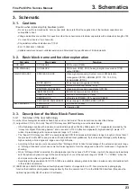
(3) In addition to sRGB, support is provided for the Adobe RGB (1998) color space, which is used as the standard color space
in the graphic design and printing fields.
• The inclusion of an additional partner chip with the UCS2 for image processing yields improved color space reproduction
and lower levels of noise.
(4) Image visibility is also improved through the use of a 2.0-inch low-temperature polysilicon TFT color LCD monitor featuring
a resolution of 235,000 pixels and 100% coverage.
(5) The use of a dedicated microchip for powering up means that media information is recorded even while the camera is
turned off, reducing the time between the camera being turned on being ready to shoot.
(6) The previous FinePix S2Pro needed 2 power supplies (2 CR123 button cells and 4 AA batteries), but the reduced power
consumption levels on the FinePix S3Pro allow it to run on a single power supply (4 AA batteries).
(7) Modifications to the base body allow improved viewfinder magnification, the adoption of D-TTL flash exposure control and
an X-sync speed of 1/180.
(8) A Firmware Update function has been included to allow for future functionality upgrades and support for special models.
3-3-2. Block function descriptions
(1) Imaging circuit (CCD BLOCK) (CAM BLOCK)
The analog video signals output from the new APS-size CCD Honeycom SRII (high-sensitivity S pixels: 6.17 million; R
pixels designed to increase dynamic range: 6.17 million) are processed using false-color correction (CDS), optimized
spacing (CDS), amplification (AGC) and signal mixing (CDS) in a single CSPIC chip (IC906; abbreviated as ACS), before
being converted (A-D) to 12-bit digital signals. The CSP-IC also incorporates the “TG/SSG” function, previously provided
as a separate IC, onto one chip. The converted digital signals are then sent to the signal processing IC (abbreviated as
UCS2; IC104; CSP).
(2) Image processor (PROCESS BLOCK) (Input data from the CCD)
The 12-bit digital image data (the section corresponding to 1H) generated by the imaging unit (CCD-CAM BLOCK) is sent
to the signal processing IC (abbreviated as UCS2; IC104), where buffer processing is performed in the IC’s internal buffer
to convert the signals to 32-bit (16-bit x 2) data (CCD-RAW data). The converted 32-bit data (CCD-RAW data) is stored in
the 16MB SDRAM (IC101 IC102 IC103 and IC106) via the I/O bus for the image signal processing IC. The image data for
each frame (4256 pixels x 2848 lines) is temporarily stored in SDRAM. Also, the 32-bit image data input to the signal
processing IC (abbreviated as UCS2; IC104) is used for additions performed by the AUTO computing unit and then sent
to the CAM BLOCK ACS (IC906) so that the optimal AE, AWB and AF values are obtained. (Recording onto the xD
Pictuer Card/Microdrive) The image data stored in the SDRAM (IC101 IC102 IC103 and IC106) is sent one line at a time
to the signal processor IC (IC104; UCS2; CSP) via the I/O bus in the signal processor IC. In the signal processor, the
data is unpacked and the following processes are called: 16 bit -> 10 bit conversion; preprocessing such as digital
clamping, gamma correction, and 10-bit -> 8-bit conversion for the R, G and B channels; YC processing to convert the 8-
bit RGB signals to Y:Cb:Cr=4:2:2, after which the Y, Cr and Cb 8-bit image data is returned to the internal buffer. In the
internal buffer, the 8-bit Y, Cr and Cb signals are sorted into a data format that facilitates DCT compression before being
recorded onto an xD Pictuer Card or Microdrive via the JPEG calculation unit and media controller. (Image playback from
the xD Pictuer Card or Microdrive) The compressed image data on the xD Pictuer Card is sent to the signal processing IC
(abbreviated as UCS2; IC104) as 8-bit image data and then sent to SDRAM (IC101 IC102 IC103 and IC106) via the
media control unit, the DMA unit and the internal buffer control unit. The image data temporarily stored in SDRAM (IC101
IC102 IC103 and IC106) is then returned to the signal processor IC (abbreviated as UCS2; IC104) and sent to the signal
processor unit via the media controller and JPEG calculation unit. The signal processor unit performs postprocessing in
which the 8-bit Y:Cr:Cb image signals are converted to 8-bit R, G and B signals. At the same time, the character display
signals are superimposed and sent to the LCD BLOCK. The imaging system adjustment data is stored in F_ROM
(IC314). The 8-bit brightness and color-difference signals processed by the signal processing IC (UCS2; IC104) are D-A
converted in the image signal processing IC encoder unit and the display character signals are superimposed, producing
analog RGB signals. Video (a composite video signal) is also included at the same time in the B component of the RGB
signal output. When the VIDEO terminal is inserted into the camera, a composite video signal is automatically output by
the detector.
(3) LCD Controller (LCD BLOCK)
The RGB analog signals output from the image signal processing IC encoder block are sent to the LCD controller IC
(IC500), where they are converted to digital RGB signals. The LCD controller IC also controls the LCD panel gradations
at the same time.
3-3-3. Description of the Power Supply Block Functions
The power supply circuit mounted on the MAIN PWB ASSY board generates a 3.3-volt (IEEE-IC IC1100, UCS2 IC401,
ACS IC906, +16V/-9.0V (CCD power supply)), 7.5-volt (LCD backlight power supply) or 12-volt (LCD panel) supply.
Содержание FinePix S3Pro
Страница 27: ...27 3 Schematics FinePix S3Pro Service Manual 3 6 Circuit Diagrams 3 6 1 CCD BLOCK ...
Страница 28: ...28 3 Schematics FinePix S3Pro Service Manual 3 6 2 DCDC BLOCK ...
Страница 29: ...29 3 Schematics FinePix S3Pro Service Manual 3 6 3 IEEE1394 BLOCK ...
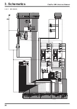
Страница 30: ...30 3 Schematics FinePix S3Pro Service Manual 3 6 4 PROCESS BLOCK ...
Страница 31: ...31 3 Schematics FinePix S3Pro Service Manual 3 6 5 CARD BLOCK 3 6 6 DCDC BLOCK CAMERA BODY ...
Страница 32: ...32 3 Schematics FinePix S3Pro Service Manual 3 6 7 PARTNER CHIP BLOCK ...
Страница 33: ...33 3 Schematics FinePix S3Pro Service Manual 3 6 8 PWON BLOCK ...
Страница 34: ...34 3 Schematics FinePix S3Pro Service Manual 3 6 9 USB2 0 BLOCK ...
Страница 35: ...35 3 Schematics FinePix S3Pro Service Manual 3 6 10 LCD BLOCK ...
Страница 36: ...36 3 Schematics FinePix S3Pro Service Manual 3 6 11 SW BLOCK ...
Страница 37: ...37 3 Schematics FinePix S3Pro Service Manual 3 7 Mounted Parts Diagrams 3 7 1 CCD PWB ASSY SIDE A SIDE B ...
Страница 38: ...38 3 Schematics FinePix S3Pro Service Manual 3 7 2 MAIN PWB ASSY SIDE A ...
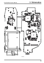
Страница 39: ...39 3 Schematics FinePix S3Pro Service Manual SIDE B ...
Страница 40: ...40 3 Schematics FinePix S3Pro Service Manual 3 7 3 SW PWB ASSY SIDE A SIDE B ...
Страница 102: ...26 30 Nishiazabu 2 chome Minato ku Tokyo 106 8620 Japan FUJI PHOTO FILM CO LTD ...

