Fuji Electric MT5F33743 Скачать руководство пользователя страница 8

MT5F33743

© Fuji Electric Co., Ltd. All rights reserved.

5-8

So, 

V

GE

is generated between gate to emitter. If 

V

GE

is excess the sum of reverse biased

voltage and 

V

GE(th)

, IGBT

2

is turned on. Once IGBT

2

is turned on, the short-circuit condition is

happened, because both IGBT

1

and IGBT

2

is under turned-on state.

Based on this principle, several measures have been devised as methods for avoiding the 

unexpected turn-on for the IGBT. These include adding a capacitance 

C

GE

component between the 

gate and the emitter, increasing -

V

GE

, and enlarging the gate resistance 

R

G

. The effect of these 

measures varies depending on the applied gate circuit. Therefore, only apply them after sufficiently 

confirming your configuration. In addition, also confirm whether there is any impact on switching loss.

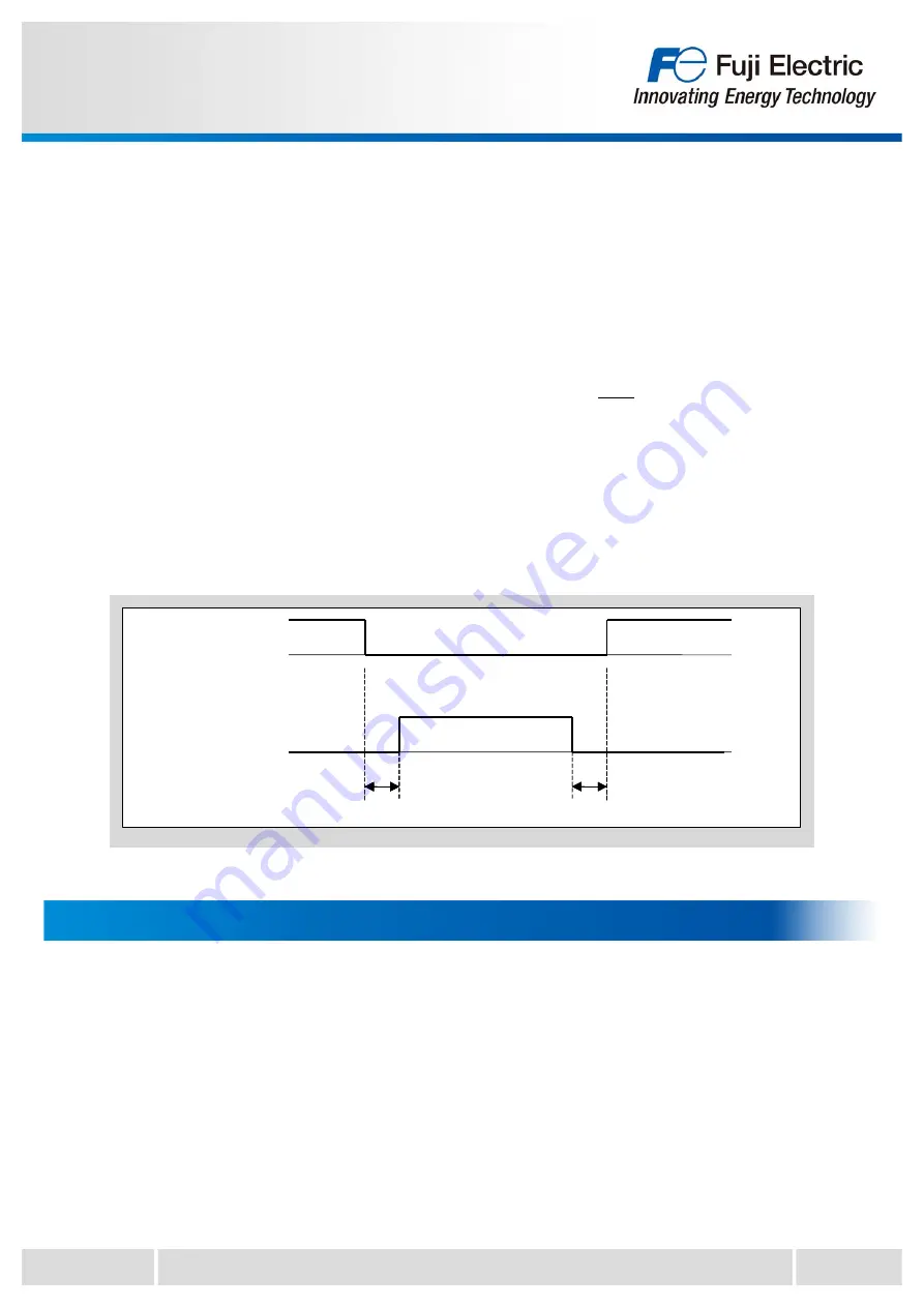
4.4 Dead time setting

For inverter circuits and the like, it is necessary to set an on-off timing delay (dead time) in order to

prevent short circuits. During the dead time, both the upper and lower arms are in the OFF state.

Basically, the dead time (Fig. 5-10) needs to be set longer than the IGBT switching time (

t

off

max.).

For example, when 

R

G

is increased, switching time also becomes longer, so it would be necessary to

lengthen dead time as well. Also, it is necessary to consider other drive conditions and the

temperature characteristics.

It is important to be careful with dead times that are too short, because in the event of a short circuit

in the upper or lower arms, the heat generated by the short circuit current may destroy the module.

Therefore, appropriate dead time should be settled by the confirmation of practical machine.

Fig. 5-10 Dead time timing chart

Dead time

Lower arm
Gate signal

Dead time

H

L

H

L

ON

ON

ON

OFF

OFF

OFF

Upper arm
Gate signal

In high capacity inverters and other equipment that needs to control large currents, it may be

necessary to connect IGBT modules in parallel. When connected in parallel, it is important that the 

circuit design allows for an equal flow of current to each of the modules. If the current is not balanced 

among the IGBTs, a higher current may build up in just one device and destroy it. The electrical 

characteristics of the module as well as the wiring design, change the balance of the current between 

parallel connected IGBTs. In order to help maintain current balance it may be necessary to match the 

V

CE(sat)

values of all devices.

Also, when the IGBT module has the cooler with the water jacket, it is necessary to adhere strictly to 

specifications such as water temperature, water flow and pressure within each water jacket.

For more detailed information on parallel connections, refer to Chapter 10 of this manual.

5. Parallel Connections

Содержание MT5F33743

Страница 1: ...imum Junction Temperature Tvjmax 5 2 2 Short Circuit Protection 5 2 3 Over Voltage Protection and Safety Operation Area 5 2 4 Operation Condition and Dead Time Setting 5 7 5 Parallel Connections 5 8 6 Electrostatic Discharge Countermeasures and Gate Protection 5 9 7 ESD Conductive Foam 5 10 ...

Страница 2: ...ned in chapter 1 this IGBT module has on chip current detecting sensor Its function and characteristics are shown in chapter 8 So please use this on chip sensor for short circuit protection function suitably On the other because this IGBT module does not have corrector voltage detecting point on each arm desaturation type of short circuit protection method shall not be used to avoid any unexpected...

Страница 3: ...s to be within RBSOA on actual system like invertor If surge voltage is excess guaranteed RBSOA surge voltage shall be suppressed by adding snubber circuit by reducing stray inductance by tuning gate resistance and so on In addition when surge voltage is reduced by gate resistance it is able to be effective operating condition to independently tune the gate resistance of turn on and turn off respe...

Страница 4: ... of SOA of FWD part 3 3 Safety operation area SOA of FWD part As same as RBSOA of IGBT SOA of FWD part is also defined SOA of diode is defined as acceptable area of maximum power Pmax which is the product of current and voltage during reverse recovery operation Therefore any system shall be designed that locus of current and voltage during reverse recovery should be within SOA An example of SOA of...

Страница 5: ...tions which happen dynamic avalanche shall not be applied because there is possibility of IGBT destruction by turn off loss increase and latch up phenomenon There are many causes of dynamic avalanche like long wiring of main circuit To prevent this dynamic avalanche IGBT module shall be used within RBSOA condition at least 5 5 Fig 5 6 An example of dynamic avalanche waveform 150 VCC 500V IC 2000A ...

Страница 6: ...le of active clamp circuits In the circuits Zenner diode and a diode connected with the anti series in the Zenner diode are added When the VCE over breakdown voltage of Zenner diode is applied IGBT will be turned off with the similar voltage as breakdown voltage of Zenner diode FWD Zenner Di Di IGBT Therefore installing the active clamp circuits can suppress the spike voltage Moreover avalanche cu...

Страница 7: ...ns under the maximum rated G E voltage VGES 20V 2 It is recommended that supply voltage fluctuations are kept to within 10 3 IGBT turn off characteristics are heavily dependent on VGE especially when the collector current is just beginning to switch off Consequently the greater the VGE the shorter the switching time and the switching loss become smaller 4 If the VGE is too small dv dt shoot throug...

Страница 8: ...cessary to consider other drive conditions and the temperature characteristics It is important to be careful with dead times that are too short because in the event of a short circuit in the upper or lower arms the heat generated by the short circuit current may destroy the module Therefore appropriate dead time should be settled by the confirmation of practical machine Fig 5 10 Dead time timing c...

Страница 9: ...le the module using the package body 3 When performing soldering work on the IGBT terminal make sure to ground the tip of the soldering iron with an adequately low resistance to ensure that static electricity is not applied to the IGBT through soldering iron or solder bath leakage Furthermore the IGBT is susceptible to breakdown if voltage is applied between the collector and emitter while the gat...

Страница 10: ... product in a piece of equipment it is requested that you only remove the conductive foam just before PCB mounting in order to prevent electrostatic discharge damage Refer to the following workflow 7 ESD Conductive Foam 5 10 4 PCB mounting and control terminal soldering 3 Conductive foam removal Fig 5 12 Conductive foam removal procedures 1 Unpacking 2 Moving process Do not remove the conductive f...

Отзывы: