Reproduction forbidden without Fibocom Wireless Inc. written authorization - All Rights Reserved.
FIBOCOM NL668-AM Hardware User Manual
Page 15 of 62
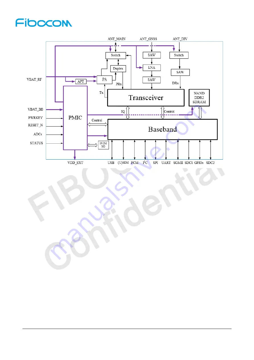
Figure 2-1 Hardware Diagram
Страница 1: ...ction forbidden without Fibocom Wireless Inc written authorization All Rights Reserved FIBOCOM NL668 AM Hardware User Manual Page 1 of 62 FIBOCOM NL668 AM Hardware User Manual Version V1 0 1 Date 2018...
Страница 2: ...ritten authorization All Rights Reserved FIBOCOM NL668 AM Hardware User Manual Page 2 of 62 Applicability type No Product model Description 1 NL668 AM 00 MCP is 4 2 and supports MAIN_ANT DIV_ANT GNSS_...
Страница 3: ...ent in any form Attention The document is subject to update from time to time owing to the product version upgrade or other reasons Unless otherwise specified the document only serves as the user guid...
Страница 4: ...2 3 Hardware Diagram 14 3 Application Interface 16 3 1 LCC Interface 16 3 1 1 Pin distribution 16 3 1 2 Pin definition 17 3 2 Power Supply 22 3 2 1 Power supply 23 3 2 2 1 8V Output 24 3 2 3 Power co...
Страница 5: ...Operating Frequency 43 4 2 RF Output Power of NL668 AM 43 4 3 RF Receiving Sensitivity of NL668 AM 44 4 4 GNSS Receiver 44 4 4 1 Basic description 44 4 5 RF PCB Design 45 4 5 1 Antenna RF connector 4...
Страница 6: ...rcuit 29 Figure 3 10 Reset Control Timing 29 Figure 3 11 SIM Card Slot Diagram SIM016 8P 220P 32 Figure 3 12 USIM SIM Interface with Detection Signal Reference Design 32 Figure 3 13 USIM SIM Interface...
Страница 7: ...el Switched AT command 34 Table 3 13 Main Serial Port Pin 35 Table 3 14 Debug Serial Port Pin 35 Table 3 15 Network Indication pins 36 Table 3 16 Network Indicator Status Description 37 Table 3 17 W_D...
Страница 8: ...Reproduction forbidden without Fibocom Wireless Inc written authorization All Rights Reserved FIBOCOM NL668 AM Hardware User Manual Page 8 of 62 Table A 0 1 Terms and Acronyms 56...
Страница 9: ...le for the consequences caused by the user s misuse Road safety first When you drive do not use the handheld devices even if it has a hand free feature Please stop and call Please turn off the mobile...
Страница 10: ...specification Radio transmission and reception FDD Part 1 Conformance specification 3GPP TS 34 122 V10 1 0 Technical Specification Group Radio Access Network Radio transmission and reception TDD 3GPP...
Страница 11: ...radiated radio frequency energy and if not installed and used in accordance with the instructions may cause harmful interference to radio communications However there is no guarantee that interference...
Страница 12: ...re guidelines for an uncontrolled environment can be satisfied The end user has to also be informed that any changes or modifications not expressly approved by the manufacturer could void the user s a...
Страница 13: ...LTE FDD Band 2 4 5 12 13 17 66 71 WCDMA Band 2 4 5 NL668 AM 01 LTE FDD Band 2 4 5 12 13 17 66 WCDMA Band 2 4 5 Data transmission LTE FDD Rel 9 150Mbps DL 50Mbps UL Cat 4 LTE Downlink MIMO 2x2 4x2 WCDM...
Страница 14: ...ID Call Transfer Call Hold Call Waiting and Multi Talk etc SMS point to point MO MT cell broadcast support Text and PDU modes MMS service Need AP to realize MMS protocol Table 2 1 Product Specificatio...
Страница 15: ...Reproduction forbidden without Fibocom Wireless Inc written authorization All Rights Reserved FIBOCOM NL668 AM Hardware User Manual Page 15 of 62 Figure 2 1 Hardware Diagram...
Страница 16: ...2 3 Application Interface 3 1 LCC Interface NL668 AM module adopts LCC packaging with a total of 144 pins 3 1 1 Pin distribution Figure 3 1 Pin Distribution Diagram TOP plan perspective diagram Note 7...
Страница 17: ...Reserved 4 W_DISABLE I VILmin 0 3V VILmax 0 6V VIHmin 1 2V VIHmax 2 0V Module flight mode control 5 NET_MODE O VOHmin 1 35V VOLmax 0 45V Module state indicate 6 NET_STATUS O VOHmin 1 35V VOLmax 0 45V...
Страница 18: ...data signal cable 16 USIM _CLK O For 1 8V USIM VOLmax 0 45V VOHmin 1 35V For3 0V USIM VOLmax 0 45V VOHmin 2 55V USIM clock signal cable 17 USIM _RST O For 1 8V USIM VOLmax 0 45V VOHmin 1 35V For 3 0V...
Страница 19: ...max 0 45V VOHmin 1 35V VILmin 0 3V VILmax 0 6V VIHmin 1 2V VIHmax 2 0V PCM clock signal 28 SDC2_DATA3 I O Reserved 29 SDC2_DATA2 I O Reserved 30 SDC2_DATA1 I O Reserved 31 SDC2_DATA0 I O Reserved 32 S...
Страница 20: ...F power input 3 3V 4 3V 58 VBAT_RF I Vmax 4 3V Vmin 3 3V Vnorm 3 8V RF power input 3 3V 4 3V 59 VBAT_BB I Vmax 4 3V Vmin 3 3V Vnorm 3 8V Baseband power input 3 3V 4 3V 60 VBAT_BB I Vmax 4 3V Vmin 3 3V...
Страница 21: ...pecification USB differential data bus 71 USB_VBUS I Vmax 5 25V Vmin 3 0V Vnorm 5 0V USB plug detection 72 GND G Ground 73 112 GND G Ground 113 NC NC 114 NC NC 115 USB_BOOT I VILmin 0 3V VILmax 0 6V V...
Страница 22: ...NC 141 NC NC 142 NC NC 143 NC NC 144 NC NC Table 3 1 Pin Definitions Note Keep the unused pins floating Pin73 Pin112 is the module thermal pad and the corresponding ground pad is reserved for PCB pack...
Страница 23: ...capacitor Battery power can be properly reduced to 100 220uF capacitor 1uF 100nF Digital signal noise Filter clock and digital signal interference 39pF 33pF 700 850 900 MHz bands Filter low band RF in...
Страница 24: ...s on or off or for external low current 80mA circuit If it is not in use keep it in floating status The logic level of VDD_EXT is defined as follows Parameter Minimum Typical Maximum Unit VDD_EXT 1 71...
Страница 25: ...750 LTE FDD Data transfer Band 5 23dBm 640 LTE FDD Data transfer Band 12 23dBm 640 LTE FDD Data transfer Band 13 23dBm 680 LTE FDD Data transfer Band 17 23dBm 680 LTE FDD Data transfer Band 66 23dBm...
Страница 26: ...cuit reference When the NL668 AM module is in power off mode the module will power on by pulling down PWRKEY for 100ms 2s It is recommended to use OC OD drive circuit to control PWRKEY pin The referen...
Страница 27: ...EY pin should not be less than 30ms 3 3 2 Module power off The module supports the following three power off modes Power off mode Power off methods Applicable scenarios Low voltage power off When VBAT...
Страница 28: ...gh level state after the power off command is executed otherwise the module will power on again after the power off complete Figure 3 7 Power off Timing Control Diagram 3 3 3 Module reset NL668 AMmodu...
Страница 29: ...All Rights Reserved FIBOCOM NL668 AM Hardware User Manual Page 29 of 62 Figure 3 8 RESET_N OC OD Drive Reference Circuit Another reset control is shown in Figure 3 9 Figure 3 9 RESET_N Button Referen...
Страница 30: ...USB_DM I O 70 USB differential data bus D USB_DP I O 69 USB differential data bus D USB_VBUS PI 71 USB_DET Table 3 9 USB Interface Definition At present USB just support USB_VBUS detect For more infor...
Страница 31: ...in is shown in the following table Pin name I O Pin Description USIM_DATA I O 15 USIM SIM DATA USIM_CLK O 16 Clock Signal USIM_RESET O 17 RESET Signal USIM_VDD O 14 USIM SIM Power USIM_PRESENCE I 13 D...
Страница 32: ...re User Manual Page 32 of 62 Figure 3 11 SIM Card Slot Diagram SIM016 8P 220P Figure 3 12 USIM SIM Interface with Detection Signal Reference Design Principles of SIM card slot with detection signal ar...
Страница 33: ...the following table AT command SIM card hot plug detection Function description AT MSMPD 1 Enabled Default SIM card hot plug detection is enabled The module detects whether the SIM card is inserted t...
Страница 34: ...ve anti interference ability The length of cable from the module to the SIM card slot shall not exceed 100mm Longer cable reduces signal quality USIM_CLK and USIM_DATA signals are ground isolated to a...
Страница 35: ...ata DBG_TXD O 12 Module Transmit data Table 3 14 Debug Serial Port Pin 3 6 2 UART port application The serial port level of NL668 AM LCC module is 1 8V If the level of the client host system is 3 3V o...
Страница 36: ...des three network indication pins Pin 5 is network status indicator by default AT commands AT LEDCFG can switch to pin 6 or pin 61 PIN Name I O PIN Num Description NET_MODE O 5 Network status indicato...
Страница 37: ...ign Diagram 3 8 Low Power Mode 3 8 1 Flight mode W_DISABLE Pin Description Pin name I O Pin Description W_DISABLE I 4 Module flight mode control Table 3 17 W_DISABLE Pin Description NL668 AM supports...
Страница 38: ...If the host does not supports USB Suspend and does not support VBUS function the module can enter sleep mode by disconnecting USB_VBUS from the external control circuit Sleep Sent AT GTLPMMODE 1 X com...
Страница 39: ...P_IN line X 0 low level active to be recall X 1 high level active to be recall 3 8 2 5 UART application DTR level control When host and NL668 module has connected through UART use the following steps...
Страница 40: ...audio interface including PCM_CLK PCM_SYNC and PCM_IN PCM_OUT 3 9 1 Support model NUM Product model Description 1 NL668 AM 00 support 2 NL668 AM 01 support Table 3 19 Support model 3 9 2 PCM interfac...
Страница 41: ...of 62 technical support 3 9 4 PCM signal description NL668 AM main chip support PCM signal adopts domestic mainstream Europe E1 standard PCM_CLK is a 2 048MHz clock in 16bit linear format encoding PC...
Страница 42: ...Parameters 3 10 ADC function NL668 AM support the 2 channels ADC interface Use AT TADC 0 to read the value on the ADC0 interface Use AT TADC 1 to read the value on the ADC1 interface The ADC range is...
Страница 43: ...MHz Bandwidth 1 RB Band 12 23 1 10MHz Bandwidth 1 RB Band 13 23 1 10MHz Bandwidth 1 RB Band 17 23 1 10MHz Bandwidth 1 RB Band 66 23 1 10MHz Bandwidth 1 RB Band 71 23 1 10MHz Bandwidth 1 RB Table 4 2 R...
Страница 44: ...97 99 10MHz Band width Band 17 98 98 10MHz Band width Band 66 97 8 98 10MHz Band width Band 71 98 99 10MHz Band width Table 4 3 RF Receiving Sensitivity Note The sensitivity in the above table is the...
Страница 45: ...s recommended that clients use the U FL R SMT 1 antenna connector and the matching RF adapter cable Antenna is a sensitive device susceptible to the external environment For example the location of th...
Страница 46: ...ground to avoid other signal cable near the antenna Recommend a complete ground level and use this complete ground level as a reference ground The ground around the antenna must be connected to the ma...
Страница 47: ...ions Gain is a collection of antenna benefits and antenna directivity Recommended antenna gain 2 5dBi 6 Interference In addition to the antenna performance other interferences on the PCB also may affe...
Страница 48: ...are User Manual Page 48 of 62 NL668 AM module main antenna requirements Input power 23dBm average power WCDMA LTE Standing wave ratio recommended 2 1 GNSS Frequency range 1559MHz 1607MHz Polarization...
Страница 49: ...ent temperature range NL668 AM module is recommended to operate at 30 75 ambient It is recommended that the application uses temperature control measures under harsh environmental conditions At the sa...
Страница 50: ...Temperature 85 3 24 hours in shutdown state Temperature shock test In shutdown state 0 5 hour at 40 and 85 environment respectively the temperature conversion time 3min for 24 cycles High temperature...
Страница 51: ...cur in the transport and secondary development so developers should consider ESD protection for the final product In addition to considering anti static treatment for packaging please refer to recomme...
Страница 52: ...l Rights Reserved FIBOCOM NL668 AM Hardware User Manual Page 52 of 62 6 Structure Specification 6 1 Product Appearance The product appearance for NL668 AM module is shown in Figure 6 1 and 6 2 Figure...
Страница 53: ...COM NL668 AM Hardware User Manual Page 53 of 62 6 2 Dimension of Structure The structural dimension of the NL668 AM module is shown in Figure 6 3 Figure 6 3 Dimension of Structure Unit mm 6 3 SMT Patc...
Страница 54: ...EGSM Extended GSM900 Band FDD Frequency Division Duplexing GMSK Gaussian Minimum Shift Keying GSM Global System for Mobile Communications HSDPA High Speed Down Link Packet Access IMEI International Mo...
Страница 55: ...Message Service TDMA Time Division Multiple Access TE Terminal Equipment TX Transmitting Direction TDD Time Division Duplexing UART Universal Asynchronous Receiver Transmitter UMTS Universal Mobile Te...
Страница 56: ...Voltage Value VImax Absolute Maximum Input Voltage Value VImin Absolute Minimum Input Voltage Value VOHmax Maximum Output High Level Voltage Value VOHmin Minimum Output High Level Voltage Value VOLmax...
Страница 57: ...n forbidden without Fibocom Wireless Inc written authorization All Rights Reserved FIBOCOM NL668 AM Hardware User Manual Page 57 of 62 Appendix B ADP MiniPCIe RF ports trace 1 NL668 AM MiniPCIe a Prim...
Страница 58: ...Reproduction forbidden without Fibocom Wireless Inc written authorization All Rights Reserved FIBOCOM NL668 AM Hardware User Manual Page 58 of 62 b Diversity Antenna...
Страница 59: ...Reproduction forbidden without Fibocom Wireless Inc written authorization All Rights Reserved FIBOCOM NL668 AM Hardware User Manual Page 59 of 62 c GNSS Antenna...
Страница 60: ...Reproduction forbidden without Fibocom Wireless Inc written authorization All Rights Reserved FIBOCOM NL668 AM Hardware User Manual Page 60 of 62 2 NL668 AM ADP a Primary Antenna...
Страница 61: ...Reproduction forbidden without Fibocom Wireless Inc written authorization All Rights Reserved FIBOCOM NL668 AM Hardware User Manual Page 61 of 62 b Diversity Antenna...
Страница 62: ...Reproduction forbidden without Fibocom Wireless Inc written authorization All Rights Reserved FIBOCOM NL668 AM Hardware User Manual Page 62 of 62 c GNSS Antenna...