
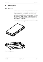


Description
A2D–JP Version 1.03 Side 13
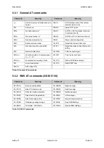
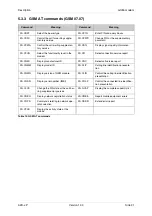
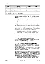
Correction Pin configuration AMP 177984-2
Pin
GSM–modem
Description
Level
1 MIC P15 Microphone 1 positive differential inp.
2 MIC N15 Microphone 1 negative differential inp.
3 SPK P2 Speaker 1 positive differential out.
4 SPK N2 Speaker 1 negative differential out.
5 DTR RS-232 Data Term. Ready CMOS 2,8 V inp.
6 CTS RS-232 Clear To Send CMOS 2,8 V out.
7 DSR RS-232 Data Set Ready CMOS 2,8 V out.
8 RTS RS-232 Ready To Send CMOS 2,8 V inp.
9 RI RS-232 Ring Indicator CMOS 2,8 V out.
10 DCD RS-232 Data Carrier Detect CMOS 2,8 V out.
11 SOFT ON Turn phone on CMOS 2,8 V inp.
12 RING PWM Ringer Interface CMOS 2,8 V out.
13 TX RS-232 Transmit Data CMOS 2,8 V out.
14 RX RS-232 Receive Data CMOS 2,8 V inp.
15 Free
16 RESET GSM Reset-Active Low SCHMITT
17 Free
18 VCCRTC RTC back-up batt. Supply inp.
19 Free
20 Free
21 Free
22 Free
23 VC5 Power supply 5 V DC
24 VC5 Power supply 5 V DC
25 VC5 Power supply 5 V DC
26 VC5 Power supply 5 V DC
27 GPIO1 General purpose in/out CMOS 2,8 V
28 VC5 Power supply 5 V DC
29 Free
30 EN Internal Power enable CMOS 2,8 V inp.
31 GROUND
32 GROUND
33 GROUND
Table 1: Pin configuration AMP 177984-2, GSM-modem
Содержание A2D-JP
Страница 1: ...Description Embedded GSM GPS Module A2D JP...


