Introduction
110121-4001A
7
1.3
Block Diagram
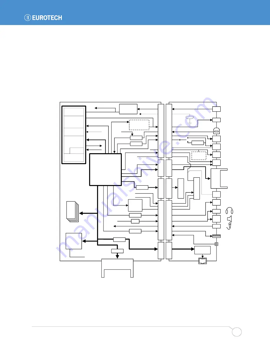
The following diagram illustrates the system organization of the Bitsy G5. Arrows indicate the
direction of control and not necessarily signal flow. Optional circuitry is drawn with dotted lines.
Connector reference designators given are for the Bitsy family products. Connector reference
designators on the Bitsy G5 are labeled differently and are shown as (Jx).
The diagram also illustrates the Bitsy G5 Personality Board. See Section 2.1.2 for additional
details about the personality board.
Ethernet
DDR SDRAM and
Flash Memory
Audio I/F
System Bus
+
Bitsy G5
J9
USB Host
Power
Supply
Personality Board
J10
PCMCIA
J1
J13
buffers
Serial 1
Serial 2
Serial 3
LCD
buffers
buffers
Freescale
i.MX31
SD/MMC
digital I/O
amp
I2C
Touch Panel
Controller
USB OTG
buffers
LCD
Serial 2
Serial 3
Serial 1
JP4-5
J18
J22
J20
J31
J16
J9
J43
J12
J44
J45
USB Function
Backlight
Touch panel
Power input
/IRDAON
J36
Wakeup
USB Host
System
Controller
Logic
buffers
buffers
J24
J2
J10
Reset button
I/O
J3
J3
J1
ADSmartIO
J37
J11
J6
J34
Power
Supplies
Touch Panel
Controller
RTC
Codec
Interfaces
BATTPOS
preamp
MIC_IN
SPKR
SPKR
MIC_IN
BATTPOS
xcvr
I2C
Board Power
SPI1.0
SPI2.0
MC13783
(J
8)
(J
9)
(J3)
xcvr
digital I/O
SPI1.1
digital I/O
SPI2.2
J7
SD/MMC
J21
J19
(J
5)
(J
4)
J8
(J
2)
LED
Backlight
I2C/SPI
SW1
I2C
I/O


