3
PCB Layout Design
3.3 Power Supply
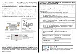
Figure 15: ESP32C3 Family Power Traces in a Fourlayer PCB Design
• Four-layer PCB design is recommended over two-layer design. Route the power traces on the fourth
(bottom) layer whenever possible. Vias are required for the power traces to go through the layers and get
connected to the pins on the top layer. There should be at least two vias if the main power traces need to
cross layers. The drill diameter on other power traces should be no smaller than the width of the power
traces.
• As shown in Figure
, an ESD protection diode is placed close to the power port (marked in red circle). A
10 µF capacitor is required before the power trace is connected to the chip, to be used in conjunction with
a 0.1 µF capacitor. Then the power traces are divided into two ways from here and form a star-shape
topology, thus reducing the coupling between different power pins. Note that all decoupling capacitors
should be placed close to the power pin, and ground vias should be added close to the ground pin of
decoupling capacitors to ensure a short return path.
• The 3.3 V power traces, highlighted in yellow, are routed as shown in Figure
. The width of the main
power traces should be at least 20 mil. The width of the power traces for pin 2 and pin 3 should be at least
15 mil. The width of other power traces is preferably 10 mil.
• As shown in Figure
, we recommend connecting the capacitor to ground in the LC filter circuit near pin 2
and pin 3 (analog power supply pins) to the third and fourth layer through a via, and maintaining a keep-out
area on other layers.
Espressif Systems
19
ESP32-C3 Family Hardware Design Guidelines V1.0


