background image

EPL-3000 /Action Laser 1300 Service Manual

Disassembly and Assembly

3.2.3 Disassembling the Engine

This section describes disassembling the engine, including the power supply board 

3.2.3.1 Optical Unit Removal

 Do not touch the optical unit except at the time of replacement.

■ 

Do not open the unit under any conditions.

■ 

Do not remove the circuit 

 the optical unit under any condition.

1.

Remove the housing. (Refer to Section 3.2.1.1.)

2.

Disconnect connector CN205 on the main board.

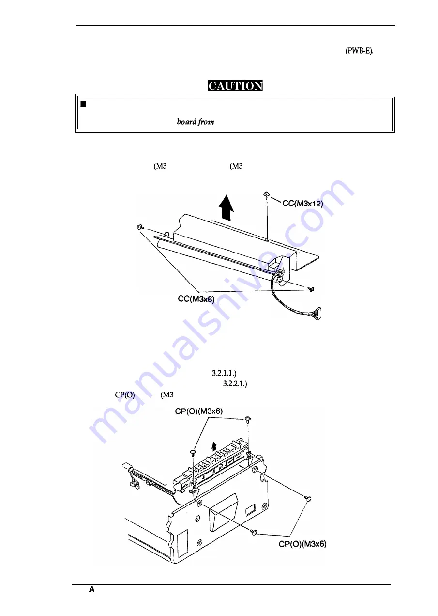
3. Remove 2 CC screws 

 x 6) and CC screw 

 x 12), and remove optical unit.

Figure 3-5. Removing the Optical Unit

3.2.3.2 Fusing Unit Removal

1. Remove the housing. (Refer to Section 

2. Remove the main board. (Refer to Section 
3. Remove 4 

 screws 

 x 6) on the fusing unit, and remove the fusing unit.

Figure 3-6. Removing the Fusing Unit

Rev. 

3-7

Содержание ActionLaser 1300

Страница 1: ...EPSON TERM NAL PR NTER EPL 3000 ActionLaser 1300 SERVICE MANUAL EPSON ...

Страница 2: ... this manual However should any errors be detected SEIKO EPSON would greatly appreciate being informed of them The above notwithstanding SEIKO EPSON can assume no responsibility for any errors in this manual or the consequence thereof Epson is registered trademark of Seiko Epson Corporation General Notice Other product names used herein are for identication purposes only and maybe trademarks of th...

Страница 3: ...for products marketed in the United States The label shown below indicates compliance with the CDRH regulations and must be attached to laser products marketed in the United States WARNING Use of controls adjustments or performance of procedures other thanthosespecified in this manual may result in hazardous radiation exposurel Internal Laser Radiation Maximum Radiation Power 3 025 X 1OA W Wave Le...

Страница 4: ...mandatory for products marketed in the United States The label shown below indicates compliance with the CDRH regulations and must be attached tolaserproducts marketed in the United States IWARNING Use of controls adjustments or performanceof procedures othe 1 thanthosesoecified in this manual mav result inhaardous radiation exDosure Internal Laser Radiation Maximum Radiation Power 3 025X 104 w Wa...

Страница 5: ...seen VARNING Osynlig laserstrNning niir denna del ar oppnad och sparren ar urkopplad Betrakta ej stri den For Norway Users ADVARSEL Dersom apparatet brukes pii annen rni e em spesifisert i denne bruksan visning kan brukeren utsettes for unsynlig laserstr ling som overskrider grensen for laser klasse 1 Dette er en halvleder laser Maksimal effeckt til laserdiode er 3 025 x 10 4 W og bolgelengde er 7...

Страница 6: ... EXPOSURE TO BEAM I VORSICHT U iJSICNTBARE LASERSTRAHLUNG WENN ABOECKUNG GE6FFNET NICNT DEM STRA L AUSSSTZEN AOYARSEL USYNLIG LASERSTRiLlffi NAR OEKSEL hJES U EKSPONERING FOR STRdLEN VARO AVATTAESSA OLET A TTllNA N KYMiTT6M LLE LASERSATEILYLLE ALA KATSO S ATEESEEN AOVARSEL USYNIJG LASERSTtiLING VED ABNING UNDG i uD 9ETTELSE FOR STf7ALlNG VARNING OSYNLIG LASERSTRiLNING NAR OENNA OEL h I WAD STF LEN...

Страница 7: ...components of the printer CHAPTER 2 OPERATING PRINCIPLES Describes the theory of printer operation CHAPTER 3 DISASSEMBLY AND ASSEMBLY Includes a step by step guide for product disassembly and assembly CHAPTER 4 ADJUSTMENT Includes a step by step guide for adjustmen CHAPTER 5 TROUBLESHOOTING Provides Epson approved techniques for adjustment CHAPTER 6 MAINTENANCE Describes preventive maintenance tec...

Страница 8: ...REVISION SHEET t T Revision laeue Date Revision Page Rev A July 22 1994 let iesue C 5 i vii ...

Страница 9: ...TABLE OF CONTENTS CHAPTER 1 CHAPTER 2 CHAPTER 3 CHAPTER 4 CHAPTER 5 CHAPTER 6 APPENDIX GENERAL DESCRIPTION OPERATING PRINCIPLES DISASSEMBLY AND ASSEMBLY ADJUSTMENT TROUBLESHOOTING MAINTENANCE Vlll ...

Страница 10: ... 3 1 2 Reverse Mode 1 11 1 3 2 Optional Interface C82305 C82306 EPL 3000 only 1 15 1 4 OPERATING INSTRUCTIONS 1 16 1 4 1 1 4 2 1 4 3 1 4 4 1 4 5 1 4 6 1 4 7 1 4 8 Control Panel 1 16 Service Mode 1 17 1 4 3 1 Hexadecimal Dump Mode 1 17 1 4 3 2 Factory Service Mode 1 17 1 4 3 3 EEPROM Format Mode 1 17 Message Display 1 18 1 4 3 1 Status and Error Messages 1 18 1 4 3 2 SewiceCall Error 1 19 Printer S...

Страница 11: ... print quality by eliminating jagged edges from images and characters Two levels 35 o less and 50 0 less for Toner Save Mode Optional EPSONScript Level 2 PostScript compatible SIMM module Optional WPS Windows Printing System SIMM module 1 MB standard RAM and up to 5 MB RAM with the addition of optional SIMM Bidirectional parallel interface High speed parallel communication rate of approximately 12...

Страница 12: ...Font SUWRS bitmap local ROM Chip language fonts Yes No Scalable Local Language Font Supports scalable local ROM Chip language fonts Yes No Thai Font ROM Chip Suppotis Thai fonts Yes No 3051020 Imaging cartridge Toner cartridge Yes Yea Serial interface card Yes No 82307W 282308X 32 KB serial interface card Yes No 28231 OW 28231 1X 32 KB parallel interface cad Yes No 282312X I LocalTalkcard Yes I No...

Страница 13: ...150 GLT EXE LG 16 to 24 lb GLG F4 HLT 60 to 90 g m2 Auto feed Standard built in Monarch Envelopes made paper tray 5 to 10 DL C5 C6 IB5 of 16 to 24 lb 60 Commercial 10 to 90 g m2 paper Manual feed 1 Any size feedable 16 to 42 lb Note 2 60 to 157 g m2 Notes 1 The weight inpounds lb is determined by how much 500 sheets cut to 17 x 22 inches would weigh l g mz 0 2659763 lb 2 Paper size range width 3 0...

Страница 14: ... Not supported Paper feed alignment and direction Center alignment for all sizes Paper ejection Face down Output tray capacity 50 sheets standard paper Printable area standard paper See Figure 1 2 Printable Areii 4 Omm I Figure 1 2 Printable Area i 4 Omm i 4 Omm 4 0 c Note The actual printable area depends on the printer mode Noise Less than 30 dB A standby Less than 47 dB A operating Ozone densit...

Страница 15: ...s or less 1 out of 1 000 sheets 30 minutes or less 5 years or 100 0000 sheets 1 2 4 Environmental Conditions for Operation Including Imaging Cartridge Temperature 10 to 35 c 50 to 95 F Humidity 15 to 8570 RH Altitude 2 500 m 8 200 feet or lower Horizontal placement The printer should be installed on a level plane Illuminance 3 000 IUX or less must not be exposed to direct sunlight Surrounding spac...

Страница 16: ...sumable Note Consumable life is based on COXItinUOtM printing mode with A4 letter paper at a 5 image ratio black white ratio The life varies depending on the printing mode continuous or intermittent and or the image ratio Environmental Conditions for Storage and Transportation Temperature Humidity Drop test Vibration Resistance to atmospheric pressure Storage term 1 2 8 Physical Specifications Dim...

Страница 17: ...ortrait s Courier 12 cpi Portrait s Courier Bold 12 cpi Portrait s Scalable fonts Dutch 801 Roman SWC s Dutch 801 Bold SWC s Dutch 801 Italic SWC s Dutch 801 Bold Italic SWC s Swiss 742 Swc s Swiss 742 Bold SWC s Swiss 742 Medium Italic SWC s Swiss 742 Bold Italic SWC s Swiss 721 Roman SWM s Swiss 721 Bold SWM s Swiss 721 Oblique SWM s Swiss 721 Bold Oblique SWM s Dutch 801 Roman SWM s Dutch 801 B...

Страница 18: ...h IBM Spanish PcMultilingual HP LaserJet 4L Mode scalable fonts 34 symbol sets Roman 8 ECM94 1 UK Legal PsMath MsPublishing Math 8 Windows IBM DN VeIntemational PcE Europe Wingdings Norwegl Swedis2 French2 8859 2 1S0 8859 9 1S0 VeMath WiE Europe PsText McText T VeUS SyrnbolT Roman Extension Italian Swedis2 UK HP Spanish Spanish Portuguese IBM US Italian ANSI ASCII German Spanish WiTurkish DeskTop ...

Страница 19: ... as parallel interface of Epson s current page printer Reverse mode 1 3 1 1 Compatibility Mode of Parallel Interface System STROBE synchronization 8 bit parallel data transfer Handshaking BUSY and ACKNLG signals Connector type P90 25027 1 Amphenol receptacle Applicable plug 57 30360 Amphenol or equivalent Transfer speed Approximately 125 XN bytes second maximum Signal timing See Figure 1 3 Signal ...

Страница 20: ...cept new data Timing with the BUSY signal is speci d through SelecType 11 BUSY OUT The BUSY signal informs the host computer of the printer state When the signal is HIGH the printer cannot accept data The PE signal indicates paper empty for the standard tray 12 PE OUT selected through SelecTyps or command or for the optional paper cassette Paper empty is indicated by HIGH 13 SLCT OUT Use in revers...

Страница 21: ...mode transmission 0000 0000 Request nibble mode 10 ACKNLG OUT PtrClk Printer data sending clock 11 BUSY OUT PtrBusy Printer sending data bits 3 and 7 during data transfer to host computer 12 PE OUT AckDataReq Printer sending data bits 2 and 6 during data transfer to host computer 13 SLCT OUT Xflag Printer sending data bits 2 and 6 during data transfer to host computer HostBusy This signal informs ...

Страница 22: ... switch diagram Compatibility Mode l o Forvvard Data Transfer STROBE ACK and BU Y JFailed SLCT IN HIGH Negotiation SLCT N LOW ERR HIGH ERR LOW No data sent Sending data I ERR LOW r AUTO FEED LOW A Reverse ERR LOW Idle AUTO I FEED HIGI H o s t Figure 1 4 Parallel Interface State Switch Diagram Q 1 12 Rev A ...

Страница 23: ...The signal is set to HIGH if the extension request value is 04h Note 3 HB DA Host Busy Data Available HB DNA Host Busy Data Not Available Figure 1 6 shows the data transfer timing chart DATA SEL IN STROBE AUTO FEED ACKNLG BUSY PE SLCT ERROR Peripheral Busy Statu Bit 3 Bit 7 X Peripheral 8usy Status Bit 2 Bit 6 N4te 1 j Bit 1 Bit 5 N e 2 Bit O Bit 4 N te 1 HB DA Negotiation HB DAor HB DNA Note 3 Fi...

Страница 24: ...mination Compatibility or HB DA Figure 1 7 Termination Timing Chart Note 1 The signal is HIGH when HB DNA The signal is LOW when HB DA Note 2 The signal is set to HIGH if the extension request value is 04h Note3 Idle LOW Figure 1 8 shows the interrupt timing chart DATA 3EL IN STROBE AUTO FEED ACKNLG BUSY PE SLCT Peripheral Busy Status Note 1 ERROR Reverse Idle Interrupt HB DA Figure 1 8 Interrupt ...

Страница 25: ...1200 1800 2400 4800 9600 or 19200 bps Error handling Overrun error Processed as missing data and replaced by Parity error Replaced by Framing error Replaced by Breaking character Ignored Handshaking When the vacant area for data in the input buffer drops to 256 bytes the printer outputs an X FF code or sets the DTR signal level to LOW indicating that the printer cannot receive more data Once the v...

Страница 26: ...or lights and buttons I Indicator lights D a t a off Slow flashing Quick flashing on Orange color H Jam Cover on Slow flashing Quick flashing Figure 1 9 Control Panel Power off Received data is stored in the printer but has not been pMted The printer is receiving or processing data There is no printable data remaining in the printer Toner low Paper jam or cover open Paper out or feed jam Warning R...

Страница 27: ...xadecimal Dump Factory Reset EEPROM Format EEPROM reset 1 4 2 1 Hexadecimal Dump Mode The hexadecimal dump mode is a useful tool for troubleshooting data control problems To enter hexadecimal dump m e turn on the printer while holding down the Toner Save Mode button until Data light comes on 1 4 2 2 Factory Reset Mode This mode resets all settings except the printer name and total printing counter...

Страница 28: ...n error statement An error follows print a status sheet The status sheet is the printed error statement Insufficient Memory Erase downloaded data or add optional memory There is not enough memory to print or download data Print Overrun If the printer cannot automsticslty recover change Engine speed faster than print the PAGE PROTECT setting by image processing with the PJL mmmand utility If the pr...

Страница 29: ...all Error This printer automatically checks the operating conditions of each component If any abnormality is detected the printer displays an error message on the control panel While the printer detects a service call error it continuously repeats the following display All lights on All lights off Error code display All lights off Table 1 10 Service Call Error Indicator Light Display II Jam T r Da...

Страница 30: ...ssing data is a maximum f 1 100 of all memory Note While EPSONScript Level 2 is used this printer sets the input buffer 1 4 5 Emulation Mode Switch Function This section describes the emulation mode switch function 1 4 5 1 Emulation Switch by SPL The two types of emulation switch functions described below are available on this printer Together they are referred to as SPL Shared Printer Language EJ...

Страница 31: ...s in eliminating jaggies in diagonal lines It is most effective when the dot map data fits the development characteristics of the printer mechanism It is therefore necessary to set appropriate values in PJL commands 1 inch 4 1 inch R 1 2 3 300 300 n Figure 1 13 Effect of RITech Note RITech is not effective for printing a screen pattern or gray scale In such cases RITech must be set to OFF The defa...

Страница 32: ...s or if you regularly use downloaded fonts you may need to install the optioml SIMM sets on this printer s controller board The printer s controller board comes with 1 0 MB of RAM installed By installing additional SWIMS you can increase the printer s memory to a total of 5 MB including the resident memory Epson supplies several types of SIMM memory options Other SIMMS can be purchased from other ...

Страница 33: ...sy removal and replacement The main components are Q C144 MAIN Board Video controller circuit and engine controller circuit board Cl ROM SIMM board Optional ROM module Q PWB E Board Power supply circuit board Cl PWB F Board High voltage supply circuit board Cl Optical Unit U Fusing Unit Cl Drive Unit Cl Imaging Cartridge Cl Housing PWB F Fusing hit PWB E Figure 1 16 Component Layout Rev A 1 23 ...

Страница 34: ... and font ROMora separate type Table 1 11 ROM and Jumper Settings Jumper Settings I ROM Locations J2 J4 IC17 IC18 IC19 IC8 1 2 1 2 4Mbit 4Mbit 8Mbit Mask EEPROM EEPROM Font ROM Code U Code L 1 2 1 2 8Mbit Mask 8Mbit Mask Code ROM Font ROM 1 2 2 3 16Mbit Mask Code Font ROM Custom ICS ASIC E05A83 lC5 ASIC E05B01 IC9 ASIC E05B04 IC13 PAL E06A01 IC22 The engine controller arcuit consists of an M37451M...

Страница 35: ...M for other software modes 1 5 3 PWB E Board The PWB E is the power supply board which consists of a switching regulator circuit It converts the AC line voltage into 12 V and 5 VDC voltages There are two types of power supply board the 120V and 220 240V type The difference between the two circuits is only in the input section Do not touch VRIE on PWB E board as it is set at the factoy and should n...

Страница 36: ...t be changed 1 D VR2F Figure 1 19 PWB F Board 1 5 5 Optical Unit The optical unit consists of the laser diode sernkonductor laser the mirror motor scanner motor which drives the polygon mirror tbr laser scannin and several mirrors and lenses The laser beam generated by the laser diode is conducted to the OPC drum surfaa by way of the polygon mirror as well as several mirrors and lenses to create a...

Страница 37: ... V type The only difference between them is the heater lamp 1 5 7 Drive Unit The drive unit consists of the main motor and a series of gears and clutches It drives the paper transport rollers OPC drum sleeve roller fusing roller and some other mechanisms Figure 1 22 Drive Unit 1 5 8 Imaging Cartridge The core mechanisms of the printing process such as charging developing and cleaning are integrate...

Страница 38: ...ol 2 9 2 1 2 2 PaperTake Up and paper Exit Sensors 2 11 2 1 2 3 FuserControl 2 12 2 1 2 4 Polygon MotorControl 2 14 2 1 2 5 LaserDiode Drive 2 15 2 1 2 6 BiasVoltages and LaserDriveTiming 2 16 2 1 2 7 Fan Motor Control 2 18 2 1 2 8 Power Supply Circuit Functions and Safety protection 2 19 2 2 VIDEO CONTROLLER OPERATION 2 20 2 2 1 C144MAlN Board Operation 2 20 2 2 1 1 Reset Circuit 2 22 2 2 1 2 Bus...

Страница 39: ...on Motor Control Circuit 2 14 Figure 2 21 Polygon Motor Driving Start Timing 2 14 Figure 2 22 Laser Diode Drive Circuti 2 15 Figure 2 23 Laser Emission Power Adjustment Timing 2 16 Figure 2 24 High Voltage Supply Block Diagram 2 16 Figure 2 25 Print Process 2 17 Figure 2 26 Print Sequence Staft 2 17 Figure 2 27 Print Sequence End 2 17 Figure 2 28 Printing Multiple Pages 2 18 Figure 2 29 Fan Motor ...

Страница 40: ...5 6 7 8 9 10 11 12 13 14 20 19 18 17 16 15 1 Paper exit tray 2 Optical unit 3 Imaging cartridge 4 Exit roller 5 Thermistor THl 6 Upper fusing roller 7 Thermal fuse TFl 8 Heater lamp Hi 9 Fusing separator 10 Paper exit sensor PC2 11 Lower fusing roller 12 cooling fan 13 Image transfer roller 14 Main motor Ml 15 Paper Take up sensor PC1 16 Transport roller 17 Paper take up roller 18 Polygon motor M2...

Страница 41: ...e Wmnd 2 1 1 Print Process This section describes the print process from paper feeding to paper exit Figure 2 2 shows a dia am of the print process n 6 3 laser Exposure L Imaging Cartridge 1 Paper Feeding 9 c I Figure 2 2 Print Process Diagram Q 2 2 Rev A ...

Страница 42: ...ler The depressing cam presses the paper lifting up plate When the paper take up solenoid SL1 is actuated the paper take up roller rotates and the depressing cam releases to feed the first sheet of paper The timing to align the leading edge of paper with the image is determined by the paper take up sensor PC1 Both of the sensors are comprised of a photo interrupter and an actuator When the paper t...

Страница 43: ...prea a thin ewm coat of toner over the flexible sleeve As toner passes between the doctor blade and the flexible sleeve it becomes negatively charged though friction These are used to rotate the flexible skeve This transports toner to the surface of the PC drum and ccmtrols developing l he latent image is formed by laser beams on the surface of the PC drum and development is carried out by the fle...

Страница 44: ... Laser Exposure Laser exposure is the process Imaging Cartridge A Drum Charge Bias B Developing Bias C Doctor Blade Bias D Drum Ground Figure 2 5 Drum Charge of creating an invisible static electric image on the PC drum with laser beams emitted from the optical unit The mirror motor scanner motor rotates the four sided mirror counterclockwise to produce a laser light scan One side of the mirror pr...

Страница 45: ...image is transferred onto paper any remaining toner on the PC drum is scraped off by the cleaning blade and collected in the used toner bottle 2 1 1 7 Image Transfer Image transfer is the process of transferring to the paper the toner image created on the PC drum during development his printer uses the roller image transfer method instead of corona image transfer as the image transfer process In r...

Страница 46: ...if it becomes dirty After the power is turned on the heater lamp lights until the temperature of the upper fusing roller reaches 168 C 334 F After warm up the mechanical control board controls the on off operation of the heater lamp based on Controller Board the TH1 ignals from the thermistor Thermal Fuse TH1 signals Heater Lamp 1 b Thermistor d Upper Fusing Roller Lower Fusing I 5T Roller 1 Photo...

Страница 47: ...AIN I um 2 10 shows the engine controller connections 1 Polygon Scanner motor PWB D LD drive board Paper Exit Sensor PC2 Main Controller Board C144 MAIN Hgh vottage Suppiy Board PWB F Doctor Wade image Transfer CH2 Developing Bias Drum Charge CH1 GND2 1Paper Take Up Sensor PCl I 4Paper Take Up Solenoid SL1 I Power SW I Power AC Power Input supply Board PWB E Fan Motor I Figure 2 10 Engine Controll...

Страница 48: ...tioml feeding drive Figures 2 11 through 2 16 show the positions of the gears and rollers Figure 2 11 Gear Position Image Transfer Roller 4 Revolution 1497 r p m process Speed 3 23 51 mmIs 2 z leeve 11 10 9 8 3 2 Roller Figure 2 12 P C Drive Figure 2 13 Developing Drive rExit Roller Transport Roller Paper Take Up Roller i 17 r Upper Fusing Roller Revolution 28 09 r p m 16 Process Speed 23 50 mm s ...

Страница 49: ... roller 8 57 18 50 9 29 30 19 15 Exit roller 10 26 27 20 16 image transfer roller Figure 2 16 shows the main motor drive circuit The main motor Ml is a four phase stepping motor This motor is controlled by the CPU IC201 on the main controller board C144 IN The power supply board PWB E has a stepping motor driver IC This IC drives the main motor Ml with a constant current Main controller board Powe...

Страница 50: ...n detection of condition 1 below the paper is ejected and all elements are then deactivated if only the condition 1 below is detected elements other than the heater lamp Hi are deactivated since there is no paper in the fusing unit The paper take up sensor PC1 is not turned on within the specified time after the paper take up roller starts to rotate The paper take up sensor PC1 is on when the powe...

Страница 51: ...d by THl exceeds 200 W 392 F the voltage applied to 1 202 pin 42 becomes higher than the reference voltage at IC202 pin 41 Then the outout from comparator goes from HIGH to LOW When this occurs the output from the NAND ircuit goes frdm LOW ti HIGH thus turning off H1 Heater Lamp ON OFF Signal JQ l r Thermistor TH1 analog voltage i IJ _kEl C144 MAIN Board TH1 Signal 7 DC5V R207 R206 IC201 H L L H C...

Страница 52: ... occur the printer detects a fuser error 1 2 3 4 The thermistor temperature is checked 12 seconds after warm up starts and continues for the next 18 seconds If during that time the temperature of the thermistor falls to within 20 C 68 F of the ambient room temperature a fuser error is detected If the thermistor temperature does not reach 168 C 334 F within 80 seconds after the warm up starts a fus...

Страница 53: ...H SEL POLCLK POLYGNM GND 2 12 1 2 3 4 5 B Figure 2 20 Polygon Motor Control Circuit The rotation of the polygon motor M2 is detected within 5 seconds after starting the motor If the SSCAN signal is not detected properly during this period the printer assumes that the polygon motor M2 is malfunctioning and stops the motor c Polygon Motor On sec I I M2 ON SSCAN I I Illlllllimlllll lllllllllllll 1111...

Страница 54: ...otioff signal When it is L the laser is allowed to emit and when it is H the laser is stopped emitting LDVR1 This signal adjusts the laser drive current so that the laser emission becomes the regulated value rough adjustment LDVR2 This signal adjusts the laser drive current so that the laser emission becomes the regulated value fine adjustment This signal indicates whether the laser drive current ...

Страница 55: ...upply board PWB F If the printer detects a case open condition the interlock switch is set to off which cuts the 12 VDC and in turn cuts the bias voltages These bias voltages are controlled by the main board C144 MAIN The CHXJN signal is the image transfer roller bias voltage control While this sigmd is LOW the image transfer roller is charged to 3 5K VDC by the high voltage supply circuit While t...

Страница 56: ...Development Transfer Figure 2 25 Print Process Print Main Motor On v sec t Laser Exposure Development Image Transfer Paper Take up Solenoid A Paper Take up Sensor On Figure 2 26 Print Sequence Start Figure 2 27 shows the end of the print sequence The printer stops the main motor Ml from rotating when the paper exit sensor turns off after 4 72 seconds Print v sec Drum Charge Laser Exposure Image Pa...

Страница 57: ...s For 2 seconds after power on Between 20 seconds after the start of printing and 20 seconds after the end of printing For 20 seconds after all elements are stopped for detecting trouble with the exception of a except paper jam If the fan motor s current detecting potential remains at 150 mV or less for 2 seconds the fan motor is assumed to be malfunctioning Note Current detecting potential means ...

Страница 58: ...ies 5 VDC and 12 VDC The 12 VDC is used as the bias voltage supply main motor Ml drive scanner mirror motor M2 drive fan motor M3 drive and solenoid drive For safety protection the 12VDC line is cut when the interlock switch case open switch is off AC IN Power Supply Board PWB E Inter Lock Sw 12 VDC 5 VDC SG FG Figure 2 30 Power Supply Circuit Block Diagram Rev A 2 19 ...

Страница 59: ...144 MAIN Board Block Diagram Table 2 3 lists the functions of the C144 MAIN board elements Table 2 3 Functions of C144 MAIN Board Elements Element Location Function 66000 CPU IC6 The CPU which operates at 16 67 MHz manages the video controller circuit ODeration This ASIC contains the folbwing functions Interrupt control Address decoding ASIC E05A63 IC5 Cbck control DRAM management refresh control ...

Страница 60: ...s transmitted to the engine controller board If such an error occurs increase the V RAM using printer settings The CPU transmits image data stored in the V RAM to a temporary buffer in the SRAM which is located in an address space different from the CPU The temporary buffer has a capacity equivalent to several lines This is controlled by theASIC which synchronizes and transmits the te mporarybuffe...

Страница 61: ...vices comected to the RESET line This circuit uses an M51953B IC to monitor the supply voltage and reset the CPU if a voltage level less than 4 25 V is detected The reset time is approximately 840 ms 5V L 7 f Vcc OUT b RESET M51953BFP lCl c Figure 2 33 Reset Circuit 2 2 1 2 Bus Control Circuit The 68 111 CPU outputs the R W read write AS address strobe and Fco Fcl and Fc2 processor status signals ...

Страница 62: ... an automatic vector interrupt This initializes the interrupt process ASIC E05A83 has a controller for the automatic vector interrupt 2 2 1 4 DRAM Management The video controller circuit uses DRAMs for the system RAM and for the V RAM The DRAMs including optional SIMMS are managed by ASIC E05A83 and E05B01 ASIC E05A83 handles the main management The E05A83 outputs RAS CAS WE and OE signals The DRA...

Страница 63: ...he system RAM to the SRAM using ASIC EQ5A83 The ASIC converts the image data in the SRAM from parallel to serial synchronizes it and then transmits it to the engine controller circuit In other words the SRAM is a temporary buffer used to transmit the image data to the engine controller arcuit This serial image data is the VIDEO signal of the video interface The signal line of the internal video in...

Страница 64: ...nit Removal 3 7 3 2 3 3 Heater Lamp Removal 3 8 3 2 3 4 Power Supply Unit PWB E Removal 3 8 3 2 3 5 High VoKageSupply Board PWB F Removal 3 9 List of Figures Figure3 1 Removing the l lousing 3 4 Figure3 2 Removing the13earFrame 3 5 Figure3 3 Pulling theShieldcase 3 6 Figure 3 4 Removing the Main Board 3 6 Figure 3 5 Removing the Optical Unit 3 7 Figure3 6 Removingthe Fusing Unit 3 7 Figure 3 7 Rem...

Страница 65: ...e imaging cartridge If the imaging cartridge is removedfiom the printer do not place it in the direct sunlight H Do not disassemble the optical unit w Never turn power on if the optical unit is not installed To prevent damage to ICsfrom static electricity do not touch the ICS on the circuit board or the terminals of peripheral electrical components with your hands w Use only the recommended tools ...

Страница 66: ...bbreviations Table 3 2 Abbreviations Used for Screws Abbreviation Part Name CC screw Cross recessed Cup head CP 0 screw I Cross recessed Pan haad with Outside toothed lock washer CPB screw Cross recessed Pan head B tight Table 3 3 Screw Types and Abbreviations Head Body washer Top Side assembled 1 Gross recessed 1 pan 1 Normal 1 Qutside toothed head lock washer m O 2 Jlql 2 B tight J J l o n 3 2 R...

Страница 67: ...sheet Is the status sheet print performed normally I Data print Does data print in all modes Is the gap between the top edge of the paper and Adjustment Print position the horizontal line in the feature print exactly 14 6 mm 0 57 inch ROM version Is it the latest version T Is toner and dust removed from the paper path Cleaning Is the paper take up roller cleaned Is the roller in the fusing unit cl...

Страница 68: ...ly in reverse 3 2 1 Housing Removal This section describes how to remove the cases and the rear frame 3 2 1 1 Caae Removal 1 2 3 4 5 6 7 8 Open the top cover Remove the imaging cartridge Cover the imaging cartridge to protect it from the light or place it in a dark area Remove the CC screw M3 x 8 and panel cover Remove the paper tray Remove 2 CC screws M3 x 8 and the front cover Remove interfa cov...

Страница 69: ...he imaging cartridge Cover the imaging cartridge to protect it from the light or place it in a dark area 2 Remove the housing Refer to Section 3 2 l l 3 Remove 7 CP 0 screws M3 x 6 and CC screw M3 x 6 and lift the rear frame 4 Disconnect comector CNl on thepowersupply board PWB E Figure 3 2 Removing the Rear Frame Rev A 3 5 ...

Страница 70: ...Section 3 2 1 1 2 Dismnnect all 5 connectors on the main board 3 Remove the 8 CC screws M3 x 6 that secure the shield case on the right side of the printer 4 Remove the shield case with main board c Figure 3 3 Removing the Shield Caae 5 Remove the3 CP screws M3 x 6 that secure the interface shield plate on the shield case 6 Remove the 3 CP screws M3 x 6 and main board with interface shield plate 7...

Страница 71: ... not remove the circuit boardfiom the optical unit under any condition 1 Remove the housing Refer to Section 3 2 1 1 2 Disconnect connector CN205 on the main board 3 Remove 2 CC screws M3 x 6 and CC screw M3 x 12 and remove optical unit CC M3X6 Figure 3 5 Removing the Optical Unit 3 2 3 2 Fusing Unit Removal 1 Remove the housing Refer to Section 3 2 l l 2 Remove the main board Refer to Section 3 2...

Страница 72: ...Section 3 23 2 2 Remove the CC screw M3 x 8 for the heater lamp support plate and remove it 3 Remove the heater lamp CC M3X8 Figure 3 7 Removing the Heater Lamp 3 2 3 4 Power Supply Unit PWB E Removal 1 Remove the housing Refer to Section 3 2 l l 2 Remove the rear frame Refer to Section 3 2 l 2 3 Disconnect connectors cN2 CN3 and CN40nthe power supplybcwd PWB E 4 Remove 2 CC screws M3 x 6 and 3 CP...

Страница 73: ...F Removal 1 Remove the housing Refer to Section 3 2 l l 2 Remove the rear frame Refer to Section 3 2 1 2 3 Disconnect connectors CN1 and CN2 on thehighvoltage supply board PWB F 4 Remove 3 CPB screws M3 x 8 and remove the high voltage supply board Figure 3 9 Removing the High Voltage Supply Board Rev A 3 9 ...

Страница 74: ...Chapter 4 Adjustment Table of Contents 4 1 ADJUSTMENT 4 1 4 1 1 Print Position Adjustment 4 1 List of Figures Figure 4 1 Print Position Adjustment 4 1 Figure 4 2 Position of VR201 4 1 ...

Страница 75: ...d the printing of a Status Sheet is the correct value as follows STATUS SHEET page 14 6 mm 0 57 inch If not adjust the print position as described in the next few steps 14 6 mm 0 57 inch Leading Edge Figure 4 1 Print Position Adjustment 3 Turn the printer power off 4 Remove therightcase Refer to section 3 2 l l 5 While holding the control panel adjust the image synchronizing adjustment volume VR20...

Страница 76: ...e LEDs Do Not On 5 2 Table 5 5 The LCD Displays Paper Jam or Cover Open 5 3 Table 5 6 The LCD Displays Paper Empty or Feed Jam 5 4 Table 5 7 The LCD Displays Fusing Unit Error 5 5 Table 5 8 The LCD Displays Laser Light Error 5 5 Table 5 9 The LCD Displays Scanner Motor Error 5 5 Table 5 10 The LCD Displays Fan Motor 5 5 Table 5 11 The LCD Displays EEPROM Format Error 5 5 Table 5 12 The LCD Display...

Страница 77: ...section describes the self diagnostic function in which the controller automatically checks the operating conditions of each component If any abnormality is detected the printer displays an e or message on the LED It enables repeat displays as follows All LED ON ALL LED OFF Error code display ALL LED OFF Table 5 1 lists the error code messages Table 5 1 Error Code LED Display Jam Toner Data Cover ...

Страница 78: ...pfays laser light error 5 8 Scanner motor error displayed The LCD displays scanner motor error 5 9 Fan motor error displayed I The LCD displays fan motor error 5 1o I EPROM format error displayed The LCD displays EEPROM format emor 5 11 RAM error displayed The LCD displays RAM error 5 12 ROM error disdavecf The LCD disdavs ROM error 5 13 Other error Other error 5 14 I Tabie 5 3 The Printer Does No...

Страница 79: ...there The PWB E board maybe an outputof 12 VDC 4 between pin 4 and pin 3 No Replace the dead for CN3 on PWB E PWB E board board Sensor may be bad 5 Does the LEDs display cover N open error at power on Skip to step 8 Paper take up sensor may 6 Replace the paper be dead take up sensor Paper exit sensor may be 7 Replace the exit dead sensor The imaging cartridge may s Is the imaging cartridge No Inst...

Страница 80: ... With power on does the multimeter detect any current Disconnect connector CN2 on the PWB E board and check the coil resistance between pin 1 and pin 5 pin 2 and pin 5 pin 3 and pin 5 and pin 4 and pin 5 4 points total on the disconnected cable side of the Replace the main connector using a multimeter motor Pin 1 Pin 5 Pin 2 Pin 5 Pin 3 Pin 5 Pin 4 Pin 5 Are the resistances of all four rhe main mo...

Страница 81: ...ep Checkpoint Finding Solution The optical unit may be bad 1 Replace the optical unit The C144 MAIN board may 2 Replace the C144 be bad MAIN board Table 5 9 The LCD Displays Scanner Motor Error Cause Step Checkpoint Finding Solution The optical unit may be 1 Replace the optical dead unit The C144 MAIN board 2 Replace the C144 may be dead MAIN board Table 5 10 LCD Displays Fan Motor Cause Step Chec...

Страница 82: ...eplace the C144 be bad MAIN board Table 5 13 LCD Displays ROM Emor Cause Step Checkpoint Finding Solution The ROMs on the C144 1 Is the operation OK after Replace the ROMs on MAIN board may be bad you replace the ROM the C144 MAIN board The c144 MAIN board may 2 Replace the C144 be bad MAIN board Table 5 14 The LCD Displays SERVICE REQ C111O I Cause Step Checkpoint Finding Solution I The c144 MAIN...

Страница 83: ...to see if the Image transfer surface of image Replace the image Image transfer roller transfer roller is transfer roller problem damaged PWB F board Replace the PWB F board Check to see if PPer Replace paper Paper problem Paper is moist Defective optical Optical unit Replace the optical unit unit Improper print density setting Adjust the print density Foggy background Replace the imaging Imaging P...

Страница 84: ...Replace the PWB F board Imaging Replace the imaging Poor development cartridge cartridge PWB F board Replace the PWB F board improper print density setting Adjust the print density Defective optical Optical unit Replace the optical unit unit O hite black lines Shake the imaging and bands Imaging cartridge E Improper charging dtige Replace the imaging cartridge 4BC E PWB F board Replace the PWB F t...

Страница 85: ...he paper oner smudges on ack side of pages b Image transfer Check the surface of image transfer Clean the image A 4j roller transfer roller roller a G D Smears on paper path ABCDE ABCDE Fusing roller Clean the fusing roller Other paper Check the paper paths path Clean the paper path rint offset n Check if there is ABCDE any dust or Improper fusing Fusing roller damage on the Clean or replace ABC D...

Страница 86: ...sumable Replacement Service Maintenance 6 1 6 1 6 1 6 3 6 1 2 1 Periodic Service Maintenance Listof Figures Figure 6 l Shakingthelmaging Cartridge Figure 6 2 Figure 6 3 Figure 6 4 Table 6 1 Removing the Clear Seal Imaging Cartridge Settings Imaging Cartridge Settings i 2 List of Tables Maintenance 6 1 6 2 6 2 6 2 6 3 ...

Страница 87: ...efore cleaning it Wipe the cover and external parts of the printer with a damp cloth that has been soaked in a neutral cleaning solution Internal Cleaning Be sure the printer has been disconnected from the power supply and that the fusing unit has cooled down Clean printer inside using a soft cloth 6 1 1 2 Consumable Replacement This printer uses consumable imaging cartridge SO51O2O The life of th...

Страница 88: ...ng cartridge into the printer by placing the pins on each side of the cartridge into the grooves inside the printer Slide it gently into the opening until it stops 7 Push down on the front of the cartridge until it locks in place Figure 6 3 Imaging Cartridge Settings 1 8 Close the upper unit Figure 6 4 Imagin Ca idge Settings 9 If the printer displays toner low message hold down the Continue butto...

Страница 89: ...vice rnaintemnce because they are subject to functional deterioration as the total number of printed pages increase resulting in bad print quality Table 6 1 Periodic Service Maintenance Unit Service Interval Optical unit Approx 50 000 pages Fusing Unit Approx 50 000 pages I The service interval listed above is only a reference value You do not need to perform service maintenance exactly at this ti...

Страница 90: ...A 12 PWB E 120V Board Circuit Diagram A 13 Figure A 7 PWB E 220 240V Board Circuit Diagram A 14 Figure A 8 PWB F 120V Board Circuit Diagram A 15 Figure A 9 PWB F 220 240V Board Circuit Diagram A 16 Figure A 10 C144 MAIN Board Component Layout Front Side A 17 Figure A 1 1 C144 MAIN Board Component Layout Rear Side A 18 List of Tables Table A 1 Board Connector Summary A 3 Table A 2 CN2 Pin Assignmen...

Страница 91: ...s A 1 and A 2 illustrate the intercomection of the primary components Table A 1 gives the size and a description of each connector Main Board C144 MAIN Board CN 1 Parallel l F L 3 RAM SIMM N6 CN2 CN5 I Option l F Card ROM SIMM Figure A 1 Cable Conne A n for the Video Controller Rev A A 1 ...

Страница 92: ...Appendix EPL OOO ActianLasar 13 M Srvice Manual I 3Z mr a Figure A 2 Cable Connections for the Engine Section c H 7 M A A 2 Rev A ...

Страница 93: ...tor for optical unit 13 pins Table A 9 CN207 Not used 2 pins Power Supply Board PWB E Board CN1 Connector for fan motor 2 pins Table A 1 O CN2 Connector for main motor 5 pins Table A 1 1 CN3 Connector for main board C144 MAIN board 10 pin Table A 5 CN4 Connector for interlock switch 2 pins Table A 1 2 High Voltage Supply Board PWB F Board CN1 Connector for paper take up solenoid 2 pins Table A 1 3...

Страница 94: ... I o o 1 0 o 0 o 0 0 0 0 0 0 0 o 0 0 0 0 0 0 0 0 Vo Description Ground Data bus bit O DTACK for CPU Data bus bit 1 Not connected Data bus bit 2 Not conneded Data bus bit 3 Clock 5 VDc Read strobe Address bit O Address bit 1 Address bit 2 Address bit 3 Address bit 4 Address bit 5 Address bit 6 Address bit 10 Data bus bit 4 Not connected Data bus bit 5 Address bit 22 Data bus bit 6 Address bit 21 Da...

Страница 95: ...d Data bus bit 14 Not connected Data bus bit 15 Not connected Not USed Not USed Not USed Not USed Address bus bit 15 Ground Table A 4 CN6 Pin Assignments Signal Name Vss DQO DQ16 DQ1 DQ17 DQ2 DQ18 DQ3 DQ19 Vcc NC MAO MAI MA2 MA3 MA4 MA5 MA6 MAl O DQ4 DQ20 DQ5 DQ21 DQ6 I o 1 0 1 0 1 0 1 0 1 0 1 0 1 0 1 0 o 0 0 0 0 0 0 0 1 0 1 0 1 0 1 0 1 0 Description Ground Data bus bit O Data bus bit 16 Data bus ...

Страница 96: ...43 CAS1 o CAS 1 44 RASO o RAS O 45 RAS1 o RAS 1 46 NC Not connected 47 o Write enable 48 NC Not connected 49 DQ8 1 0 Data bus bit 8 50 DQ24 1 0 Data bus bit 24 51 DQ9 1 0 Data bus bit 9 52 DQ25 1 0 Data bus bit 25 53 DQ1O I o Data bus bit 10 54 DQ26 1 0 Data bus bit 26 55 DQ11 1 0 Data bus bit 11 56 DQ27 1 0 Data bus bit 27 57 DQ12 1 0 Data bus bit 12 58 DQ28 1 0 Data bus bit 28 59 Vtx 5 VDC 60 DQ...

Страница 97: ...C 2 GND1 Ground 3 PC2 I Paper exit sensor signal Table A 8 CN204 Pin Assignments Pin No Signal Name I o 1 GND1 2 Pcl I 3 DC5V 4 DC12V 5 GND2 6 CH1 ON o 7 CH2 ON o 8 DB CNT o 9 SL1 ON o Pin No 1 2 3 4 5 6 7 8 9 10 11 12 13 Description Ground Paper take up 5 VDC 12 VDC Ground Drum charge on Image transfer on Developing bias control Paper take up solenoid on Table A 9 CN205 Pin Assignments Signal Nam...

Страница 98: ...n CN2 Pin Assignments Pin No Signal Nama I o Description I 1 q A o Ml phase A 2 o Ml phase B 3 pfi o Ml pkse 4 o Ml phase 5 DC12V 12 VDC Tabie A 12 CN4 Pin Assignments Pin No Signal Name Uo Description 1 DC12V 12 VDC 2 Dcl 911 12 VW L I I A 1 3 High Voitage Suppiy Board PWB F Board Pin Assignments Tabie A 13 CN1 Pin Assignments Pin No Signal Name Ifo Description 1 DC12V 12 VDC I 2 I SL1 ON o I Pap...

Страница 99: ...EPL 3000 ActionLaser 1300 Service Manual Appendix w t t j 1 vy K JzL l LklQA 1111 1 1 L w 1 1 Iii T u ma 4 1 T Figure A 6 PWB E 120V Board Circuit Diagram Rev A A 13 ...

Страница 100: ...Appendix EPL OO ActionLaaar 1 Servide Manual ni 1 I L L O j In 0 I t 1 L RI t J H I n J iii5 a L a I I 0 Figure A 7 PWB E 220 240V Board Circuit Diagram 1 c 1 Rev A ...

Страница 101: ...EPL 3000 ActionLaser 1300 Service Manual Appendix Figure A 4 C144 MAIN Board Circuit Diagram 2 2 Rev A A n ...

Страница 102: ...Appendix EPL 30m ActbnLaaer 1 Serwca Manual n w w z 1 0 z u u l a u m U I In c m Figure A 5 C144 SUB Board Circuit Diagram A 1 2 Rev A ...

Страница 103: ...16 CIRCUIT R115 I R116 T output 1 D104 Type A C203 0205 R216 ihl 1 i R211 R215 R217 C20 4 c 0207 212 0208 CONTROL 206 R 213 R218 CIRCUIT R 214 C206 I 7A 7 JI R315 R312 R313 R31L R317 R318 1 BL CONTROL R316 C302 z D2 CIRCUIT II o C304 C303 7 output GND ANODE Iul PSI J Figure A 8 PWB F 120V Board Circuit Diagram output output Rev A A 15 ...

Страница 104: ...te B Analog i n ut o Ov 7 Type 1ST R I D104 Tv e A 16 T output R217 Coutput D208 R218 L R315 R312 R313 R31L R317 R318 BL CONTROL CIRCUIT GND ANODE I PSI 1 1 C302 Z D2 T l B 3 D303 f R323 output output c s c t1 Figure A 9 PWB F 22 V240V Board Circuit Diagram G A 16 Rev A ...

Страница 105: ...EPL 3000 ActionLaser 1300 Service Manual Appendix A 3 CIRCUIT BOARD COMPONENT LAYOUT o N z l I i I IC8 Figure A 10 C144 MAIN Board Component Layout Front Rev A A 17 ...

Страница 106: ...Appendix EPL OtW ActionL8sef 13CW Service Manual R14 17 5 R16 am HIYIS 2014838 00 11 R 0 OhO13 00 0 O c Figure A Il C144 MAIN Board Component Layout Rear A 18 Rev A ...

Отзывы: