Hardware
Design notes for the RF pad version
XBee Wi-Fi RF Module User Guide
31
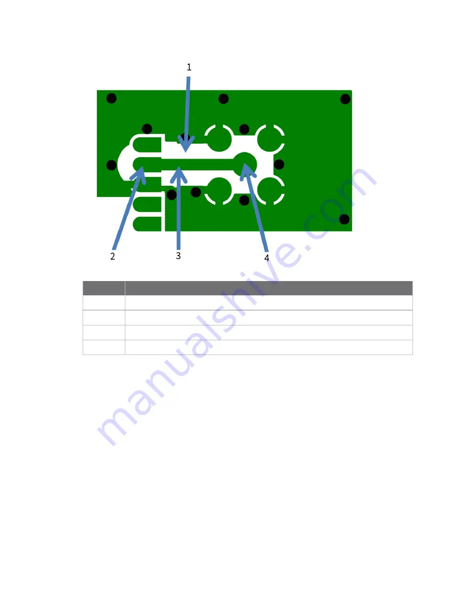
Number
Description
1
Maintain a distance of at least 2 d between microstrip and ground fill
2
Device pin 36
3
50 Ω microstrip trace
4
RF connection of RPSMA jack
This figure shows PCB layer 1 of the RF pad layout.


