PCIe-FRM11 User’s Manual (Rev 1.4)
-
7
- http://www.daqsystem.com
You can control these functions using API provided by DAQ system.
PCI Target
/ Master
PCI BUS
Local Bus
Address
Data(Mem,I/O)
Reserved
(0x00
–
0x5F)
Reserved
(0x70
–
0xAF)
UART
(0x60)
Camera Link(LVDS)
(0xC0)
Interrupt controller
DIO
(0xD0)
Ext. Address, Data, Control
Local BUS
Interrupt
Controller
(0xb0)
INT sources in Chip
IO Decoder
MEM Decoder
To each IO
Module
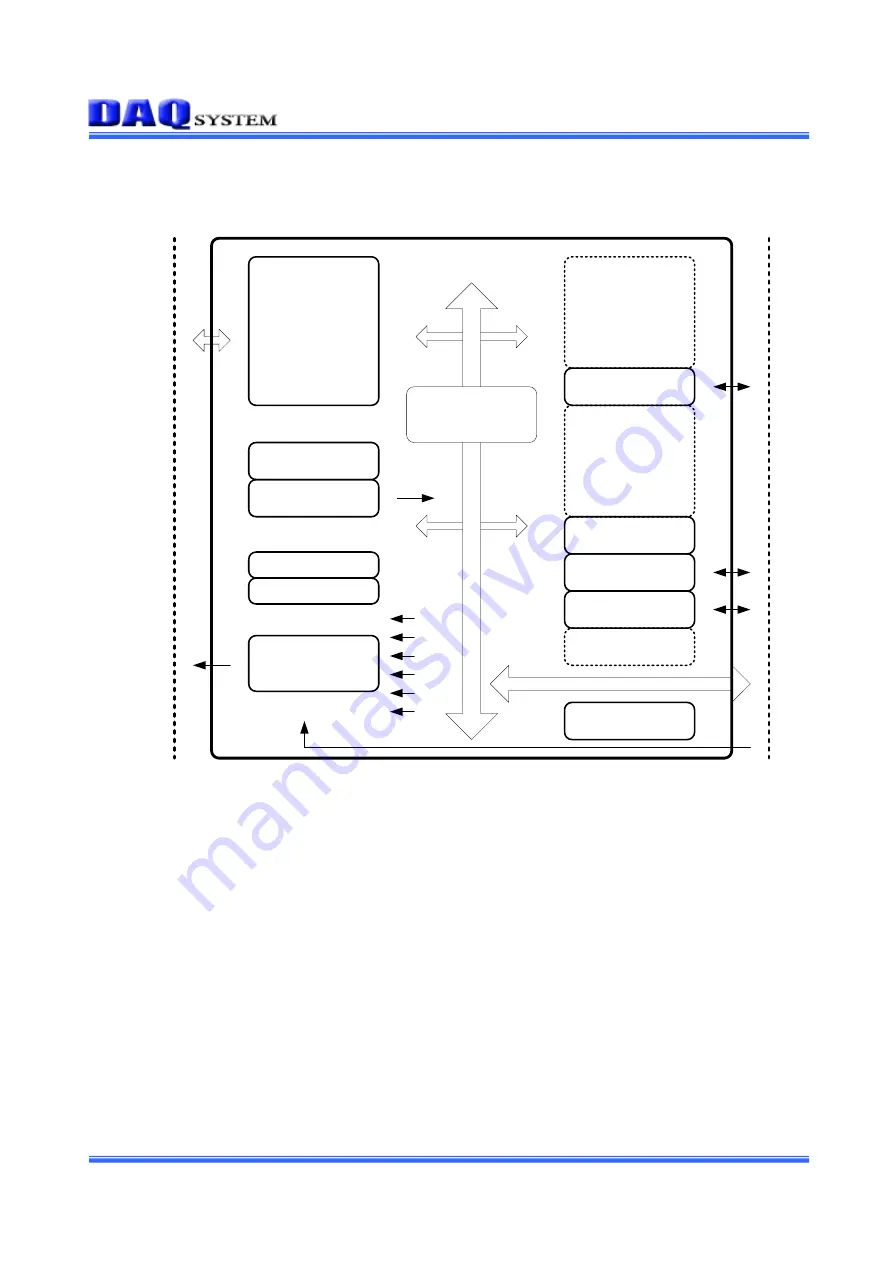
PCIe-FRM11 INTERNAL BLOCK - FPGA
DPRAM
From Ext.
CLOCK syn.
MEM Decoder
BUS Mux
Reserved
(0xE0
–
0xFF)
[Figure 2-2. FPGA Block Diagram]
The core logic program of the FPGA is loaded by JTAG. It saves a program at the FPGA Program
Logic and loads when power-up.
PCIe-FRM11 supports Camera Link Base Configuration. Base Configuration consists of 4 LVDS
signal lines that serialize 28 bit parallel signals including 24 data bits and 4 enable signals Frame Valid,
Line Valid, Data Valid, and a spare, and one LVDS signal line to synchronize with camera ,
Asynchronous serial communication for communicating with the camera, including four CC (Camera
Control) signals. All 11 LVDS signal lines, including two LVDS lines, are transmitted over the MDR
cable.
The transmitted signal is deserialized through the Channel Link chip in the PCIe-FRM11 into four
image LVDS serial signals into a 28-bit parallel video signal and control signals (Frame Valid, Line
Содержание PCIe-FRM11
Страница 22: ...PCIe FRM11 User s Manual Rev 1 4 22 http www daqsystem com click Next as in the figure...
Страница 24: ...PCIe FRM11 User s Manual Rev 1 4 24 http www daqsystem com Figure 4 2 System Properties window Hardware Tab...
Страница 37: ...PCIe FRM11 User s Manual Rev 1 4 37 http www daqsystem com A 2 Physical Dimension P1 J1 120 8 68...


