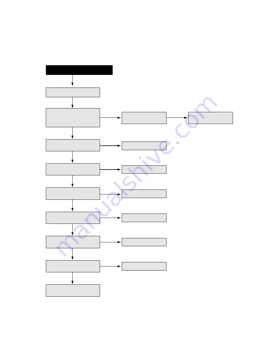
background image

84

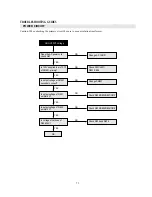
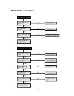
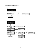
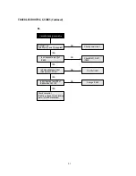
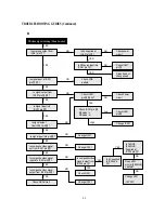
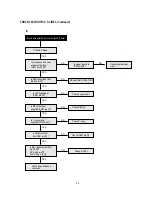
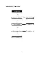
TROUBLESHOOTING GUIDES (Continued)
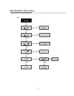
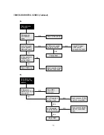
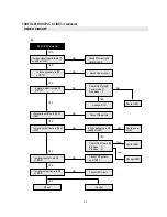
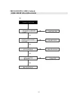
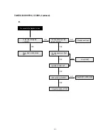
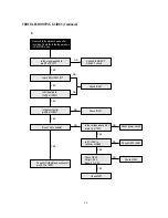
YES

C.

Is Iuminance and color
signal output from
IC301 pin 

1

,

?

YES

NO

Is REC color and FM luminance
signal input into ICA01 pin 

&

,

?

Is +5V supplide at
ICA01 pin 

?

Is REC(H) signal
supplied ICA01 pin 

?

Check EP mode

YES

YES

YES

YES

YES

YES

YES

Is signal input into
IC301 pin 

?

NO

Check input selector
circuit

NO

NO

NO

NO

NO

NO

Change ICA01

Check IC601 pin 

8

Check C. sync

Check REC(H)

Check power circuit

Check RA01, RA02, CA11

Is C. sync: signal
supplied ICA01 pin 

Is SW pulse input
into ICA01 pin 

Is REC signal output from
pin 

?

Check video head and
connector

Record video signal NG (2 head model)

Содержание DV- K584N-SJ

Страница 1: ...Technical Service Guide MONO TECHNICAL MANUAL DV K584N SJ K584N JJ K584N SG K484N SJ K484N JJ K484N SG K384N SJ K284N SJ K584NY SJ M K584NZ SJ M K584NZ SG M DV K504N SJ K504NY SG X K304N SJ...

Страница 2: ...sec SLP 11 13mm sec Maximum Recording Time T 60 3 hours SLP mode T120 6 hours SLP mode Fast Forward Rewind Time 3 minutes T 120 tape Tuning System Auto Program Cable Compatible Frequency Synthesis FS...

Страница 3: ...AC Millivolt Meter Sensitivity 1 0mVAC 400VAC Dual Trace Triggered Oscilloscope with Lo Cap X10 and Direct Probes Response DC 20MHz Sensitivity 5mV div Max Sweep Rate 0 1 sec div Frequency Counter 7...

Страница 4: ...3 EXTENSION CABLE CONNECTION A C HEAD PCB TO CAPSTAN MOTOR CABLE2 TO DRUM MOTOR CABLE1 CABLE3 P201 P502 P601 P501 MAIN PCB L C MOTOR PCB...

Страница 5: ...t board with the DECK assembly connected To imitate the function of the sensors insert the SVC Mode Diode D707 on the MAIN circuit board as shown below STOP EJECT CH DN POWER CH UP D707 REC REW FWD PL...

Страница 6: ...pply heat to both electrodes When the solder on both electrodes is melted remove leadless component with a twist ing motion LEADLESS CHIP COMPONENT REMOVAL INSTRUCTION Note a Leadless component must n...

Страница 7: ...r removing solder chips from IC s pins use a solder remover or a wiry solder absorber 2 Heat the IC s tips evenly by moving the chip IC replacing tool around them and detach the IC s leads with a tool...

Страница 8: ...tion 1 Chip Resistor Identification Standard Chip Resistor Code 2 Chip Capacitor Identification There is no identification of chip capacitor REMARK Leadless CHIP Components are identified on schematic...

Страница 9: ...assette CTL Control CUR Current CV Composite Video D D Drum Digital Diode Drain DC Direct Current DD DC DC Convert DEEM or DEEMPH Deemphasis DEMOD Demodulator DET Dectector DEV Deviation DFG Drum Freq...

Страница 10: ...robe SVC Service SW or S W Switch or Switching Pulse SYNC Synchronization SYSCON System Control T TJ Test Jump TP Test Pin TR Transistor TRANS Transformer TRK Tracking TU Tuner U UHF Ultra High Freque...

Страница 11: ...ION FRONT VIEW NOTE Model K584N SJ K584N JJ K584N JG K484N SJ K484N JJ K584N JG K384N SJ K284N SJ K584NY SJ M K584NZ SJ M K584NZ SG M NOTE Model K504N SJ K304N SJ REC REW PLAY FF POWER STOP EJECT CH R...

Страница 12: ...completed Press rewind button at playback mode to reverse the scan ning on the programmed program material visibly When the picture reaches to the point where you are looking for press the PLAY butto...

Страница 13: ...m when attached RF OUT Connector Passes signal to TV the cable supplied Audio Input Connector Receives audio signal for recording sound from a view cam era external sound equipment or another VCR Audi...

Страница 14: ...Removal Fig 3 1 Remove the top cover and the front panel 2 Remove two 2 screws 3 Lift out the bottom cover in the direction of the arrow F L Door Removal Fig 4 1 Open the F L door 90 degrees 2 Remove...

Страница 15: ...the Deck Assembly in the direction of the arrow Main PCB Assembly Removal Fig 7 1 Remove the top cover the front panel the bottom cover the preamp assembly and the deck assembly 2 Release two 2 tabs A...

Страница 16: ...al Ass y 10 T Main Brake Ass y 11 T Sub Brake Ass y 12 Relay Lever 13 Capstan Motor 14 Pinch Lever Total Ass y 15 L C Bracket Total Ass y 16 Cam Gear 17 AC Head Total Ass y 18 T Slant Pole Ass y 19 Dr...

Страница 17: ...late 23 Reel Belt 24 Reel Gear Total Ass y 25 Record Safety Lever 26 Loading Lever L 27 Loading Lever R 28 Drum Total Ass y 29 Loading Rack 0 Q q W w E Fig 10 Tape Transport Mechanism Identification B...

Страница 18: ...Prism Link R 4 Release Lever 5 Loading Lever R 6 CST Holder Ass y 7 Loading Shaft 8 Loading Lever L 9 Door Opener 10 Safety Lever 11 Safety Lever R 1 Fig 11 Front Loading Mechanism Identification Top...

Страница 19: ...tte holder assembly Fig 13 4 Remove one 1 screw holding the prism link R and remove the prism link R from the F L bracket R Fig 14 5 Remove one 1 screw holding the prism link L Fig 15 6 Release hook B...

Страница 20: ...pe path adjustment procedures in the Mechanical Adjustment section of this service publication Reel belt Loading Rack Loading Gers and S T Slant Pole Removal Fig 19 20 1 Turn the Deck Mechanism updide...

Страница 21: ...L C bracket assembly from the deck mechanism Fig 22 NOTE When reassembling refer to Fig 23 for alignment instructions Replacement of Pinch Lever Total Assembly Removal Fig 22 1 Remove one 1 washer 2 U...

Страница 22: ...assembly from the main base 4 Unhook the T sub brake spring from the main base and discon nect the T sub brake lever assembly from the main base Tension Band Assembly Removal Fig 26 27 1 Remove the t...

Страница 23: ...remove one polywasher 2 Release the tab B of the main base and part the reel gear total ass y from the main base 3 Push the connect plate to the left direction and separate it from the main base NOTE...

Страница 24: ...when reassembling parts in this mechanism be sure to confirm the following instructions to con firm the following 1 Make sure that the datum hole of the cam gear A is aligned with the hole B in the m...

Страница 25: ...onfirm that the two 2 triangular marks are aligned with each other in the EJECT mode Fig 3 4 Make sure that the boss A of the Pinch Lever Total Ass y is positioned at the point B of the cam gear in EJ...

Страница 26: ...ading Gear R Ass y in EJECT mode Fig 5 6 Make sure that the teeth of the Loading Rack are aligned with the those of the Loading Gear R so that the hole C of the Loading Rack aligns with the circular m...

Страница 27: ...The measured result must meet the specification 35 55 gr 4 If the result is not within the specification get rid of cassette torque meter from the mainbase and adjust the tension spring If the measure...

Страница 28: ...n 4 If the mechanism is in the desired mode remove the Power Tension Pole Position Adjustment 1 Make the mode PLAY without a cassette loaded Refer to Operating the VCR Without a Cassette Tape 2 Confir...

Страница 29: ...er the normal circumstances will not require adjustment However if noise appears in the playback picture then either the tape damage occured or the tape path has been changed and readjust ment of the...

Страница 30: ...IC DIAGRAM OF TAPE TRANSPORTING SYSTEM 29 2 1 3 TENSION POLE T GUIDE ROLLER S GUIDE POST A C HEAD FE HEAD T GUIDE POST S GUIDE ROLLER CAPSTAN SHAFT S SLANT POLE PINCH ROLLER DRUM VERTICAL POST T SLANT...

Страница 31: ...r edge of the tape and the edge of the AC Head is 0 25 mm 3 If the measure gap exceeds 0 25 mm turn the AC Head Height Screw CCW If not turn it CW Repeat this process until the measuring meets the spe...

Страница 32: ...pin on the Path Adj Fixture 4 Connect the channel 2 scope probe to the envelope test pin on the Path Adj Fixture Externally trigger the scope using the SW pulse test pin on the Path Adj Fixture 5 Adju...

Страница 33: ...on the Path Adj Fixture 5 Adjust the VR Control on the Path Adj Fixture so that the envelope signal of the test tape is maximum 6 Operate VCR in the Review mode for approximately 15 sec onds and then...

Страница 34: ...adjustment procedure reconfirm Fine Adjustment of Envelopes at Drum Entrance Exit Parts 12 X Axis Adjustment Fig 19 Test Points CTL Pulse Test Pin Path Adj Fixture Envelope Test Pin Path Adj Fixture O...

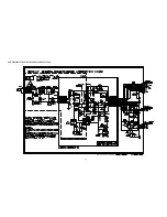
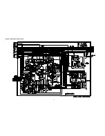
Страница 35: ...34 AC001 K584NZ SJ M K584NZ SG M only...

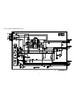
Страница 36: ...35...

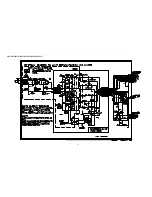
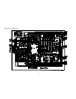
Страница 37: ...36...

Страница 38: ...37...

Страница 39: ...38...

Страница 40: ...CHING PULSE 19 Q Vsync P56 RTP6 OUTPUT Q Vsync OUTPUT PULSE 20 A SWP P55 RTP5 OUTPUT AUDIO SWITCHING PULSE 21 RECORD CTL P54 RTP4 TB2in OUTPUT PULSE 22 CAP FG P53 RTP3 CPFGin INPUT CAPSTAN FG INPUT HI...

Страница 41: ...LOCK OUTPUT SERIAL 80 PLL STB P100 CTSO RTS 0 OUTPUT PLL STROBE HIGH 81 Vcc Vcc INPUT Vcc 82 A D Reference Vref INPUT REFERENCE Vcc 83 TV LINE P101 PWM 2 OUTPUT TV LINE INPUT MODE SWITCHING H L 84 REC...

Страница 42: ...s of modes This amplified signal becomes a waveform in point A and then output to CTL waveshaping through C508 Rec CTL signal is recorded to CTL terminal by pin 21 during Rec mode CTL wavesheping circ...

Страница 43: ...r circuit Reel sensor is directly inserted on main PCB and the transmission type is applied as below Capstan motor speed in high speed rewind mode is controlled by calculating the remain time of a tap...

Страница 44: ...4 FL display Bias Circuit 1G 2G 3G 4G 5G 6G 7G 8G P1 a a a a a a a P2 b b b b b b b P3 c c c c c c c P4 d d d d d d d P5 e e e e e e e P6 f f f f f f f P7 g g g g g g g P8 P9 h P10 j P11 P12 D717 3 9...

Страница 45: ...H 3CH OPEN 4CH GND RF 3 MB MODULATOR B 5V MODULATOR 4 CONTROL MODULATOR OUTPUT SW ON VCR MODE OFF TV MODE 5 VIDEO INPUT MODULATOR VIDEO INPUT 6 BP TUNER PLL IC B 5V 7 BT TUNER B 32V 8 PLL CLOCK PLL CL...

Страница 46: ...xer IC IF Amp SAW Filter Video Detector SIF Filter FM Detector AFT VHF OSC UHF Mixer UHF RF Amp UHF OSC PLL IC AGC TV 4 5 8 AUDIO IN CH SW VIDEO IN CLOCK DATA ENABLE AUDIO OUT AFT OUT VIDEO OUT ANT IN...

Страница 47: ...ins 2 3 and 4 Operates at H level 2 0 to Vcc 6 F SAP Mode control switch connects to GND At L GND SAP discrimination automatic selection mode 7 FORCED Selection of monural and stereo operations 8 MS 0...

Страница 48: ...nput to audio part In case of mono model video signal output of TMI is input to Pin 12 of SW IC where as video signal from input jack is input to Pin 1 of SW IC and Audio signal output of TMI is input...

Страница 49: ...NRSW circuit Mode discrimination Stereo discrimination is executed through the detection of the pilot signal amplitude SAP discrimination is executed by means of the 5fH carrier and noise detection a...

Страница 50: ...PF SBU OUT ST IN C5 L R RV4 SAP FM DET SAP BPF SAP LPF SAP OUT SAP IN NR SW dbx TV BLOCK MODE CONTROL R2 R3 C2 INJ LOCK SAP DET SAP LED DRIVE MODE CONTROL L R DSB DET Fig 2 Block Diagram Refer to Fig...

Страница 51: ...and Y signal are separated by COMB FILTER and the color signal only passes through 3 58 BPF ACC AMP automatically controls burst level After Burst Emphasis boosts burst signal 6dB 3 58MHz carrier is i...

Страница 52: ...The stabilized signal is input to main converter and mixed with the 4 21MHz signal come from sub converter Its output is 4 21MHz 629KHz The mixed signal is input to 3 58 BPF in order to pass 3 58MHz...

Страница 53: ...LOR KILLER 2HD 7 Buf Buf AGC AMP SP EP HEAD LUMINANCE IC A01 REC COLOR PROCESS 6 8 31 3 18 11 17 10 18 IC151 LINE JACK INPUT SELECT TMI Buf Buf AGC AMP SP EP HEAD CHROMA IC A01 2 3 34 AGC AMP 6M LPF C...

Страница 54: ...CD QV QH INSERT Y C MIX PICTURE CONTROL DOUBLE NOISE CANCELLER NONLINEAR DEEMPHASIS VIDEO AMP OSD LINE JACK TMI 10 IC302 IC S01 10 HEAD 14 11 5 16 18 28 9 SP EP IC A01 IC 301 1 3MHz LPF ACC AMP CCD CO...

Страница 55: ...input output command switch 13 NTSC PAL NTSC PAL switch input output command switch 14 3 58 4 43 3 58 4 43 switch input output command switch 15 AST Reset input 16 CV OUT Video signal output 17 VDD2...

Страница 56: ...udio IC Features i 1 chip type including PB amp Line Amp REC amp ALC circuit EQ switch Auto REC bias circuit ii It is equipped with EQ switch which operates in SP LP EP modes respectively iii ALC leve...

Страница 57: ...n circuit R202 R203 and is input to REC Amp and output to Line out too ALC ALC point is fixed to 6dBv output inside of circuit and ALC time can be adjusted by R201 and C202 PB mode The signal read by...

Страница 58: ...by comparator Standard Voltage is 320 mVrms If it is bigger or smaller than standard Voltage the compara tor Changes the voltage of Pin 3 So that the BIAS signal which input to pin 1 is always 320 mV...

Страница 59: ...high band frequency inside of IC itself without Peaking Coil using reactance of R P Head This is a different to prior Audio circuit So to adjust frequency characteristics in this circuit we are using...

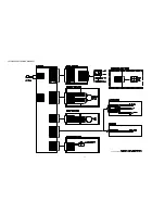
Страница 60: ...59 ELECTRICAL ADJUSTMENTS Fig 1 Circuit Board Location...

Страница 61: ...60 ELECTRICAL ADJUSTMENTS 2HEAD 4HEAD MODEL A V JACK PT01 DECK ASSAMBLY POWER SUPPLY PG SHIFTER R595 FRONT Fig 2 Main board test point control location guide Component R...

Страница 62: ...ver tical jitter 1 Load the instrument with an alignment tape and play back the color bar signal or monoscope signal 2 Connect channel 1 scope probe 1V div 50 sec div to PT01 PIN Trigger the scope on...

Страница 63: ...6 520mVp p 200mV 10 sec cm REC IC301 27 510mVp p 200mV 10 sec cm REC IC301 29 550mVp p 200mV 10 sec cm REC IC301 29 550mVp p 200mV 10 sec cm PLAY IC301 30 520mVp p 200mV 10 sec cm REC IC301 30 540mVp...

Страница 64: ...WAVEFORMS 2 IC301 37 5 2Vp p 1V 5msec cm PICTURE SEARCH 3 IC301 39 2 4Vp p 1V 10 sec cm REC 3 IC301 39 2 4Vp p 1V 10 sec cm PLAY 4 IC301 44 5Vp p 2V 10msec cm REC PLAY 5 IC301 49 600mVp p 200mV 0 5 s...

Страница 65: ...20mV 0 2msec cm REC 7 IC301 59 1 5Vp p 0 5V 0 2msec cm REC 8 IC301 60 0 3Vp p 50mV 0 2msec cm REC 9 IC301 64 2Vp p 0 5V 0 2msec cm REC 0 IC301 8 85mVp p 20mV 0 5msec cm PLAY T201 5 60Vp p 30V 20 sec c...

Страница 66: ...5Vp p 2V 5 sec cm REC PLAY IC601 4 5Vp p 2V 5 sec cm REC PLAY Q IC601 18 5Vp p 2V 5msec cm REC PLAY q IC601 23 5Vp p 2V 10msec cm REC PLAY W IC601 24 5Vp p 2V 0 5msec cm REC PLAY w IC601 22 5Vp p 2V 0...

Страница 67: ...4 8 3 0 0 0 0 0 0 2 5 4 0 0 0 0 1 5 0 1 5 5 1 1 1 1 2 2 1 1 1 1 1 1 1 1 6 0 3 0 3 0 3 0 3 0 3 0 3 0 3 7 0 2 5 0 0 0 0 0 0 8 1 7 1 0 4 2 3 0 4 2 3 0 4 2 9 0 0 0 0 0 0 0 10 2 3 3 5 2 2 2 2 2 2 2 2 2 2 1...

Страница 68: ...1 9 2 0 35 3 0 3 0 3 0 3 0 3 0 3 0 3 0 36 5 0 5 0 5 0 5 0 5 0 5 0 5 0 37 0 5 0 5 0 5 0 5 0 5 0 5 0 5 38 0 0 0 0 0 0 0 39 1 8 1 8 1 8 1 8 1 8 1 8 1 8 40 4 0 4 0 4 0 4 0 4 0 4 0 4 0 41 2 0 2 2 2 2 2 2...

Страница 69: ...5 0 C 0 0 0 0 0 0 0 B 0 7 21 0 7 21 0 7 21 0 7 Q202 E 0 17 5 0 17 5 0 17 5 0 C 0 0 0 0 0 0 0 B 0 7 21 0 7 21 0 7 21 0 7 Q203 E 5 5 0 7 3 0 5 5 5 5 5 5 5 5 5 5 C 5 8 5 8 5 8 5 8 5 8 5 8 5 8 B 5 8 0 7...

Страница 70: ...0 0 8 5 0 5 0 5 0 5 0 5 0 5 0 5 0 9 0 1 0 1 0 1 0 1 0 1 0 1 0 1 10 0 1 0 1 0 1 0 1 0 1 0 1 0 1 11 0 0 0 0 0 0 0 12 0 0 0 0 0 0 0 13 0 0 0 0 0 0 0 14 0 0 0 0 0 0 0 15 5 0 5 0 5 0 5 0 5 0 5 0 5 0 MODE...

Страница 71: ...12 10 0 9 0 12 11 0 9 0 12 12 5 0 5 0 13 0 0 14 5 0 5 0 15 0 5 0 16 9 0 9 0 12 MODE PIN NO EE REC EE REC TUNER LINE Q152 E 2 5 2 5 C 0 0 B 1 7 1 7 Q153 E 0 0 C 0 0 B 5 0 0 Q154 E 0 0 C 0 2 0 2 B 5 0...

Страница 72: ...EW REV FWD REC PLAY F FWD SEARCH PAUSE PAUSE 44 0 0 5 2 0 5 2 0 5 2 45 0 0 0 0 5 2 0 5 2 46 0 0 0 0 5 2 0 5 2 47 5 2 5 2 5 2 5 2 5 2 5 2 5 2 48 5 2 5 2 5 2 5 2 5 2 5 2 5 2 49 0 0 0 0 0 0 0 50 0 0 0 0...

Страница 73: ...0 MODE IC DRIVE PIN No STOP REC PLAY REW REV FWD REC PLAY F FWD SEARCH PAUSE PAUSE 6 0 0 0 0 0 0 0 7 12 4 12 4 12 4 12 4 12 4 12 4 12 4 8 12 4 12 4 12 4 12 4 12 4 12 4 12 4 9 0 9 0 9 0 9 0 9 0 9 0 9 0...

Страница 74: ...ed to pin of SM801 primary Is output voltage of SM801 secondary correct Is output voltage of Q801 emitter 9V Is voltage of cathode of D806 32V OK Change AC CORD Change SM801 Check R804 D802 D807 C810...

Страница 75: ...1 75 Are 20 and 16 5V supplied to pin and of G701 1 35 Is 5V at pin of IC601 37 Check X602 Check IC601 Check the L604 L606 D803 Check power circuit Check the power circuit and D717 Check IC604 Is 5V a...

Страница 76: ...0V at pin and of IC601 26 81 Do pin and of IC601 oscillate 42 Is 5V applied to pin of IC601 37 Check IC601 Check C813 Check X601 R636 R635 C605 and C606 NO YES YES YES YES NO NO NO B C 43 Check the I...

Страница 77: ...ES NO 83 14 18 Check the video output signal pin of IC151 NO YES NO YES 14 80 YES E Is 5V supplied to pin of IC601 76 YES NO Is GND applied to pin of IC601 75 YES Is 5V applied to pin of IC601 37 YES...

Страница 78: ...Q of IC601 YES NO NO Check IC601 NO Noise appears although change cassette tape CTL HEAD height is normal and there is not dust YES Check CTL in circuit R515 C510 C511 CTL AMP circuit R512 R513 R514...

Страница 79: ...eck pattern Is Enve waveform supplied to at pin of PT01 YES NO Check VIDEO circuit Check connector Head Amp and Clean heads Is Reel pulse applied to pin and of IC601 YES NO YES NO Check REEL sensor pa...

Страница 80: ...nd DRUM Motor J YES YES Check power circuit NO Is 12V supplied to P501 pin YES NO Is the voltage of pin P501 3 2V YES Check R521 R522 NO Is the voltage of P501 pin 2 5V YES Check IC601 and C FG NO Is...

Страница 81: ...NO Are Rin and Fin applied to of IC602 NO Is CAM SW DATA C601 pin W w E and e Correct YES YES YES Check IC601 Check IC602 and loading motor Check connector P601 and CAM SW in DECK Meckanism YES NO Ch...

Страница 82: ...YES NO M Is 6V applied to pin of IC602 NO Change IC602 Pin R of IC601 Is 5V applied to pin of IC602 when CST IN YES NO Is 6 2V applied to pin of IC602 when CST IN YES NO Check connector P601 pin and...

Страница 83: ...PCB pattern Is signal input into pin o of IC301 YES NO Is signal output from pin I of IC301 YES NO Check IC601 YES Check Power circuit Change IC151 Is signal Input into pin 8 of ICS01 YES NO Is signa...

Страница 84: ...eck IC601 pin p Change IC301 Change Q301 Change IC301 Is composite video signal output from IC302 pin Is 5V supplied to IC302 pin Is CLOCK 3 58MHz Supplied at IC303 pin Does X301 crystal 3 58MHz oscil...

Страница 85: ...supplied ICA01 pin Check EP mode YES YES YES YES YES YES YES Is signal input into IC301 pin o NO Check input selector circuit NO NO NO NO NO NO Change ICA01 Check IC601 pin 8 Check C sync Check REC H...

Страница 86: ...in I YES Check OSD circuit NO NO YES NO Low High NO YES NO YES NO NO NO NO NO NO YES YES Is 5V supplied at ICA01 pin 5 Check PCB pattern Check IC301 pin y 5V Check IC301 pin q EE mode L PB mode H Chec...

Страница 87: ...REC H signal supplied ICA01 pin Is C sync signal supplied ICA01 pin Is SW pulse input into ICA01 pin Is REC signal output from pin 8 7 SP mode pin 7 SLP mode pin 8 Check video head and connector Check...

Страница 88: ...Continued YES F Is composit video signal output from IC301 pin I YES NO Is 5V supplied at ICS01 pin e 7 YES YES NO Check IC601 NO Check Power circuit Change ICS01 Check serial data ICS01 pin OSD Chara...

Страница 89: ...INPUT JACK Is 0V of Pin d F f Check SYSCON circuit Is there output at pin H of IC301 Change IC301 Check OUTPUT JACK Is 5V applied to pin y J of IC301 Is signal input pin G of IC301 in Line mode YES Y...

Страница 90: ...ut at pin H of IC301 Check R221 R222 R203 C221 Is 5V applied to pin y J of IC301 Is 5V applied to pin F of IC301 Is 0V collector of Q201 Check Pin of P201 NO NO Check power circuit NO Check IC601 NO C...

Страница 91: ...01 YES NO Check power circuit NO YES NO Check Q203 YES YES Is there output at pin d of IC201 Does T201 oscillate YES YES Check A C HEAD and connector pin of P201 Check Q203 Collect 5 8V Base 0 7 3 0V...

Страница 92: ...91 INTERCONNECT WIRING DIAGRAM K584N K484N K384N K284N...

Страница 93: ...92 POWER SUPPLY SCHEMATIC DIAGRAM FREE VOLTAGE K584NY SJ M K584NZ SJ M K584NZ SG M...

Страница 94: ...93 POWER SUPPLY SCHEMATIC DIAGRAM 120V ONLY K584N SJ K584N JJ K584N SG K484N SJ K484N JJ K484N SG K384N SJ K284N SJ K504N SJ K504NY SG X K304N SJ...

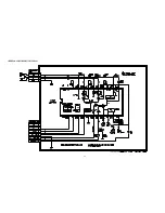
Страница 95: ...94 2HD HEAD AMP SCHEMATIC DIAGRAM K384N K284N K304N...

Страница 96: ...95 4HD HEAD AMP SCHEMATIC DIAGRAM K584N K484N K504N...

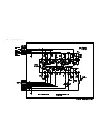
Страница 97: ...96 VIDEO AUDIO SCHEMATIC DIAGRAM K584N K484N K384N K284N K504N K304N...

Страница 98: ...97 PIF INPUT SELECTOR SCHEMATIC DIAGRAM 9V USE K584NY SJ M K584NZ SJ M K584NZ SG M...

Страница 99: ...98 PIF INPUT SELECTOR SCHEMATIC DIAGRAM 12V USE K584N SJ K584N JJ K584N SG K484N SJ K484N JJ K484N SG K384 SJ K284N SJ K504N SJ K504NY SG X K304N SJ...

Страница 100: ...99 TIMER SYSCON SCHEMATIC DIAGRAM K584N K484N K384N K284N K504N K304N...

Страница 101: ...100 POWER SUPPLY BLOCK DIAGRAM FREE VOLTAGE K584NY SJ M K584NZ SJ M K584NZ SG M...

Страница 102: ...101 POWER SUPPLY BLOCK DIAGRAM 120V ONLY K584N SJ K584N JJ K584N SG K484N SJ K484N JJ K484N SG K384N SJ K284N SJ K504N SJ K504NY SG X K304N SJ...

Страница 103: ...102 2HD HEAD AMP BLOCK DIAGRAM K384N K284N K304N...

Страница 104: ...103 4HD HEAD AMP BLOCK DIAGRAM K584N K484N K504N...

Страница 105: ...104 VIDEO AUDIO BLOCK DIAGRAM K584N K484N K384N K284N K504N K304N...

Страница 106: ...105 PIF INPUT SELECTOR BLOCK DIAGRAM K584N K484N K384N K284N K504N K304N...

Страница 107: ...106 SYSCON SERVO BLOCK DIAGRAM K584N K484N K384N K284N K504N K304N SEG A SEG L SEG A SEG L SEG C SEG F G1 G8 G1 G8...

Страница 108: ...7P5043000 1 EX300 SCP150 EX300 4 MANUAL OWNERS 97P9560000 1 ALL MODEL 5 CABLE RF 97P880RN15 1 NTSC 1 5M 6 COVER ACCESSORY 97P0424100 1 LD PE TO 1 7 REMOCON HADSET AS 97P1R2BZ00 1 VR F2BR 97P1R2BR04 1...

Страница 109: ...108 MAIN PCB 2HEAD 4HEAD...

Страница 110: ...GND CAPSTAN MOTOR TO MAIN P501 1 2 3 4 5 6 D MTR VCC D SPD CTL DRUM PG DRUM PG DRUM GND DRUM FG DRUM MOTOR TO MAIN P502 DRUM MOTOR PCB 1 2 3 4 5 6 CTL HEAD CTL HEAD A PB HEAD A REC HEAD AUDIO GND A E...

Страница 111: ...V C ELECTRO 25V RSS 47MF 5X11 TP O O O C207 HCBK272KCA C CHIP CERA X7R 50V 2700PF K 2012 O O O C208 CEXF1H479V C ELECTRO 50V RSS 4 7MF 5X11 TP O O O C209 CMXM2A223J C MYLAR 100V 0 022MF J TP O O O C21...

Страница 112: ...9V C ELECTRO 50V RSS 1MF 5X11 TP O O O C337 CEXF1H100V C ELECTRO 50V RSS 10MF 5X11 TP O O O C343 CXCH1H510J C CERA 50V CH 51PF J TAPPING O O O C351 CEXF1H100A C ELECTRO 50V RSM 10MF 5X7 TP O O O C352...

Страница 113: ...O O C630 CEXF1C470A C ELECTRO 16V RSM 47MF 5X7 TP O O O C631 HCQK240JCA C CHIP CERA 50V CH 24PF J 2012 O O O C636 HCQK240JCA C CHIP CERA 50V CH 24PF J 2012 O O O C640 HCLK101JCA C CHIP CERA 50V SL 10...

Страница 114: ...O CS07 CEXF1H109V C ELECTRO 50V RSS 1MF 5X11 TP O O O CS08 CEXF1H109V C ELECTRO 50V RSS 1MF 5X11 TP O O O CS10 HCFK104ZCA C CHIP CERA 50V Y5V 0 1MF Z 2012 O O O CS11 CEXF1E470V C ELECTRO 25V RSS 47MF...

Страница 115: ...GLASS TUBE UL CSA MF51 2A 250V TL F801 5FFGB1592B FUSE GLASS TUBE 5TT 1 5A 250V UL CSA KS O O O A 5F1GB1521L FUSE GLASS TUBE UL CSA TL 1 5A 125V MF51 F801A 97P460170P CLIP FUSE PFC5000 0702 O O O F801...

Страница 116: ...D O O O L803 56C220K686 COIL CHOKE 22UH K 27 5X0 4D O O O LH01 97P2340400 HOLDER LED ABS X O LS01 5CPX101J COIL PEAKING PL 100UH J TAPPING O O O LS02 5CPX569G T COIL PEAKING EL0405RA 5R6G RADIAL TP O...

Страница 117: ...O O A TZSC2328AY TR KSC2328A Y AUTO Q802 TZTC3205Y TR KTC3205Y 2236Y O O O A TZSC2328AY TR KSC2328A Y AUTO R151 HRFT272JCA R CHIP 1 10 2 7K OHM J 2012 O O O NR152 HRFT753JCA R CHIP 1 10 75K OHM J 2012...

Страница 118: ...Z561J R CARBON FILM 1 6 560 OHM J O O O R218 RD AZ470J R CARBON FILM 1 6 47 OHM J O O O R219 HRFT244JCA R CHIP 1 10 240K OHM J 2012 O O O R220 HRFT363JCA R CHIP 1 10 36K OHM J 2012 O O O R221 RD AZ201...

Страница 119: ...R518 RD AZ103J R CARBON FILM 1 6 10K OHM J O O O R519 RD AZ103J R CARBON FILM 1 6 10K OHM J O O O R520 RD AZ473J R CARBON FILM 1 6 47K OHM J O O O R521 RD AZ182J R CARBON FILM 1 6 1 8K OHM J O O O R52...

Страница 120: ...O O O R642 RD AZ103J R CARBON FILM 1 6 10K OHM J O O O R643 RD AZ103J R CARBON FILM 1 6 10K OHM J O O O R644 RD AZ301J R CARBON FILM 1 6 300 OHM J O O O R645 HRFT511JCA R CHIP 1 10 510 OHM J 2012 O O...

Страница 121: ...2 O O O RS05 HRFT202JCA R CHIP 1 10 2K OHM J 2012 O O O S601 97P0S01800 SENSOR REEL SG 239S O O O S602 97P0S01800 SENSOR REEL SG 239S O O O S603A 97P2338200 HOLDER TR ABS O O O S603 TST5811 TR PHOTO S...

Страница 122: ...O CA04 HCFK103ZCA C CHIP CERA 50V Y5V 0 01MF Z 2012 O O O CA05 HCFK103ZCA C CHIP CERA 50V Y5V 0 01MF Z 2012 O O O CA06 HCFK103ZCA C CHIP CERA 50V Y5V 0 01MF Z 2012 O O O CA07 HCFK103ZCA C CHIP CERA 50...

Страница 123: ...2 O O O NOTEs N Only apply to the model for Middle America Free Volt DV K584NY SJ M K584NZ SJ M K584NZ SG M Only apply to the model for North America AC 120V DV K584N SJ K584N JJ K584N SG K484N SJ K48...

Отзывы: