57
$
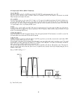
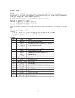
Rec Mode
¤˝
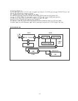
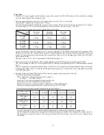
When Rec "H" signal is applied, Audio Head (Rec) point will be opened (EE & PB: GND) and coil will be oscillated by switching
circuit for High voltage and then starting rec. mode.
¤˛
Electronic potential difference between Vcc (5V) and pin #3 has to be in 2.0-4.3V to coil oscillate.
In other words, Voltage of pin #3 has to be in 0.7~3.0V p-p.
Specially if Head impedance of R/P and FE is center level, the voltage of Pin #3 has to be 1.85Vp-p consistantly. Pin #3 might be
over control range 0.7~3.0Vp-p when Head impedance is either max. or min. level unless Pin #3 is 1.85Vp-p.
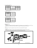
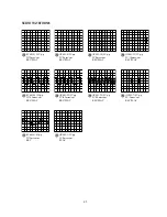
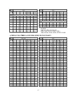
* Head Impedance Variation Owing to the Variation of Pin port 3 Voltage.
As you see from above chart, the voltage of pin # 3 gose up if impedance of FE HEAD is higher and higer, Impedance of R/P
HEAD is lower & lower. DC voltage of Pin #3 includes AC signal components, this means that Auto Bias is operated. If it does not
include AC signal components, means that Auto Bais is not operated. And, pin # 4 is on/off output port of BIAS control TR (Q205)
which sticks in outside.
During Rec. mode V
BE
(0.7~0.8V) is output and EE & PB mode the voltage is 0.
¤ˇ
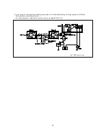
Audio signal out of pin # 64 through Rec AMP is mixed with Bias signal of 70 KHz components and then record in Head.
And, This signal input to inside of IC, when has 60KHz HPF so filtering Audio signal and pass only 70KHz components, through
Pin # 1.
Then it is compared by comparator (Standard Voltage is 320 mVrms). If it is bigger or smaller than standard Voltage, the compara-
tor Changes the voltage of Pin #3. So that, the BIAS signal which input to pin # 1 is always 320 mVrms. Bias signal has a tolerane
±10% (288-352mVrms)
¤—
Recording current is decided by BIAS signal of 320mVrms and resistance amount between pin # 64 and 1.
* The way of recording current estimation
BIAS = 320mVrms
¡
(Resistance between Pin 64 and Pin 1)
ex) 320mV
¡
1.3K OHM = 246µA
In this case, G-level resistor, which has less error has to be used.
Recording current can be controlled by resistance amount.
But if you use too much or too little resistane, it could be cause of bias signal defection.
Usually, the resistance amount between pin # 64 and 1 has to be in 1.0~2.2K OHM
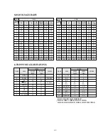
* The variation owing to the variation of resistance between pin 64 and pin 1.
As you see above chart, It is easy to find that the BIAS signal always in a tolerane range regardless of resistance Amt.
And the Change of Recording current is proportional to resistance Amt when a resistance Amt is changed, The voltage of pin #3 is
also changed, you can controll to make 1.85 Vp-p using R 207 and R208. The resistance is lower & lower, the voltage of pin #3
will gose up.
R/P
67K OHM
58K OHM
49K OHM
FE
(+15%)
(CENTER)
(–15%)
92 OHM
1.6Vp-p
1.9Vp-p
2.3Vp-p
(+15%)
80 OHM
1.4Vp-p
1.8Vp-p
2.1Vp-p
(CENTER)
68 OHM
1.1Vp-p
1.5vp-p
1.9Vp-p
(–15%)
Resistance between
1.0K OHM
1.3K OHM
1.5K OHM
1.8K OHM
2.2K OHM
Pin 64 and Pin 1.
BIAS signal
316
318
312
315
310
(mVrms)
Voltage of Pin 3
1.18
1.82
2.18
2.60
2.86
(V)
Rec. current
310
243
211
181
148
(µA)
Содержание DV- K584N-SJ
Страница 35: ...34 AC001 K584NZ SJ M K584NZ SG M only...
Страница 36: ...35...
Страница 37: ...36...
Страница 38: ...37...
Страница 39: ...38...
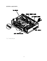
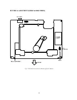
Страница 60: ...59 ELECTRICAL ADJUSTMENTS Fig 1 Circuit Board Location...
Страница 92: ...91 INTERCONNECT WIRING DIAGRAM K584N K484N K384N K284N...
Страница 93: ...92 POWER SUPPLY SCHEMATIC DIAGRAM FREE VOLTAGE K584NY SJ M K584NZ SJ M K584NZ SG M...
Страница 95: ...94 2HD HEAD AMP SCHEMATIC DIAGRAM K384N K284N K304N...
Страница 96: ...95 4HD HEAD AMP SCHEMATIC DIAGRAM K584N K484N K504N...
Страница 97: ...96 VIDEO AUDIO SCHEMATIC DIAGRAM K584N K484N K384N K284N K504N K304N...
Страница 98: ...97 PIF INPUT SELECTOR SCHEMATIC DIAGRAM 9V USE K584NY SJ M K584NZ SJ M K584NZ SG M...
Страница 100: ...99 TIMER SYSCON SCHEMATIC DIAGRAM K584N K484N K384N K284N K504N K304N...
Страница 101: ...100 POWER SUPPLY BLOCK DIAGRAM FREE VOLTAGE K584NY SJ M K584NZ SJ M K584NZ SG M...
Страница 103: ...102 2HD HEAD AMP BLOCK DIAGRAM K384N K284N K304N...
Страница 104: ...103 4HD HEAD AMP BLOCK DIAGRAM K584N K484N K504N...
Страница 105: ...104 VIDEO AUDIO BLOCK DIAGRAM K584N K484N K384N K284N K504N K304N...
Страница 106: ...105 PIF INPUT SELECTOR BLOCK DIAGRAM K584N K484N K384N K284N K504N K304N...
Страница 107: ...106 SYSCON SERVO BLOCK DIAGRAM K584N K484N K384N K284N K504N K304N SEG A SEG L SEG A SEG L SEG C SEG F G1 G8 G1 G8...
Страница 109: ...108 MAIN PCB 2HEAD 4HEAD...


