CDB4923 CDB49300
DS262DB2
5
1. CDB4923 VS. CDB49300
The CDB4923 and CDB49300 are two customer
development boards built from a single platform -
the CDB4923/300. This development board replac-
es the CDB4923 Rev. A and Rev. B.
Although the CDB4923/CDB49300 boards look
very similar, it is important to be aware that when
shipped from the factory, the CDB4923 is config-
ured for only the CS4923 family of audio decoders
and the CDB49300 is configured only for the
CS49300 family of audio decoders.
The features distinguishing the two boards are the
following:
•
DSP Power Setting
•
DSP PLL Filter Topology
1.1
DSP Power
The CS4923 family is designed to operate with a
core voltage of +3.3 V, and the CDB4923 is
shipped with the DSP Power jumper in the +3.3 V
position. The CS49300 family is designed to oper-
ate with a core voltage of +2.5 V, and the
CDB49300 is shipped with the DSP Power jumper
in the +2.5 V position. Attempting to use an audio
decoder on the wrong board (e.g., CS49300 on a
CDB4923) can cause unpredictable results and
damage the decoder.
1.2
DSP PLL Filter
The PLL of the CS4923 is different than that of the
CS49300. Consequently, the optimized external
PLL filters for each family of audio decoders is dif-
ferent. The CDB4923 is optimized for the CS4923
family and the CDB49300 is optimized for the
CS49300 family. Attempting to use an audio de-
coder on the wrong board (e.g., CS49300 on a
CDB4923) can cause unpredictable results.
Specifically, the relevant PLL filter components
for the CDB4923 are:
•
R246 = 0
Ω
•
C155 = 0.22
µ
F
The relevant PLL filter components for the
CDB49300 are:
•
R246 = 33 k
Ω
•
C155 = 0.22
µ
F
•
C113 = 0.01
µ
F
Although the boards are tailored for one specific
family of audio decoders, the operation of the
CDB4923 and CDB49300 is effectively the same.
This document will generically refer to the
CDB4923/300 except in those instances where
there is a difference between the boards.
2. OPERATION
The CDB4923/300 is designed to allow full evalu-
ation of the CS4923 family and CS49300 family of
audio DSPs. The members of each audio decoder
family are electrically equivalent, so it is possible
to use any member of the CS4923 family in the
CDB4923 and any member of the CS49300 family
in the CDB49300. In the context of this document,
CS492x should be interpreted as any member of the
CS4923 family and CS493xx should be understood
to be any member of the CS49300 family.
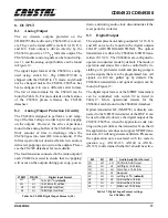
The CDB4923/300 is composed of 8 distinct re-
gions: DSP, Control Interface, Control Logic,
Clocks, Analog I/O, Digital I/O, Patch area, and
Power. Each board region has a number of compo-
nents and will be briefly discussed below. A more
thorough description of each will be given in dedi-
cated sections of this document which can be
quickly located in the Table of Contents.
The DSP section includes the audio decoder
(CS492x Multichannel Audio Decoder or CS493xx
Universal Audio Decoder) under evaluation, jump-
ers for controlling DSP power and DSP configura-
tion pins, and stake headers which provide access
to all relevant DSP pins. The jumpers allow the
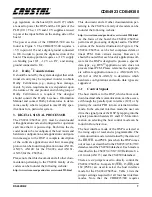
user to select b2.5 V or +3.3 V on the DSP
power pins (pre-configured at the factory for the
Содержание CS492 Series
Страница 18: ...CDB4923 CDB49300 18 DS262DB2 9 APPENDIX A SCHEMATICS Figure 4 CS492x CS493xx ...
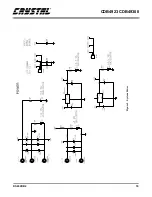
Страница 19: ...CDB4923 CDB49300 DS262DB2 19 Figure 5 System Power ...
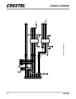
Страница 20: ...CDB4923 CDB49300 20 DS262DB2 Figure 6 PC Interface ...
Страница 21: ...CDB4923 CDB49300 DS262DB2 21 Figure 7 Control Logic ...
Страница 22: ...CDB4923 CDB49300 22 DS262DB2 Figure 8 Clocking ...
Страница 23: ...CDB4923 CDB49300 DS262DB2 23 Figure 9 Analog Input ...
Страница 24: ...CDB4923 CDB49300 24 DS262DB2 Figure 10 Digital Input ...
Страница 25: ...CDB4923 CDB49300 DS262DB2 25 Figure 11 D A Converters ...
Страница 26: ...CDB4923 CDB49300 26 DS262DB2 Figure 12 Analog Output ...
Страница 27: ...CDB4923 CDB49300 DS262DB2 27 Figure 13 Digital Output ...
Страница 28: ...CDB4923 CDB49300 28 DS262DB2 Figure 14 Top Layer ...
Страница 29: ...CDB4923 CDB49300 DS262DB2 29 Figure 15 Bottom Layer ...
Страница 30: ...CDB4923 CDB49300 30 DS262DB2 Figure 16 SSTOP ...
Страница 31: ...CDB4923 CDB49300 DS262DB2 31 Figure 17 ASYSTOP ...
Страница 32: ...CDB4923 CDB49300 32 DS262DB2 Figure 18 Layer 2 ...
Страница 33: ...CDB4923 CDB49300 DS262DB2 33 Figure 19 Layer 3 ...
Страница 49: ... Notes ...
Страница 50: ......


