background image

                                                                                                                         1

1.0 s a f e t y   a n d   s e r v i c i n g   n o t e s

1.1

Safety precautions

1. This unit is Class II, which means that it is not connected to the protective earth system.

All live voltages are insulated from the case by double insulation. 

2. Do not attempt to service unless qualified to do so.

3. Disconnect unit from AC power supply before removing cover.

4. Components marked with the        symbol on the circuit schematic are safety critical 

and must only be replaced with an identical component, or an alternative approved by
the manufacturer.

5. Switch unit off, and disconnect from supply before making and breaking any

connections.

6. Do not adjust any controls unless instructed to do so in this manual.

1.2

Electrostatic discharge precautions

Electrostatic discharge (ESD) is due to charges produced by insulating materials rubbing together.
Humans collect electrostatic charge through normal activities when clothes rub together and when
walking on carpet. This charge may be discharged suddenly when you touch a conductor. If the
conductor is connected to a sensitive electronic circuit, you may damage the components. It is also
possible to reduce the life of components without causing any obvious damage.

To prevent ESD damage, it is necessary to follow these guidelines.

1. Prepare work area. Place an ESD protective mat on the bench, strapped to the

protective earth circuit.

2. Prepare yourself. Put on an ESD protective wrist band, strapped to the protective earth

circuit, or to the ESD protective mat.

3. Keep all PCBs removed from unit in ESD protective bags.

4. Keep all replacement electronic components, PCBs and stock items in ESD protective

bags or boxes.

5. Be particularly careful with components marked with the following symbol:

1.3

Soldering

How to de-solder components

Components should be removed, wherever possible, using a de-soldering tool. Be careful not to
damage tracks and pads by applying too much pressure.

How to make good solder joints

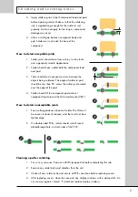
1. Ensure surfaces are clean.

2. Keep soldering iron clean and wetted with solder. Use an appropriate bit. Do not leave

soldering iron on when not in use.

Содержание 8000S

Страница 1: ...service manual Integrated amplifier 8000S ...

Страница 2: ...6701 07 02 18 7 3 Line amplifier right channel schematic SCH26701 08 02 19 7 4 Power amplifier left channel schematic SCH26701 09 02 20 7 5 Power amplifier right channel schematic SCH26701 10 02 21 7 6 Power supplies schematic SCH26701 01 02 22 7 7 Protect and turn on schematic SCH26701 06 02 23 7 8 Digital system controller schematic SCH26701 02 01 24 7 9 Digital system interface schematic SCH267...

Страница 3: ...et This charge may be discharged suddenly when you touch a conductor If the conductor is connected to a sensitive electronic circuit you may damage the components It is also possible to reduce the life of components without causing any obvious damage To prevent ESD damage it is necessary to follow these guidelines 1 Prepare work area Place an ESD protective mat on the bench strapped to the protect...

Страница 4: ...older to pad should be less than 90 unless the solder joint extends over the edge of the pad 4 Solder should fill the component pad and wet component lead around the full circumference 360 How to detect unacceptable joints 1 Poor wetting produces a bead of solder The fillet will be convex instead of concave and there will not be a feather edge 2 On double sided PCBs solder should wet all round pla...

Страница 5: ...ections RECORD SELECTOR INPUT SELECTOR MODE SWITCH VOLUME CONTROL HEADPHONE SOCKET POWER SWITCH POWER LED RED Power On MUTE LED RED Mute On REMOTE CONTROL SENSOR LOUDSPEAKER TERMINALS MAINS INPUT RIGHT LEFT FUSE HOLDER POWER AMPLIFIER INPUT PRE AMPLIFIER OUTPUTS TAPE 2 TAPE 1 VCR AUX CDR ETC CD DVD ...

Страница 6: ...em 4 1 Test equipment required Equipment Digital Multimeter Dual Tracking DC Power Supply Various Leads Specification Accuracy better than 0 5 in V and mV ranges Output 32 V DC 2 A Positive terminal of negative supply must be connected to negative terminal of the positive supply unless internally linked V mA V mA ve ve ve ve Select Tracking 0 V 32 V 32 V Black ve Red ve Green 0 V Figure 4 1 Functi...

Страница 7: ...ted supply Fuse Type 230 V AC T2 5A L250V 115 V AC T4A 125V 110 V AC T4A 125V Fuse and spare fuse should be low resistance Set output voltage to 32 V current limited to 500 mA With supplies off connect positive output of supply to positive terminal of reservoir capacitor negative output of supply to negative terminal of capacitor No connection is required to 0 V terminal of power supply CAUTION Do...

Страница 8: ...0 Connect positive probe to 30 V test point TP 19 Voltage should be 28 V 3 V Connect positive probe to 10 V test point TP 15 Voltage should be 10 V 0 3 V Connect positive probe to 5 V test point TP 16 Voltage should be 5 V 0 3 V Measure voltage across R731 TP 5 and TP 5 Voltage should be 0 85 V 0 1 V Measure voltage across R735 TP 6 and TP 6 Voltage should be 0 85 V 0 1 V Connect negative probe to...

Страница 9: ...mV If any faults have been detected repair and return to the beginning of this test procedure Measure volatge across D713 TP 1 and TP 1 and D714 TP 2 and TP 2 Volatge should be 44 V 2 5 V Measure volatge across D813 TP 3 and TP 3 and D814 TP 4 and TP 4 Volatge should be 44 V 2 5 V Connect negative probe to 0 V TP 0 Connect positive probe to cathode of D951 TP 23 Switch on AC power button Voltage s...

Страница 10: ...0 V TP 0 Connect positive probe to R749 TP 9 Voltage should be 5 mV Connect positive probe to R518 TP 12 Voltage should be 14 V 1 V Measure voltage across R831 TP 7 and TP 7 Voltage should be 0 85 V 0 1 V Measure voltage across R835 TP 8 and TP 8 Voltage should be 0 85 V 0 1 V Connect negative probe to 0 V TP 0 Connect positive probe to R849 TP 10 Voltage should be 5 mV Connect positive probe to R...

Страница 11: ...io greater than 95 dB with IHF A weighted filter 20 MHz dual channel 8 Ω 125 W and short circuit 2 off Equipment True RMS multimeter Audio analyser Oscilloscope Output loads Shorted phono plugs Various leads Figure 5 1 Performance test set up Connections for left channel shown repeat connections for right channel 8 Ω Load AC Power Input Oscilloscope Audio analyser Output Input Ch 1 Ch 2 CD I P Sco...

Страница 12: ...tput 1kHz 1 V rms 200Hz HP filter on A weighted filter off Audio Analyser output 1kHz 1 V rms 200Hz HP filter on A weighted filter off Details Output frequency 1 kHz sine wave Output voltage 100 mV rms Reading settings AC level Auto 200 Hz HP filter on A weighted filter off Select cd using INPUT selector knob Select pre using MODE selector knob Measure output of left and right PRE AMP sockets Volt...

Страница 13: ...r ch1 Details Adjust VOLUME knob until voltage on output of amplifier is 2 83 V rms or 1 W If possible set this as 0 dB reference Remove input leads and replace with shorted phono plugs Measure dB reading if function is available which is equivalent to signal to noise ratio Alternatively measure noise voltage and calculate SNR SNR should be 80 dB SNR 10 log10 signal power noise power SNR 20 log10 ...

Страница 14: ... with Figure 5 2 Trace will appear briefly and will disappear when amplifier mutes Disconnect input signal and loudspeaker leads Turn VOLUME knob to 12 o clock Connect negative probe to 0 V TP 0 Connect positive probe to input socket signal pin TP 21 Make sure amplifier mutes Disconnect positive probe Make sure mute relay resets not muted Relay will click Connect positive probe to 0 V TP 0 Connect...

Страница 15: ...ck operation of remote controller Clean with damp cloth Test Equipment Multimeter set to diode test Connect to CD player and preamplifier and play a TAG McLaren Audio Test Tracks CD Details Connect positive probe to 0 V TP 0 Connect negative probe to input socket signal pin TP 22 Make sure amplifier mutes Disconnect positive probe Make sure mute relay resets not muted Relay will click Remove all l...

Страница 16: ... n t s 6 1 Functional and performance test points TP 7 TP 4 TP 1 TP 0 TP 16 TP 15 TP 19 TP 3 TP 3 TP 10 TP 11 TP 4 TP 25 TP 9 TP 8 TP 8 TP 6 TP 6 TP 5 TP 5 TP 12 TP 13 TP 1 TP 2 TP 2 TP 24 TP 0 TP 0 TP 7 TP 23 TP 22 TP 21 ...

Страница 17: ...7 SCH26701 02 01 PAGE 24 SCH26701 03 01 PAGE 25 SCH26701 04 04 PAGE 26 SCH26703 01 01 PAGE 29 SCH26701 10 02 PAGE 21 SCH26701 09 02 PAGE 20 SCH26701 06 02 PAGE 23 SCH26701 01 02 PAGE 22 SCH26701 08 02 PAGE 19 SCH26701 07 02 PAGE 18 TP 21 TP 22 7 1 1 Master schematic diagram SCH267M 01 05 ...

Страница 18: ...0V 14 4V 14 0V 4 1V 4 7V 14 6V 28 8V 28 8V 0 4V 0 4V 1 0V 29 0V 0 0V 28 8V 28 2V 28 8V 28 2V 30 0V TP 12 All DC voltages are relative to 0 V Measurements should be made with no connections to amplifier except AC power Use high input impedance voltmeter 20 kΩ V Meter must be floating relative to ground ...

Страница 19: ...0 0V 0 0V 14 4V 28 2V 14 0V 4 7V 0 4V 0 4V 1 0V 28 8V 30 0V 28 8V 29 0V 4 1V 28 8V 28 2V 14 6V 28 8V TP 13 All DC voltages are relative to 0 V Measurements should be made with no connections to amplifier except AC power Use high input impedance voltmeter 20 kΩ V Meter must be floating relative to ground ...

Страница 20: ... TP 5 TP 5 TP 2 TP 24 TP 6 TP 6 TP 2 TP 1 TP 9 TP 1 20 1 7 0 c i rc u i t s c h e m a t i c s 7 4 1 Power amplifier left channel schematic SCH26701 09 02 All DC voltages are relative to 0 V Measurements should be made with no connections to amplifier except AC power Use high input impedance voltmeter 20 kΩ V Meter must be floating relative to ground ...

Страница 21: ...2 4V 12 0V 43 0V 41 8V 8 0V 11 6V 12 0V 42 4V 43 0V 41 8V 11 6V 10 3V 11 5V 11 5V 10 9V 44 0V 44 0V TP 7 TP 7 TP 4 TP 25 TP 8 TP 8 TP 4 TP 3 TP 10 TP 3 All DC voltages are relative to 0 V Measurements should be made with no connections to amplifier except AC power Use high input impedance voltmeter 20 kΩ V Meter must be floating relative to ground ...

Страница 22: ...0V 5 0V 6 2V 6 8V 28 8V 6 2V 10 0V 30 0V 0 0V 0 0V 6 8V 30 0V 6 2V TP 17 TP 15 TP 19 TP 16 TP 18 TP 0 All DC voltages are relative to 0 V Measurements should be made with no connections to amplifier except AC power Use high input impedance voltmeter 20 kΩ V Meter must be floating relative to ground ...

Страница 23: ... 44 0V 0 0V 0 0V 44 0V 44 0V 0 0V 0 0V 0 0V 0 0V 22 2V 44 0V 44 0V 28 1V 12 0V 0 0V 0 0V 0 0V 44 0V 18 0V 0 0V 44 0V 0 0V TP 11 TP 23 ZTX753 ZTX653 All DC voltages are relative to 0 V Measurements should be made with no connections to amplifier except AC power Use high input impedance voltmeter 20 kΩ V Meter must be floating relative to ground ...

Страница 24: ...24 7 0 c i rc u i t s c h e m a t i c s 7 8 Digital system controller schematic SCH26701 02 01 ...

Страница 25: ...25 7 0 c i rc u i t s c h e m a t i c s 7 9 Digital system interface schematic SCH26701 03 01 ...

Страница 26: ...26 1 7 0 c i rc u i t s c h e m a t i c s 7 10 1 Input interface schematic SCH26701 04 04 BZV86 2V0 ...

Страница 27: ...27 7 0 c i rc u i t s c h e m a t i c s 7 11 Relay coils schematic SCH26701 05 01 ...

Страница 28: ...28 7 0 c i rc u i t s c h e m a t i c s 7 12 Front panel schematic SCH26702 01 01 ...

Страница 29: ...29 7 0 c i rc u i t s c h e m a t i c s 7 13 Speaker outputs schematic SCH26703 01 01 ...

Страница 30: ... digital system controller digital system interface power amplifier right channel power amplifier left channel protect turn on delay power supply power supply input interface digital system controller power supply 8 1 Printed circuit board layout top view ...

Страница 31: ...digital system controller digital system interface power amplifier right channel power amplifier left channel protect turn on delay power supply power supply input interface digital system controller power supply 8 2 Printed circuit board layout bottom view ...

Страница 32: ...B i e the record output level is the same as the input level 47 kΩ nominal 782 mV rms for full rated output 29 0 dB at 1 kHz greater than 80 dB relative to 0 dBW 1 Hz 65 kHz rated output power both channels driven typical output power both channels driven preamplifier input impedance preamplifier input level preamplifier gain preamplifier signal to noise power amplifier gain record output impedanc...

Страница 33: ...5 C 50 60 Hz 110 120 V or 220 240 V The voltage is marked on the rear of the unit less than 300 W 445 mm wide 75 mm high 350 mm deep channel seperation crosstalk rejection polarity phase headphone output impedance operating temperature range ac supply frequency ac supply voltage power consumption The rated and typical performance applies when the mains supply voltage is either 230 V AC for 220 240...

Страница 34: ... by 93 23 EEC 73 23 EEC Low Voltage Directive as amended by 93 23 EEC IEC65 1985 IEC65 A2 1989 IEC65 A3 1992 EN60065 1993 EN50081 1 1992 EN55022 Class B 1994 EN60555 2 1987 EN61000 3 2 1995 EN61000 3 3 1995 FCC Part 15 Class B 1997 EN50082 1 1992 IEC801 2 1991 8 kV air discharge IEC801 3 1984 3 V m IEC801 4 1988 1 kV AC power 500 V other ports EN61000 4 2 1995 8 kV air 4 kV contact discharge EN610...

Страница 35: ...IAG Service Centre Unit 4 St Margaret s Way Stukeley Meadows Industrial Estate Huntingdon Cambs PE29 6EB England ephone 452561 13403 www audiolab co uk Tel 44 0 1480 Fax 44 0 1480 ...

Отзывы: