Specifications
ARM DUI 0447J
Copyright © 2009-2014, ARM. All rights reserved.
B-5
ID052914
Non-Confidential
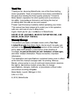
Figure B-4 Asynchronous write timing
The intervals are as follows:
•
Tsmbis
= 6ns
•
Tsmbov
= 7.5ns
•
Tsmbfis
= 6ns
•
Tsmbfov
= 6ns
•
Tsmboh
=
Tperiod
/2
All SMB input signals are registered on the rising edge of
SMB_CLKO
. They are then
registered a second time before being output on the IOFPGA SMB bus. This adds 1.5 clock
cycles of latency.
All IOFPGA SMB input signals are registered on the rising edge of
SMB_CLKO
. They are
then registered a second time before being output to the SMB bus. This adds 2 clock cycles of
latency.
An asynchronous write therefore has a penalty of 1.5 clock cycles because of going though the
IO FPGA.
B.1.5
Video multiplexer FPGA timing
Figure B-5 on page B-6
shows the video multiplexer FPGA timing.
WDATA
SMB_DATA
SMB_nWE
SMB_nCS
SMB_ADDR
ADDR
SMB_CLKO
SMB_nCSreg_in
SMBF_nCS
SMBF_DATA
WDATA
SMBF_DATAreg_in
WDATA
SMBF_DATA
SMBF_nWE
Tsmb
is
Trc
Tsmb
is
Tsmb
ov
Tsmb
ov
Tsmb
ov
Tsmb
ov