background image

C3.4 

AMU events

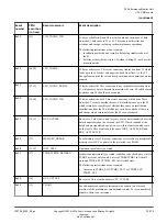
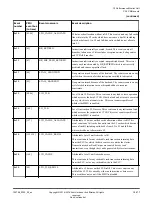
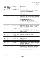
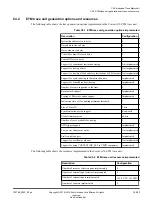
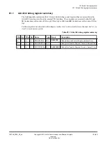
The following table describes the counters that are implemented in the Cortex-A76 core and the mapping
to fixed and programmable events.

Table C3-1  Mapping of counters to fixed events

Activity
monitor
counter <n>

Event
type

Event

Event
number

Description

0

Fixed

Cycles at core
frequency

0x11

Cycles count.

1

Fixed

Cycles at constant
frequency

0xEF

This counter is used to replicate the generic system counter that is
incremented on a constant basis, and not incremented depending on
the PE frequency core.

2

Fixed

Instructions retired

0x08

Instruction architecturally executed. This counter increments for
every instruction that is executed architecturally, including
instructions that fail their condition code check.

3

Fixed

First miss

0xF0

The first miss event tracks whether any external load miss is
outstanding and starts counting only from a first-miss until data
returns for that miss. The counter does not count for any remaining
part of overlapping accesses, only counting again when the first-
miss condition is re-detected.

4

Fixed

High activity

0xF1

Instructions executing through the design which act as a hint for
potential high power activity.

C3 Activity Monitor Unit

C3.4 AMU events

100798_0300_00_en

Copyright © 2016–2018 Arm Limited or its affiliates. All rights

reserved.

C3-389

Non-Confidential

Содержание Cortex-A76 Core

Страница 1: ...Arm Cortex A76 Core Revision r3p0 Technical Reference Manual Copyright 2016 2018 Arm Limited or its affiliates All rights reserved 100798_0300_00_en ...

Страница 2: ...T NOT PROHIBITED BY LAW IN NO EVENT WILL ARM BE LIABLE FOR ANY DAMAGES INCLUDING WITHOUT LIMITATION ANY DIRECT INDIRECT SPECIAL INCIDENTAL PUNITIVE OR CONSEQUENTIAL DAMAGES HOWEVER CAUSED AND REGARDLESS OF THE THEORY OF LIABILITY ARISING OUT OF ANY USE OF THIS DOCUMENT EVEN IF ARM HAS BEEN ADVISED OF THE POSSIBILITY OF SUCH DAMAGES This document consists solely of commercial items You shall be res...

Страница 3: ...cordance with the terms of the agreement entered into by Arm and the party that Arm delivered this document to Unrestricted Access is an Arm internal classification Product Status The information in this document is Final that is for a developed product Web Address http www arm com Arm Cortex A76 Core 100798_0300_00_en Copyright 2016 2018 Arm Limited or its affiliates All rights reserved 3 Non Con...

Страница 4: ......

Страница 5: ... A1 29 A1 5 Test features A1 30 A1 6 Design tasks A1 31 A1 7 Product revisions A1 32 Chapter A2 Technical overview A2 1 Components A2 34 A2 2 Interfaces A2 38 A2 3 About system control A2 39 A2 4 About the Generic Timer A2 40 Chapter A3 Clocks resets and input synchronization A3 1 About clocks resets and input synchronization A3 42 A3 2 Asynchronous interface A3 43 100798_0300_00_en Copyright 2016...

Страница 6: ...stem A6 77 A6 5 Data prefetching A6 79 A6 6 Direct access to internal memory A6 80 Chapter A7 Level 2 memory system A7 1 About the L2 memory system A7 98 A7 2 About the L2 cache A7 99 A7 3 Support for memory types A7 100 Chapter A8 Reliability Availability and Serviceability RAS A8 1 Cache ECC and parity A8 102 A8 2 Cache protection behavior A8 103 A8 3 Uncorrected errors and data poisoning A8 105...

Страница 7: ...3 B2 21 CPTR_EL2 Architectural Feature Trap Register EL2 B2 164 B2 22 CPTR_EL3 Architectural Feature Trap Register EL3 B2 165 B2 23 CPUACTLR_EL1 CPU Auxiliary Control Register EL1 B2 166 B2 24 CPUACTLR2_EL1 CPU Auxiliary Control Register 2 EL1 B2 168 B2 25 CPUCFR_EL1 CPU Configuration Register EL1 B2 170 B2 26 CPUECTLR_EL1 CPU Extended Control Register EL1 B2 172 B2 27 CPUPCR_EL3 CPU Private Contr...

Страница 8: ...tion Set Attribute Register 1 EL1 B2 235 B2 67 ID_ISAR2_EL1 AArch32 Instruction Set Attribute Register 2 EL1 B2 237 B2 68 ID_ISAR3_EL1 AArch32 Instruction Set Attribute Register 3 EL1 B2 239 B2 69 ID_ISAR4_EL1 AArch32 Instruction Set Attribute Register 4 EL1 B2 241 B2 70 ID_ISAR5_EL1 AArch32 Instruction Set Attribute Register 5 EL1 B2 243 B2 71 ID_ISAR6_EL1 AArch32 Instruction Set Attribute Regist...

Страница 9: ...registers B4 1 CPU interface registers B4 313 B4 2 AArch64 physical GIC CPU interface system register summary B4 314 B4 3 ICC_AP0R0_EL1 Interrupt Controller Active Priorities Group 0 Register 0 EL1 B4 315 B4 4 ICC_AP1R0_EL1 Interrupt Controller Active Priorities Group 1 Register 0 EL1 B4 316 B4 5 ICC_BPR0_EL1 Interrupt Controller Binary Point Register 0 EL1 B4 317 B4 6 ICC_BPR1_EL1 Interrupt Contr...

Страница 10: ... About debug methods C1 366 C1 2 Debug register interfaces C1 367 C1 3 Debug events C1 369 C1 4 External debug interface C1 370 Chapter C2 Performance Monitor Unit C2 1 About the PMU C2 372 C2 2 PMU functional description C2 373 C2 3 PMU events C2 374 C2 4 PMU interrupts C2 383 C2 5 Exporting PMU events C2 384 Chapter C3 Activity Monitor Unit C3 1 About the AMU C3 386 C3 2 Accessing the activity m...

Страница 11: ...ance Monitors Common Event Identification Register 0 D4 436 D4 3 PMCEID1 Performance Monitors Common Event Identification Register 1 D4 439 D4 4 PMCR Performance Monitors Control Register D4 441 Chapter D5 AArch64 PMU registers D5 1 AArch64 PMU register summary D5 446 D5 2 PMCEID0_EL0 Performance Monitors Common Event Identification Register 0 EL0 D5 448 D5 3 PMCEID1_EL0 Performance Monitors Commo...

Страница 12: ... Register D9 502 D9 5 TRCAUXCTLR Auxiliary Control Register D9 503 D9 6 TRCBBCTLR Branch Broadcast Control Register D9 505 D9 7 TRCCCCTLR Cycle Count Control Register D9 506 D9 8 TRCCIDCCTLR0 Context ID Comparator Control Register 0 D9 507 D9 9 TRCCIDCVR0 Context ID Comparator Value Register 0 D9 508 D9 10 TRCCIDR0 ETM Component Identification Register 0 D9 509 D9 11 TRCCIDR1 ETM Component Identif...

Страница 13: ...eripheral Identification Register 1 D9 565 D9 56 TRCPIDR2 ETM Peripheral Identification Register 2 D9 566 D9 57 TRCPIDR3 ETM Peripheral Identification Register 3 D9 567 D9 58 TRCPIDR4 ETM Peripheral Identification Register 4 D9 568 D9 59 TRCPIDRn ETM Peripheral Identification Registers 5 7 D9 569 D9 60 TRCPRGCTLR Programming Control Register D9 570 D9 61 TRCRSCTLRn Resource Selection Control Regis...

Страница 14: ... 592 A 2 Load Store accesses crossing page boundaries Appx A 593 A 3 Armv8 Debug UNPREDICTABLE behaviors Appx A 594 A 4 Other UNPREDICTABLE behaviors Appx A 597 Appendix B Revisions B 1 Revisions Appx B 600 100798_0300_00_en Copyright 2016 2018 Arm Limited or its affiliates All rights reserved 14 Non Confidential ...

Страница 15: ... the Arm Cortex A76 Core Technical Reference Manual It contains the following About this book on page 16 Feedback on page 21 100798_0300_00_en Copyright 2016 2018 Arm Limited or its affiliates All rights reserved 15 Non Confidential ...

Страница 16: ...e clocks resets and input synchronization of the Cortex A76 core Chapter A4 Power management This chapter describes the power domains and the power modes in the Cortex A76 core Chapter A5 Memory Management Unit This chapter describes the Memory Management Unit MMU of the Cortex A76 core Chapter A6 Level 1 memory system This chapter describes the L1 instruction cache and data cache that make up the...

Страница 17: ...r D1 AArch32 debug registers This chapter describes the debug registers in the AArch32 Execution state and shows examples of how to use them Chapter D2 AArch64 debug registers This chapter describes the debug registers in the AArch64 Execution state and shows examples of how to use them Chapter D3 Memory mapped debug registers This chapter describes the memory mapped debug registers and shows exam...

Страница 18: ...ames and source code monospace Denotes a permitted abbreviation for a command or option You can enter the underlined text instead of the full command or option name monospace italic Denotes arguments to monospace text where the argument is to be replaced by a specific value monospace bold Denotes language keywords when used outside example code and Encloses replaceable terms for assembler syntax w...

Страница 19: ...Shared Unit Integration Manual 100455 Arm DynamIQ Shared Unit Technical Reference Manual 100453 Arm DynamIQ Shared Unit Configuration and Sign off Guide 100454 Arm CoreSight ELA 500 Embedded Logic Analyzer Technical Reference Manual 100127 AMBA AXI and ACE Protocol Specification AXI3 AXI4 and AXI4 Lite ACE and ACE Lite IHI 0022 AMBA APB Protocol Version 2 0 Specification IHI 0024 Arm AMBA 5 CHI Ar...

Страница 20: ...minology is largely based on the earlier ANSI IEEE Std 754 1985 issue of the standard See the Arm Architecture Reference Manual Armv8 for Armv8 A architecture profile for more information Preface Additional reading 100798_0300_00_en Copyright 2016 2018 Arm Limited or its affiliates All rights reserved 20 Non Confidential ...

Страница 21: ...a arm com Give The title Arm Cortex A76 Core Technical Reference Manual The number 100798_0300_00_en If applicable the page number s to which your comments refer A concise explanation of your comments Arm also welcomes general suggestions for additions and improvements Note Arm tests the PDF only in Adobe Acrobat and Acrobat Reader and cannot guarantee the quality of the represented document when ...

Страница 22: ......

Страница 23: ...Part A Functional description ...

Страница 24: ......

Страница 25: ...on page A1 26 A1 2 Features on page A1 27 A1 3 Implementation options on page A1 28 A1 4 Supported standards and specifications on page A1 29 A1 5 Test features on page A1 30 A1 6 Design tasks on page A1 31 A1 7 Product revisions on page A1 32 100798_0300_00_en Copyright 2016 2018 Arm Limited or its affiliates All rights reserved A1 25 Non Confidential ...

Страница 26: ...el 1 L1 memory system and a private integrated Level 2 L2 cache It also includes a superscalar variable length out of order pipeline The Cortex A76 core is implemented inside the DynamIQ Shared Unit DSU cluster For more information see the Arm DynamIQ Shared Unit Technical Reference Manual The following figure shows an example of a configuration with four Cortex A76 cores External memory interface...

Страница 27: ...nnect to an external distributor Generic Timers interface supporting 64 bit count input from an external system counter Reliability Availability and Serviceability RAS Extension Cache features Separate L1 data and instruction caches Private unified data and instruction L2 cache Optional L1 and L2 memory protection in the form of Error Correcting Code ECC or parity on all RAM instances Debug featur...

Страница 28: ...bit This specifies the bus width between the core and the DSU CPU bridge The legal core bus width and master bus width combinations are If the core bus width is 128 bits the master bus interface can be any of the following options Single 128 bit wide ACE interface Dual 128 bit wide ACE interfaces Single 128 bit wide CHI interface Single 256 bit wide CHI interface If the core bus width is 256 bits ...

Страница 29: ...nsions The Cortex A76 core implements the LDAPR instructions introduced in the Armv8 3 A extensions The Cortex A76 core optionally implements the SDOT and UDOT instructions introduced in the Armv8 4 A extensions The Cortex A76 core implements the PSTATE Speculative Store Bypass Safe SSBS bit introduced in the Armv8 5 A extension Generic Interrupt Controller GICv4 Generic Timer Armv8 A 64 bit exter...

Страница 30: ...he use of both Automatic Test Pattern Generation ATPG and Memory Built In Self Test MBIST to test the core logic and memory arrays A1 Introduction A1 5 Test features 100798_0300_00_en Copyright 2016 2018 Arm Limited or its affiliates All rights reserved A1 30 Non Confidential ...

Страница 31: ... and initialize the core and tests the application software The operation of the final device depends on the following Build configuration The implementer chooses the options that affect how the RTL source files are pre processed These options usually include or exclude logic that affects one or more of the area maximum frequency and features of the resulting macrocell Configuration inputs The int...

Страница 32: ...nter Exception level isolation of branch predictor structures so that an Exception Level cannot train branch prediction for a different Exception Level to reliability hit in these trained prediction entries Implemented new barrier SSBB r3p0 Implemented new barriers PSSBB and CSDB Support for Speculative Store Bypass Safe SSBS bit enabling software to indicate whether hardware is permitted to load ...

Страница 33: ...e It contains the following sections A2 1 Components on page A2 34 A2 2 Interfaces on page A2 38 A2 3 About system control on page A2 39 A2 4 About the Generic Timer on page A2 40 100798_0300_00_en Copyright 2016 2018 Arm Limited or its affiliates All rights reserved A2 33 Non Confidential ...

Страница 34: ...see the Arm DynamIQ Shared Unit Technical Reference Manual The main components of the Cortex A76 core are Instruction fetch Instruction decode Register rename Instruction issue Execution pipelines L1 data memory system L2 memory system A2 Technical overview A2 1 Components 100798_0300_00_en Copyright 2016 2018 Arm Limited or its affiliates All rights reserved A2 34 Non Confidential ...

Страница 35: ...mory System ETM GIC CPU Interface DSU SCU and L3 Instruction Decode Register Rename Instruction Issue Commit Execution Pipeline MMU Load Store DSU Asynchronous Bridges This core is optional Figure A2 1 Cortex A76 core overview A2 Technical overview A2 1 Components 100798_0300_00_en Copyright 2016 2018 Arm Limited or its affiliates All rights reserved A2 35 Non Confidential ...

Страница 36: ...e The register rename unit performs register renaming to facilitate out of order execution and dispatches decoded instructions to various issue queues A2 1 4 Instruction issue The instruction issue unit controls when the decoded instructions are dispatched to the execution pipelines It includes issue queues for storing instruction pending dispatch to execution pipelines A2 1 5 Execution pipeline T...

Страница 37: ...apter A5 Memory Management Unit on page A5 61 Chapter A6 Level 1 memory system on page A6 71 Chapter A7 Level 2 memory system on page A7 97 Chapter A9 Generic Interrupt Controller CPU interface on page A9 111 Chapter C1 Debug on page C1 365 Chapter C2 Performance Monitor Unit on page C2 371 Chapter C4 Embedded Trace Macrocell on page C4 391 A2 Technical overview A2 1 Components 100798_0300_00_en C...

Страница 38: ...a SoC The DSU manages all interfaces For information on the interfaces see the Arm DynamIQ Shared Unit Technical Reference Manual A2 Technical overview A2 2 Interfaces 100798_0300_00_en Copyright 2016 2018 Arm Limited or its affiliates All rights reserved A2 38 Non Confidential ...

Страница 39: ... management Cache configuration and management System performance monitoring GIC configuration and management The system registers are accessible in the AArch64 EL0 EL3 and AArch32 EL0 Execution state Some of the system registers are accessible through the external debug interface A2 Technical overview A2 3 About system control 100798_0300_00_en Copyright 2016 2018 Arm Limited or its affiliates Al...

Страница 40: ...Secure physical timer A virtual timer A Hypervisor virtual timer The Cortex A76 core does not include the system counter This resides in the SoC The system counter value is distributed to the core with a 64 bit bus For more information on the Generic Timer see the Arm DynamIQ Shared Unit Technical Reference Manual and the Arm Architecture Reference Manual Armv8 for Armv8 A architecture profile A2 ...

Страница 41: ...input synchronization of the Cortex A76 core It contains the following sections A3 1 About clocks resets and input synchronization on page A3 42 A3 2 Asynchronous interface on page A3 43 100798_0300_00_en Copyright 2016 2018 Arm Limited or its affiliates All rights reserved A3 41 Non Confidential ...

Страница 42: ... These interfaces can be in the same clock domain or in other clock domains For information about clocks resets and input synchronization see the Arm DynamIQ Shared Unit Technical Reference Manual A3 Clocks resets and input synchronization A3 1 About clocks resets and input synchronization 100798_0300_00_en Copyright 2016 2018 Arm Limited or its affiliates All rights reserved A3 42 Non Confidentia...

Страница 43: ...tween the core and the DSU top level See the Arm DynamIQ Shared Unit Technical Reference Manual for more information A3 Clocks resets and input synchronization A3 2 Asynchronous interface 100798_0300_00_en Copyright 2016 2018 Arm Limited or its affiliates All rights reserved A3 43 Non Confidential ...

Страница 44: ...A3 Clocks resets and input synchronization A3 2 Asynchronous interface 100798_0300_00_en Copyright 2016 2018 Arm Limited or its affiliates All rights reserved A3 44 Non Confidential ...

Страница 45: ...mains on page A4 48 A4 4 Architectural clock gating modes on page A4 50 A4 5 Power control on page A4 52 A4 6 Core power modes on page A4 53 A4 7 Encoding for power modes on page A4 56 A4 8 Power domain states for power modes on page A4 57 A4 9 Power up and down sequences on page A4 58 A4 10 Debug over powerdown on page A4 59 100798_0300_00_en Copyright 2016 2018 Arm Limited or its affiliates All ...

Страница 46: ...y Scaling DVFS Static power management includes the following features Dynamic retention Powerdown Related references A4 3 Power domains on page A4 48 A4 8 Power domain states for power modes on page A4 57 A4 5 Power control on page A4 52 A4 9 Power up and down sequences on page A4 58 A4 Power management A4 1 About power management 100798_0300_00_en Copyright 2016 2018 Arm Limited or its affiliate...

Страница 47: ...c exists between the voltage domains The Cortex A76 core logic and core clock domain of the asynchronous bridge are in the VCPU voltage domain The DSU clock domain of the asynchronous bridge is in the VSYS voltage domain Note You can tie VCPU and VSYS to the same supply if one of the following conditions is met The core is configured to run synchronously with the DSU sharing the same clock The cor...

Страница 48: ...nt block the L1 and L2 TLBs L1 and L2 cache RAMs and Debug registers that are associated with the Cortex A76 core n is the number of Cortex A76 cores The number represents core 0 core 1 core 2 and core 3 If a core is not present the corresponding power domain is not present PDSYS Top level hierarchy and everything outside u_vcpu The domain is the interface between Cortex A76 and the DSU It contain...

Страница 49: ...y and the number of domains increases based on the number of Cortex A76 cores present This example only shows the power domains that are associated with the Cortex A76 cores other power domains are required for a DSU Cluster Core 3 L2 PDCPU 3 domain L1 Core 2 L2 PDCPU 2 domain L1 Core 1 L2 PDCPU 1 domain L1 Core 0 L2 PDCPU 0 domain L1 Adv SIMD FP Adv SIMD FP Adv SIMD FP Adv SIMD FP PDSYS Figure A4...

Страница 50: ...gisters residing in the core power domain A GIC CPU access through the AXI4 stream channel Exit from WFI low power state occurs when one of the following occurs The core detects one of the WFI wake up events The core detects a reset For more information see the Arm Architecture Reference Manual Armv8 for Armv8 A architecture profile A4 4 2 Core Wait for Event WFE is a feature of the Armv8 A archit...

Страница 51: ...ENTI input signal is asserted The core detects a reset For more information see the Arm Architecture Reference Manual Armv8 for Armv8 A architecture profile A4 Power management A4 4 Architectural clock gating modes 100798_0300_00_en Copyright 2016 2018 Arm Limited or its affiliates All rights reserved A4 51 Non Confidential ...

Страница 52: ... then performs any actions necessary to reach the requested power mode such as gating clocks flushing caches or disabling coherency before accepting the request If the request is not valid either because of an incorrect transition or because the status has changed so that state is no longer appropriate then the request is denied The power mode of each core can be independent of other cores in the ...

Страница 53: ...as a tie off for an unused P Channel it is an assumed transition from the Off mode This includes an invalidation of any cache RAM within the core domain A4 6 2 Off The Cortex A76 core supports a full shutdown mode where power can be removed completely and no state is retained The shutdown can be for either the whole cluster or just for an individual core which allows other cores in the cluster to ...

Страница 54: ...oming access proceeds when the domain is returned to On using P Channel When the incoming access completes and if the core has not exited WFI or WFE mode then the On PACTIVE bit is set LOW after the programmed retention timeout The power controller can then request to reenter the core dynamic retention mode A4 6 5 Debug recovery mode The debug recovery mode can be used to assist debug of external ...

Страница 55: ...hen these may complete after the reset when the core is not expecting them and cause a system deadlock A4 Power management A4 6 Core power modes 100798_0300_00_en Copyright 2016 2018 Arm Limited or its affiliates All rights reserved A4 55 Non Confidential ...

Страница 56: ...up Core dynamic retention FULL_RET 5 0b000101 Logic and RAM state are inoperable but retained Off emulated OFF_EMU 1 0b000001 On with Warm reset asserted debug state is retained and accessible Off OFF 0 implicit b 0b000000 All powerdown a PSTATE 5 4 are don t care b It is tied off to 0 and should be inferred when all other PACTIVE bits are LOW For more information see the AMBA Low Power Interface ...

Страница 57: ...hown in the following tables are unsupported and must not occur The following table describes the power modes and the corresponding power domain states for individual cores The power mode of each core is independent of all other cores in the cluster Table A4 4 Supported core power domain states Power mode Power domain state Description Debug recovery On Core on On On Core on Core dynamic retention...

Страница 58: ...e L3 memory system is performed in hardware after the WFI is executed under the direction of the power controller Note Executing any WFI instruction when the CPUPWRCTLR CORE_PWRDN_EN bit is set automatically masks out all interrupts and wake up events in the core If executed when the CPUPWRCTLR CORE_PWRDN_EN bit is set the WFI never wakes up and the core needs to be reset to restart For informatio...

Страница 59: ...ing to re establish a connection each time the core is powered up The debug over powerdown logic is part of the DebugBlock which is external to the cluster and must remain powered on during the debug over powerdown process See the Arm DynamIQ Shared Unit Technical Reference Manual A4 Power management A4 10 Debug over powerdown 100798_0300_00_en Copyright 2016 2018 Arm Limited or its affiliates All...

Страница 60: ...A4 Power management A4 10 Debug over powerdown 100798_0300_00_en Copyright 2016 2018 Arm Limited or its affiliates All rights reserved A4 60 Non Confidential ...

Страница 61: ... the MMU on page A5 62 A5 2 TLB organization on page A5 64 A5 3 TLB match process on page A5 65 A5 4 Translation table walks on page A5 66 A5 5 MMU memory accesses on page A5 67 A5 6 Specific behaviors on aborts and memory attributes on page A5 68 100798_0300_00_en Copyright 2016 2018 Arm Limited or its affiliates All rights reserved A5 61 Non Confidential ...

Страница 62: ...cts access to contiguous translation tables and prefetches the next one This prefetcher can be disabled in the ECTLR register The TLB entries contain either one or both of a global indicator and an Address Space Identifier ASID to permit context switches without requiring the TLB to be invalidated The TLB entries contain a Virtual Machine Identifier VMID to permit virtual machine switches by the h...

Страница 63: ... same behavior as EL1 See the Arm Architecture Reference Manual Armv8 for Armv8 A architecture profile for more information on concatenated translation tables and for address translation formats A5 Memory Management Unit A5 1 About the MMU 100798_0300_00_en Copyright 2016 2018 Arm Limited or its affiliates All rights reserved A5 63 Non Confidential ...

Страница 64: ... L1 TLBs The following table describes the characteristic that applies to the L2 TLB Table A5 3 Characteristic of the L2 TLB Characteristic Note 5 way set associative 1280 entry cache Stores VA to PA mappings for 4KB 16KB 64KB 2MB 32MB 512MB and 1GB block sizes Intermediate physical address IPA to PA mappings for 2MB and 1GB in a 4KB translation granule 32MB in a 16K translation granule and 512MB ...

Страница 65: ...0 in Non secure state A TLB match entry occurs when the following conditions are met Its VA moderated by the page size such as the VA bits 48 N where N is log2 of the block size for that translation that is stored in the TLB entry matches the requested address Entry translation regime matches the current translation regime The ASID matches the current ASID held in the CONTEXTIDR TTBR0 or TTBR1 reg...

Страница 66: ...he matching entry does not pass the permission checks the MMU signals a Permission fault See the Arm Architecture Reference Manual Armv8 for Armv8 A architecture profile for details of Permission faults including A description of the various faults The fault codes Information regarding the registers where the fault codes are set This section contains the following subsection A5 4 1 AArch64 behavio...

Страница 67: ...dware management of the Access flag is enabled by the following configuration fields TCR_ELx HA for stage 1 translations VTCR_EL2 HA for stage 2 translations Hardware management of dirty state is enabled by the following configuration fields TCR_ELx HD for stage 1 translations VTCR_EL2 HD for stage 2 translations Note Hardware management of dirty state can only be enabled if hardware management of...

Страница 68: ... the case of a mis programming contiguous hint when there is a descriptor that contains a set CH bit all contiguous VAs contained in this block should be included in the input VA address space that is defined for stage 1 by TxSZ for TTBx or for stage 2 by SL0 T0SZ The Cortex A76 core treats such a block as not causing a translation fault A5 6 3 Memory attributes The memory region attributes specif...

Страница 69: ...rchitecture profile for more information on translation table formats A5 Memory Management Unit A5 6 Specific behaviors on aborts and memory attributes 100798_0300_00_en Copyright 2016 2018 Arm Limited or its affiliates All rights reserved A5 69 Non Confidential ...

Страница 70: ...A5 Memory Management Unit A5 6 Specific behaviors on aborts and memory attributes 100798_0300_00_en Copyright 2016 2018 Arm Limited or its affiliates All rights reserved A5 70 Non Confidential ...

Страница 71: ...A6 1 About the L1 memory system on page A6 72 A6 2 Cache behavior on page A6 73 A6 3 L1 instruction memory system on page A6 75 A6 4 L1 data memory system on page A6 77 A6 5 Data prefetching on page A6 79 A6 6 Direct access to internal memory on page A6 80 100798_0300_00_en Copyright 2016 2018 Arm Limited or its affiliates All rights reserved A6 71 Non Confidential ...

Страница 72: ...6 bit read interface from the L2 memory system A6 1 2 L1 data side memory system The L1 data memory system has the following features Virtually Indexed Physically Tagged VIPT which behaves as a Physically Indexed Physically Tagged PIPT 4 way set associative L1 data cache Fixed cache line length of 64 bytes Pseudo LRU cache replacement policy 256 bit write interface to the L2 memory system 256 bit ...

Страница 73: ...tion in the code stream can cause a pipeline flush discarding the currently fetched instructions On instruction fetch accesses pages with Device memory type attributes are treated as Non Cacheable Normal Memory Device memory pages must be marked with the translation table descriptor attribute bit Execute Never XN The device and code address spaces must be separated in the physical memory map This ...

Страница 74: ...the L1 memory system includes logic to detect when the core has stores pending to a full cache line when it is waiting for a linefill to complete or when it detects a DCZVA full cache line write to zero If this situation is detected then it switches into write streaming mode When in write streaming mode loads behave as normal and can still cause linefills and writes still lookup in the cache but i...

Страница 75: ...tic branch predictor An indirect branch predictor Predicted and non predicted instructions Unless otherwise specified the following list applies to A64 A32 and T32 instructions As a rule the flow prediction hardware predicts all branch instructions regardless of the addressing mode and includes Conditional branches Unconditional branches Indirect branches that are associated with procedure call an...

Страница 76: ...exception return instructions can change core privilege mode and security state they are not predicted These include ERET A6 Level 1 memory system A6 3 L1 instruction memory system 100798_0300_00_en Copyright 2016 2018 Arm Limited or its affiliates All rights reserved A6 76 Non Confidential ...

Страница 77: ...s not support atomics the L3 memory system performs the atomic operation If the line it is not already there it allocates the line into the L3 cache This depends on whether the DSU is configured with an L3 cache Therefore if software prefers that the atomic is performed as a near atomic precede the atomic instruction with a PLDW or PRFM PSTL1KEEP instruction Alternatively CPUECTLR can be programme...

Страница 78: ... core L1 memory system has an internal exclusive monitor This monitor is a 2 state open and exclusive state machine that manages Load Exclusive or Store Exclusive accesses and Clear Exclusive CLREX instructions You can use these instructions to construct semaphores ensuring synchronization between different processes running on the core and also between different cores that are using the same cohe...

Страница 79: ...ut prefetch memory and preloading caches see the Arm Architecture Reference Manual Armv8 for Armv8 A architecture profile Data prefetching and monitoring The load store unit includes a hardware prefetcher that is responsible for generating prefetches targeting both the L1 and the L2 cache The load side prefetcher uses the virtual address to prefetch to both the L1 and L2 Cache The store side prefe...

Страница 80: ...Data IDATA0_EL3 Instruction Register 0 Read only S3_6_c15_c0_0 Data IDATA1_EL3 Instruction Register 1 Read only S3_6_c15_c0_1 Data IDATA2_EL3 Instruction Register 2 Read only S3_6_c15_c0_2 Data DDATA0_EL3 Data Register 0 Read only S3_6_c15_c1_0 Data DDATA1_EL3 Data Register 1 Read only S3_6_c15_c1_1 Data DDATA2_EL3 Data Register 2 Read only S3_6_c15_c1_2 Data A6 6 1 Encoding for L1 instruction cac...

Страница 81: ...ruction TLB data location encoding Bit fields of Rd Description 31 24 RAMID 0x04 23 8 Reserved 7 0 TLB Entry 47 Table A6 7 BPIQ data location encoding Bit fields of Rd Description 31 24 RAMID 0x05 23 10 Reserved 9 4 Index 5 0 3 0 Reserved The following table shows the data that is returned from accessing the L1 instruction tag RAM A6 Level 1 memory system A6 6 Direct access to internal memory 1007...

Страница 82: ...field Description Instruction Register 0 63 0 Data 63 0 Instruction Register 1 63 9 0 8 Parity 7 0 Data 71 64 Instruction Register 2 63 0 0 The following table shows the data that is returned from accessing the L1 BTB RAM Table A6 10 L1 BTB cache format Register Bit field Description Instruction Register 0 63 0 Data 63 0 Instruction Register 1 63 18 0 17 0 Data 81 64 Instruction Register 2 63 0 0 ...

Страница 83: ...1 63 32 0 31 0 Data 95 64 Instruction Register 2 63 0 0 The following table shows the data that is returned from accessing the L1 instruction TLB RAM A6 Level 1 memory system A6 6 Direct access to internal memory 100798_0300_00_en Copyright 2016 2018 Arm Limited or its affiliates All rights reserved A6 83 Non Confidential ...

Страница 84: ...50 Page size 000 4KB 001 16KB 010 64KB 011 256KB 100 2MB 101 32MB 11x Reserved 49 46 TLB attribute 45 Outer shared 44 Inner shared 43 39 TLB attribute 38 23 ASID 22 7 VMID 6 5 Translation regime 00 Secure EL1 EL0 01 Secure EL3 10 Non secure EL1 EL0 11 Non secure EL2 4 1 TLB attribute 0 Valid Instruction Register 1 60 Non secure 59 32 Physical address 39 12 31 0 Virtual address 48 17 A6 Level 1 mem...

Страница 85: ... access Data RAM access includes an additional field to locate the appropriate doubleword in the cache line Tag RAM encoding includes an additional field to select which one of the two cache channels must be used to perform any access Table A6 14 L1 data cache tag location encoding Bit fields of Rd Description 31 24 RAMID 0x08 23 20 Reserved 19 18 Way 17 Copy 0 Tag RAM associated with Pipe 0 1 Tag...

Страница 86: ...M with ECC Table A6 17 L1 data cache tag format with ECC Register Bit field Description Data Register 0 63 41 0 40 34 ECC 33 Non secure identifier for the physical address 32 5 Physical address 39 12 4 3 Reserved 2 Transient WBNA 1 0 MESI 00 Invalid 01 Shared 10 Exclusive 11 Modified with respect to the L2 cache Data Register 1 63 0 0 Data Register 2 63 0 0 The following table shows the data that ...

Страница 87: ...ster 1 63 0 Word3_data 31 0 Word2_data 31 0 Data Register 2 63 32 0 31 0 Word3_poison Word3_ecc 6 0 Word2_poison Word2_ecc 6 0 Word1_poison Word1_ecc 6 0 Word0_poison Word0_ecc 6 0 The following table shows the data that is returned from accessing the L1 data cache data RAM without ECC Table A6 20 L1 data cache data format without ECC Register Bit field Description Data Register 0 63 0 Word1_data ...

Страница 88: ... 001 16KB 010 64KB 011 256KB 100 Reserved 101 2MB 110 512MB 111 Reserved 35 Non secure 34 33 Translation regime 00 Secure EL1 EL0 01 Secure EL3 10 Non secure EL1 EL0 11 Non secure EL2 32 17 ASID 16 1 VMID 0 Valid Data Register 1 62 35 Physical address 39 12 34 0 Virtual address 48 14 A6 6 3 Encoding for the L2 unified cache The following tables show the encoding required to select a given cache li...

Страница 89: ... 16 Reserved 15 4 Index 15 4 3 0 Reserved Table A6 24 L2 victim location encoding Bit fields of Rd Description 31 24 RAMID 0x12 23 16 Reserved 15 6 Index 15 6 5 0 Reserved The following table shows the data that is returned from accessing the L2 tag RAM when L2 is configured with a 128KB cache size A6 Level 1 memory system A6 6 Direct access to internal memory 100798_0300_00_en Copyright 2016 2018...

Страница 90: ... 12 8 6 Reserved 5 Shareable 4 Outer allocation hint 3 L1 data cache valid 2 0 L2 State 101 Modified 001 Exclusive x11 Shared xx0 Invalid Data Register 1 63 0 0 Data Register 2 63 0 0 The following table shows the data that is returned from accessing the L2 tag RAM when L2 is configured with a 256KB cache size A6 Level 1 memory system A6 6 Direct access to internal memory 100798_0300_00_en Copyrig...

Страница 91: ... 12 8 6 Reserved 5 Shareable 4 Outer allocation hint 3 L1 data cache valid 2 0 L2 State 101 Modified 001 Exclusive x11 Shared xx0 Invalid Data Register 1 63 0 0 Data Register 2 63 0 0 The following table shows the data that is returned from accessing the L2 tag RAM when L2 is configured with a 512KB cache size A6 Level 1 memory system A6 6 Direct access to internal memory 100798_0300_00_en Copyrig...

Страница 92: ...following table shows the data that is returned from accessing the L2 data RAM Table A6 28 L2 data format Register Bit field Description Data Register 0 63 0 Data 63 0 Data Register 1 63 0 Data 127 64 Data Register 2 63 16 0 15 8 ECC for Data 127 64 if configured with ECC 7 0 ECC for Data 63 0 if configured with ECC The following table shows the data that is returned from accessing the L2 victim R...

Страница 93: ...at is required to select a given TLB entry Table A6 30 L2 TLB encoding Bit fields of Rd Description 31 24 RAMID 0x18 23 21 Reserved 20 18 Way 000 way0 001 way1 010 way2 011 way3 100 way4 17 8 Reserved 7 0 Index The following table shows the data that is returned from accessing the L2 TLB A6 Level 1 memory system A6 6 Direct access to internal memory 100798_0300_00_en Copyright 2016 2018 Arm Limite...

Страница 94: ...ate 51 48 Reserved 47 20 Physical address 39 12 19 17 Page size 000 4KB 001 16KB 010 64KB 011 256KB 100 2MB 101 32MB 110 512MB 111 1GB 16 7 Reserved 6 Indicates that the entry is coalesced and holds translations for four contiguous pages 5 2 This bit field contains the valid bits for four contiguous pages If the entry is non coalesced then 0b0001 indicates a valid entry 1 0 Reserved A6 Level 1 mem...

Страница 95: ...ranslation 35 7 Virtual address 48 20 6 Non secure 5 0 Reserved Instruction Register 2 63 8 Reserved 7 6 Translation regime 00 Secure EL1 01 EL3 10 Non secure EL1 11 EL2 5 0 VMID 15 10 A6 Level 1 memory system A6 6 Direct access to internal memory 100798_0300_00_en Copyright 2016 2018 Arm Limited or its affiliates All rights reserved A6 95 Non Confidential ...

Страница 96: ...A6 Level 1 memory system A6 6 Direct access to internal memory 100798_0300_00_en Copyright 2016 2018 Arm Limited or its affiliates All rights reserved A6 96 Non Confidential ...

Страница 97: ...m It contains the following sections A7 1 About the L2 memory system on page A7 98 A7 2 About the L2 cache on page A7 99 A7 3 Support for memory types on page A7 100 100798_0300_00_en Copyright 2016 2018 Arm Limited or its affiliates All rights reserved A7 97 Non Confidential ...

Страница 98: ...tim array Strictly inclusive with L1 data cache Weakly inclusive with L1 instruction cache Configurable CHI interface to the DSU or CHI compliant system with support for 128 bit and 256 bit data widths Dynamic biased replacement policy Modified Exclusive Shared Invalid MESI coherency A7 Level 2 memory system A7 1 About the L2 memory system 100798_0300_00_en Copyright 2016 2018 Arm Limited or its a...

Страница 99: ...ations The L2 cache is invalidated automatically at reset unless the DISCACHEINVLD signal is set HIGH when the Cortex A76 core is reset This signal must be used only in diagnostic mode If caches are not invalidated on reset their functionality cannot be guaranteed See the Arm DynamIQ Shared Unit Technical Reference Manual for more information on the DISCACHEINVLD signal A7 Level 2 memory system A7...

Страница 100: ...M issuing and snoop capabilities of the private L2 cache Table A7 1 Cortex A76 Transaction Capabilities Attribute Value Description Write issuing capability 22 34 46 Maximum number of outstanding write transactions Dependent on the configured TQ size 24 36 48 Read issuing capability 22 34 46 Maximum number of outstanding read transactions Dependent on the configured TQ size 24 36 48 Snoop acceptan...

Страница 101: ...ity on page A8 102 A8 2 Cache protection behavior on page A8 103 A8 3 Uncorrected errors and data poisoning on page A8 105 A8 4 RAS error types on page A8 106 A8 5 Error Synchronization Barrier on page A8 107 A8 6 Error recording on page A8 108 A8 7 Error injection on page A8 109 100798_0300_00_en Copyright 2016 2018 Arm Limited or its affiliates All rights reserved A8 101 Non Confidential ...

Страница 102: ...ent errors and are silently propagated by components until either They are masked and do not affect the outcome of the system These are benign or false errors They affect the service interface of the system and cause failure These are silent data corruptions The severity of a failure can range from minor to catastrophic In many systems data or service loss is regarded as more of a minor failure th...

Страница 103: ...pability the core detects and either reports or defers the error If the error is in a cache line containing dirty data then that data might be lost For RAMs with only SED the core does not detect a double bit error This might cause data corruption If there are three or more bit errors within the same protection granule then depending on the RAM and the position of the errors within the RAM the cor...

Страница 104: ...acement None L2 cache tag SECDED 128KB L2 7 ECC bits for 38 tag bits 256KB L2 7 ECC bits for 37 tag bits 512KB L2 7 ECC bits for 36 tag bits Tag is corrected inline L2 cache data SECDED 8 ECC bits for 64 data bits Data is corrected inline L2 victim None L2 TQ data SECDED 8 ECC bits for 64 data bits Data is corrected inline To ensure that progress is guaranteed even in case of hard error the core r...

Страница 105: ...he data is allocated into another cache The poisoned information is stored per 64 bits of data except in the L1 data cache where it is stored per 32 bits of data Uncorrected error detected in a tag RAM When an uncorrected error is detected in a tag RAM either the address or coherency state of the line is not known and the corresponding data cannot be poisoned In this case the line is invalidated a...

Страница 106: ... for a single bit ECC error on any protected RAM Deferred A Deferred Error DE is reported for a double bit ECC error that affects the data RAM on either the L1 data cache or the L2 cache Uncorrected An Uncorrected Error UE is reported for a double bit ECC error that affects the tag RAM of either the L1 data cache or the L2 cache An Uncorrected Error is also reported for external aborts received in...

Страница 107: ...uction by instructions that occur in program order If a virtual SEI is pended by or was pending before the ESB instruction executes then It is taken before completion of the ESB instruction if the virtual SEI exception is unmasked The pending virtual SEI is cleared and the SEI status is recorded in VDISR_EL2 using the information provided by software in VSESR_EL2 if the virtual SEI exception is ma...

Страница 108: ...ted Error Record Miscellaneous Register 0 EL1 on page B2 201 B2 42 ERXMISC1_EL1 Selected Error Record Miscellaneous Register 1 EL1 on page B2 202 B2 43 ERXPFGCDNR_EL1 Selected Error Pseudo Fault Generation Count Down Register EL1 on page B2 203 B2 44 ERXPFGCTLR_EL1 Selected Error Pseudo Fault Generation Control Register EL1 on page B2 204 B2 45 ERXPFGFR_EL1 Selected Pseudo Fault Generation Feature...

Страница 109: ...r injection in the Cortex A76 core Table A8 4 Error injection registers Register name Description ERR0PFGFR_EL1 The ERR Pseudo Fault Generation Feature register defines which errors can be injected ERR0PFGCTLR_EL1 The ERR Pseudo Fault Generation Control register controls the errors that are injected ERR0PFGCDNR_EL1 The ERR Pseudo Fault Generation Count Down register controls the fault injection ti...

Страница 110: ...A8 Reliability Availability and Serviceability RAS A8 7 Error injection 100798_0300_00_en Copyright 2016 2018 Arm Limited or its affiliates All rights reserved A8 110 Non Confidential ...

Страница 111: ... Arm Generic Interrupt Controller GIC CPU interface It contains the following sections A9 1 About the Generic Interrupt Controller CPU interface on page A9 112 A9 2 Bypassing the CPU interface on page A9 113 100798_0300_00_en Copyright 2016 2018 Arm Limited or its affiliates All rights reserved A9 111 Non Confidential ...

Страница 112: ...on Software generated Interrupts SGIs Message Based Interrupts System register access for the CPU interface Interrupt masking and prioritization Cluster environments including systems that contain more than eight cores Wake up events in power management environments The GIC includes interrupt grouping functionality that supports Configuring each interrupt to belong to an interrupt group Signaling ...

Страница 113: ...FINED instruction exceptions when the GICCDISABLE signal is HIGH If the GIC is enabled the input pins nVIRQ and nVFIQ must be tied off to HIGH This is because the internal GIC CPU interface generates the virtual interrupt signals to the cores The nIRQ and nFIQ signals are controlled by software therefore there is no requirement to tie them HIGH A9 Generic Interrupt Controller CPU interface A9 2 By...

Страница 114: ...A9 Generic Interrupt Controller CPU interface A9 2 Bypassing the CPU interface 100798_0300_00_en Copyright 2016 2018 Arm Limited or its affiliates All rights reserved A9 114 Non Confidential ...

Страница 115: ...ng the Advanced SIMD and floating point features is also referred to as data engine in this manual It contains the following sections A10 1 About the Advanced SIMD and floating point support on page A10 116 A10 2 Accessing the feature identification registers on page A10 117 100798_0300_00_en Copyright 2016 2018 Arm Limited or its affiliates All rights reserved A10 115 Non Confidential ...

Страница 116: ...ements all scalar operations in hardware with support for all combinations of Rounding modes Flush to zero Default Not a Number NaN modes The Armv8 A architecture does not define a separate version number for its Advanced SIMD and floating point support in the AArch64 execution state because the instructions are always implicitly present A10 Advanced SIMD and floating point support A10 1 About the...

Страница 117: ...nto Xt MRS Xt MVFR1_EL1 Read MVFR1_EL1 into Xt MRS Xt MVFR2_EL1 Read MVFR2_EL1 into Xt Table A10 1 AArch64 Advanced SIMD and scalar floating point feature identification registers Register name Description ID_AA64PFR0_EL1 See B2 61 ID_AA64PFR0_EL1 AArch64 Processor Feature Register 0 EL1 on page B2 227 MVFR0_EL1 See B5 4 MVFR0_EL1 Media and VFP Feature Register 0 EL1 on page B5 351 MVFR1_EL1 See B...

Страница 118: ...Advanced SIMD and floating point support A10 2 Accessing the feature identification registers 100798_0300_00_en Copyright 2016 2018 Arm Limited or its affiliates All rights reserved A10 118 Non Confidential ...

Страница 119: ...Part B Register descriptions ...

Страница 120: ......

Страница 121: ...bes the system registers in the AArch32 state It contains the following section B1 1 AArch32 architectural system register summary on page B1 122 100798_0300_00_en Copyright 2016 2018 Arm Limited or its affiliates All rights reserved B1 121 Non Confidential ...

Страница 122: ...er Physical Timer TimerValue register CNTPCT 0 c14 64 Counter timer Physical Count register CNTV_CTL c14 0 c3 1 32 Counter timer Virtual Timer Control register CNTV_CVAL 3 c14 64 Counter timer Virtual Timer CompareValue register CNTV_TVAL c14 0 c3 0 32 Counter timer Virtual Timer TimerValue register CNTVCT 1 c14 64 Counter timer Virtual Count register CP15ISB c7 0 c5 4 32 Instruction Synchronizati...

Страница 123: ... Register 1 EL1 on page B2 152 B2 12 AFSR1_EL2 Auxiliary Fault Status Register 1 EL2 on page B2 153 B2 13 AFSR1_EL3 Auxiliary Fault Status Register 1 EL3 on page B2 154 B2 14 AIDR_EL1 Auxiliary ID Register EL1 on page B2 155 B2 15 AMAIR_EL1 Auxiliary Memory Attribute Indirection Register EL1 on page B2 156 B2 16 AMAIR_EL2 Auxiliary Memory Attribute Indirection Register EL2 on page B2 157 B2 17 AMA...

Страница 124: ...ID_AA64AFR0_EL1 AArch64 Auxiliary Feature Register 0 on page B2 214 B2 53 ID_AA64AFR1_EL1 AArch64 Auxiliary Feature Register 1 on page B2 215 B2 54 ID_AA64DFR0_EL1 AArch64 Debug Feature Register 0 EL1 on page B2 216 B2 55 ID_AA64DFR1_EL1 AArch64 Debug Feature Register 1 EL1 on page B2 218 B2 56 ID_AA64ISAR0_EL1 AArch64 Instruction Set Attribute Register 0 EL1 on page B2 219 B2 57 ID_AA64ISAR1_EL1 ...

Страница 125: ...n page B2 275 B2 92 SCTLR_EL3 System Control Register EL3 on page B2 276 B2 93 TCR_EL1 Translation Control Register EL1 on page B2 278 B2 94 TCR_EL2 Translation Control Register EL2 on page B2 279 B2 95 TCR_EL3 Translation Control Register EL3 on page B2 280 B2 96 TTBR0_EL1 Translation Table Base Register 0 EL1 on page B2 281 B2 97 TTBR0_EL2 Translation Table Base Register 0 EL2 on page B2 282 B2 ...

Страница 126: ... implementation defined bits AArch64 implementation defined register summary This section identifies the AArch64 architectural registers implemented in the Cortex A76 core that are implementation defined AArch64 registers by functional group This section groups the implementation defined registers and architectural system registers with implementation defined bit fields as identified previously by...

Страница 127: ...5 ACTLR_EL3 3 c1 6 c0 1 64 B2 7 ACTLR_EL3 Auxiliary Control Register EL3 on page B2 147 AIDR_EL1 3 c0 1 c0 7 32 B2 14 AIDR_EL1 Auxiliary ID Register EL1 on page B2 155 AFSR0_EL1 3 c5 0 c1 0 32 B2 8 AFSR0_EL1 Auxiliary Fault Status Register 0 EL1 on page B2 149 AFSR0_EL2 3 c5 4 c1 0 32 B2 9 AFSR0_EL2 Auxiliary Fault Status Register 0 EL2 on page B2 150 AFSR0_EL3 3 c5 6 c1 0 32 B2 10 AFSR0_EL3 Auxil...

Страница 128: ...4 1 64 B2 39 ERXCTLR_EL1 Selected Error Record Control Register EL1 on page B2 199 ERXFR_EL1 3 c5 0 c4 0 64 B2 40 ERXFR_EL1 Selected Error Record Feature Register EL1 on page B2 200 ERXMISC0_EL1 3 c5 0 c5 0 64 B2 41 ERXMISC0_EL1 Selected Error Record Miscellaneous Register 0 EL1 on page B2 201 ERXMISC1_EL1 3 c5 0 c5 1 64 B2 42 ERXMISC1_EL1 Selected Error Record Miscellaneous Register 1 EL1 on page...

Страница 129: ...e B2 248 ID_MMFR2_EL1 3 c0 0 c1 6 32 B2 74 ID_MMFR2_EL1 AArch32 Memory Model Feature Register 2 EL1 on page B2 250 ID_MMFR3_EL1 3 c0 0 c1 7 32 B2 75 ID_MMFR3_EL1 AArch32 Memory Model Feature Register 3 EL1 on page B2 252 ID_MMFR4_EL1 3 c0 0 c2 6 32 B2 76 ID_MMFR4_EL1 AArch32 Memory Model Feature Register 4 EL1 on page B2 254 ID_PFR0_EL1 3 c0 0 c1 0 32 B2 77 ID_PFR0_EL1 AArch32 Processor Feature Re...

Страница 130: ...B2 272 REVIDR_EL1 3 c0 0 c0 6 32 B2 87 REVIDR_EL1 Revision ID Register EL1 on page B2 270 SCTLR_EL1 3 c1 0 c0 0 32 B2 90 SCTLR_EL1 System Control Register EL1 on page B2 273 SCTLR_EL2 3 c1 4 c0 0 32 B2 91 SCTLR_EL2 System Control Register EL2 on page B2 275 SCTLR_EL12 3 c1 5 c0 0 32 B2 90 SCTLR_EL1 System Control Register EL1 on page B2 273 SCTLR_EL3 3 c1 6 c0 0 32 B2 92 SCTLR_EL3 System Control R...

Страница 131: ...ysical CompareValue register CNTHP_TVAL_EL2 3 c14 4 c2 0 32 Counter timer Hyp Physical Timer TimerValue register CNTHV_CTL_EL2 3 c14 4 c3 1 32 Counter timer Virtual Timer Control register CNTHV_CVAL_EL2 3 c14 4 c3 2 64 Counter timer Virtual Timer CompareValue register CNTHV_TVAL_EL2 3 c14 4 c3 0 32 Counter timer Virtual Timer TimerValue register CNTKCTL_EL1 3 c14 0 c1 0 32 Counter timer Kernel Con...

Страница 132: ...egister ESR_EL12 3 c5 5 c2 0 32 Exception Syndrome Register EL12 FAR_EL1 3 c6 0 c0 0 64 Fault Address Register EL1 FAR_EL12 3 c6 5 c0 0 64 Fault Address Register EL12 FAR_EL2 3 c6 4 c0 0 64 Fault Address Register EL2 FAR_EL3 3 c6 6 c0 0 64 Fault Address Register EL3 FPEXC32_EL2 3 c5 4 c3 0 32 Floating point Exception Control register HPFAR_EL2 3 c6 4 c0 4 64 Hypervisor IPA Fault Address Register H...

Страница 133: ...ftware Thread ID Register TPIDR_EL2 3 c13 4 c0 2 64 EL2 Software Thread ID Register TPIDR_EL3 3 c13 6 c0 2 64 EL3 Software Thread ID Register TPIDRRO_EL0 3 c13 3 c0 3 64 EL0 Read Only Software Thread ID Register TTBR0_EL12 3 c2 5 c0 0 64 Translation Table Base Register 0 EL12 TTBR1_EL12 3 c2 5 c0 1 64 Translation Table Base Register 1 EL12 VBAR_EL1 3 c12 0 c0 0 64 Vector Base Address Register EL1 ...

Страница 134: ...d Control Register EL1 on page B2 172 CPUPCR_EL3 3 c15 6 c8 1 64 B2 27 CPUPCR_EL3 CPU Private Control Register EL3 on page B2 180 CPUPMR_EL3 3 c15 6 c8 3 64 B2 28 CPUPMR_EL3 CPU Private Mask Register EL3 on page B2 182 CPUPOR_EL3 3 c15 6 c8 2 64 B2 29 CPUPOR_EL3 CPU Private Operation Register EL3 on page B2 184 CPUPSELR_EL3 3 c15 6 c8 0 32 B2 30 CPUPSELR_EL3 CPU Private Selection Register EL3 on p...

Страница 135: ...5 0 c5 0 32 bit Cluster Performance Monitors Control Register CLUSTERPMCNTENSET_EL1 3 c15 0 c5 1 32 bit Cluster Count Enable Set Register CLUSTERPMCNTENCLR_EL1 3 c15 0 c5 2 32 bit Cluster Count Enable Clear Register CLUSTERPMOVSSET_EL1 3 c15 0 c5 3 32 bit Cluster Overflow Flag Status Set CLUSTERPMOVSCLR_EL1 3 c15 0 c5 4 32 bit Cluster Overflow Flag Status Clear CLUSTERPMSELR_EL1 3 c15 0 c5 5 32 bi...

Страница 136: ...A64AFR0_EL1 AArch64 Auxiliary Feature Register 0 on page B2 214 ID_AA64AFR1_EL1 RO 0x00000000 B2 53 ID_AA64AFR1_EL1 AArch64 Auxiliary Feature Register 1 on page B2 215 ID_AA64DFR0_EL1 RO 0x0000000010305408 B2 54 ID_AA64DFR0_EL1 AArch64 Debug Feature Register 0 EL1 on page B2 216 ID_AA64DFR1_EL1 RO 0x00000000 B2 55 ID_AA64DFR1_EL1 AArch64 Debug Feature Register 1 EL1 on page B2 218 ID_AA64ISAR0_EL1...

Страница 137: ...ute Register 3 EL1 on page B2 239 ID_ISAR4_EL1 RO 0x00010142 B2 69 ID_ISAR4_EL1 AArch32 Instruction Set Attribute Register 4 EL1 on page B2 241 ID_ISAR5_EL1 RO 0x01011121 ID_ISAR5 has the value 0x01010001 if the Cryptographic Extension is not implemented and enabled B2 70 ID_ISAR5_EL1 AArch32 Instruction Set Attribute Register 5 EL1 on page B2 243 ID_ISAR6_EL1 RO 0x00000010 B2 71 ID_ISAR6_EL1 AArc...

Страница 138: ... page B2 270 VMPIDR_EL2 RW The reset value is the value of MPIDR_EL1 Virtualization Multiprocessor ID Register EL2 VPIDR_EL2 RW The reset value is the value of MIDR_EL1 Virtualization Core ID Register EL2 Other system control registers Name Type Description ACTLR_EL1 RW B2 5 ACTLR_EL1 Auxiliary Control Register EL1 on page B2 144 ACTLR_EL2 RW B2 6 ACTLR_EL2 Auxiliary Control Register EL2 on page B...

Страница 139: ...XPFGFR_EL1 Selected Pseudo Fault Generation Feature Register EL1 on page B2 206 HCR_EL2 RW B2 51 HCR_EL2 Hypervisor Configuration Register EL2 on page B2 212 VDISR_EL2 RW B2 101 VDISR_EL2 Virtual Deferred Interrupt Status Register EL2 on page B2 286 VSESR_EL2 RW B2 102 VSESR_EL2 Virtual SError Exception Syndrome Register on page B2 287 Virtual Memory control registers Name Type Description AMAIR_E...

Страница 140: ...iary Fault Status Register 0 EL2 on page B2 150 AFSR1_EL2 RW B2 12 AFSR1_EL2 Auxiliary Fault Status Register 1 EL2 on page B2 153 AMAIR_EL2 RW B2 16 AMAIR_EL2 Auxiliary Memory Attribute Indirection Register EL2 on page B2 157 CPTR_EL2 RW B2 21 CPTR_EL2 Architectural Feature Trap Register EL2 on page B2 164 ESR_EL2 RW B2 48 ESR_EL2 Exception Syndrome Register EL2 on page B2 209 HACR_EL2 RW B2 50 HA...

Страница 141: ...2 287 Implementation defined registers Name Type Description ATCR_EL1 RW Auxiliary Translation Control Register EL1 ATCR_EL2 RW Auxiliary Translation Control Register EL2 ATCR_EL3 RW Auxiliary Translation Control Register EL3 ATCR_EL12 RW Virtual host extension to ATCR_EL1 AVTCR_EL2 RW Auxiliary Virtualization Translation Control Register EL2 CPUACTLR_EL1 RW B2 23 CPUACTLR_EL1 CPU Auxiliary Contro...

Страница 142: ... register CLUSTERL3MISS_EL1 3 c15 0 c4 6 32 bit Cluster L3 miss counter register CLUSTERTHREADSIDOVR_EL1 3 c15 0 c4 7 32 bit Cluster thread scheme ID override register CLUSTERPMCR_EL1 3 c15 0 c5 0 32 bit Cluster Performance Monitors Control Register CLUSTERPMCNTENSET_EL1 3 c15 0 c5 1 32 bit Cluster Count Enable Set Register CLUSTERPMCNTENCLR_EL1 3 c15 0 c5 2 32 bit Cluster Count Enable Clear Regis...

Страница 143: ...IR_EL3 RW B2 17 AMAIR_EL3 Auxiliary Memory Attribute Indirection Register EL3 on page B2 158 CPTR_EL3 RW B2 22 CPTR_EL3 Architectural Feature Trap Register EL3 on page B2 165 MDCR_EL3 RW B2 83 MDCR_EL3 Monitor Debug Configuration Register EL3 on page B2 264 Reset management registers Name Type Description RMR_EL3 RW B2 88 RMR_EL3 Reset Management Register on page B2 271 RVBAR_EL3 RW B2 89 RVBAR_EL...

Страница 144: ...D functional group 63 0 RES0 Figure B2 1 ACTLR_EL1 bit assignments RES0 63 0 RES0 Reserved Configurations There are no configuration notes Bit fields and details that are not provided in this description are architecturally defined See the Arm Architecture Reference Manual Armv8 for Armv8 A architecture profile B2 AArch64 system registers B2 5 ACTLR_EL1 Auxiliary Control Register EL1 100798_0300_0...

Страница 145: ...from a lower Exception level This is the reset value 1 CLUSTERPM registers are write accessible from EL1 Non secure if they are write accessible from EL2 SMEN 11 Scheme Management Registers enable The possible values are 0 Registers CLUSTERACPSID CLUSTERSTASHSID CLUSTERPARTCR CLUSTERBUSQOS and CLUSTERTHREADSIDOVR are not write accessible from EL1 Non secure This is the reset value 1 Registers CLUS...

Страница 146: ... 0 Non secure accesses from EL1 and EL0 to activity monitor registers are trapped to EL2 1 Non secure accesses from EL1 and EL0 to activity monitor registers are not trapped to EL2 RES0 3 2 RES0 Reserved ECTLREN 1 Extended Control Registers enable The possible values are 0 CPUECTLR and CLUSTERECTLR are not write accessible from EL1 Non secure This is the reset value 1 CPUECTLR and CLUSTERECTLR are...

Страница 147: ... 1 CLUSTERPM registers are write accessible from EL2 and EL1 Secure SMEN 11 Scheme Management Registers enable The possible values are 0 Registers CLUSTERACPSID CLUSTERSTASHSID CLUSTERPARTCR CLUSTERBUSQOS and CLUSTERTHREADSIDOVR are not write accessible from EL2 and EL1 Secure This is the reset value 1 Registers CLUSTERACPSID CLUSTERSTASHSID CLUSTERPARTCR CLUSTERBUSQOS and CLUSTERTHREADSIDOVR are ...

Страница 148: ...enable The possible values are 0 Accesses from EL2 EL1 and EL0 to activity monitor registers are trapped to EL3 1 Accesses from EL2 EL1 and EL0 to activity monitor registers are not trapped to EL2 RES0 3 2 RES0 Reserved ECTLREN 1 Extended Control Registers enable The possible values are 0 CPUECTLR and CLUSTERECTLR are not write accessible from EL2 and EL1 Secure This is the reset value 1 CPUECTLR ...

Страница 149: ... fault handling registers functional group The IMPLEMENTATION DEFINED functional group 0 31 RES0 Figure B2 4 AFSR0_EL1 bit assignments RES0 31 0 Reserved RES0 Configurations There are no configuration notes Bit fields and details that are not provided in this description are architecturally defined See the Arm Architecture Reference Manual Armv8 for Armv8 A architecture profile B2 AArch64 system r...

Страница 150: ... group The IMPLEMENTATION DEFINED functional group 0 31 RES0 Figure B2 5 AFSR0_EL2 bit assignments RES0 31 0 Reserved RES0 Configurations There are no configuration notes Bit fields and details that are not provided in this description are architecturally defined See the Arm Architecture Reference Manual Armv8 for Armv8 A architecture profile B2 AArch64 system registers B2 9 AFSR0_EL2 Auxiliary Fa...

Страница 151: ...sters functional group The Security registers functional group The IMPLEMENTATION DEFINED functional group 0 31 RES0 Figure B2 6 AFSR0_EL3 bit assignments RES0 31 0 Reserved RES0 Configurations There are no configuration notes Bit fields and details that are not provided in this description are architecturally defined See the Arm Architecture Reference Manual Armv8 for Armv8 A architecture profile...

Страница 152: ...oup The IMPLEMENTATION DEFINED functional group 0 31 RES0 Figure B2 7 AFSR1_EL1 bit assignments RES0 31 0 Reserved RES0 Configurations There are no configuration notes Bit fields and details that are not provided in this description are architecturally defined See the Arm Architecture Reference Manual Armv8 for Armv8 A architecture profile B2 AArch64 system registers B2 11 AFSR1_EL1 Auxiliary Faul...

Страница 153: ...ling registers functional group The IMPLEMENTATION DEFINED functional group 0 31 RES0 Figure B2 8 AFSR1_EL2 bit assignments RES0 31 0 Reserved RES0 Configurations There are no configuration notes Bit fields and details that are not provided in this description are architecturally defined See the Arm Architecture Reference Manual Armv8 for Armv8 A architecture profile B2 AArch64 system registers B2...

Страница 154: ...y registers functional group The IMPLEMENTATION DEFINED functional group 0 31 RES0 Figure B2 9 AFSR1_EL3 bit assignments RES0 31 0 Reserved RES0 Configurations There are no configuration notes Bit fields and details that are not provided in this description are architecturally defined See the Arm Architecture Reference Manual Armv8 for Armv8 A architecture profile B2 AArch64 system registers B2 13...

Страница 155: ...roup This register is Read Only 0 31 RES0 Figure B2 10 AIDR_EL1 bit assignments RES0 31 0 Reserved RES0 Configurations There are no configuration notes Bit fields and details that are not provided in this description are architecturally defined See the Arm Architecture Reference Manual Armv8 for Armv8 A architecture profile B2 AArch64 system registers B2 14 AIDR_EL1 Auxiliary ID Register EL1 10079...

Страница 156: ...The IMPLEMENTATION DEFINED functional group 0 63 RES0 Figure B2 11 AMAIR_EL1 bit assignments RES0 63 0 Reserved RES0 Configurations There are no configuration notes Bit fields and details that are not provided in this description are architecturally defined See the Arm Architecture Reference Manual Armv8 for Armv8 A architecture profile B2 AArch64 system registers B2 15 AMAIR_EL1 Auxiliary Memory ...

Страница 157: ...sters functional group The IMPLEMENTATION DEFINED functional group 0 63 RES0 Figure B2 12 AMAIR_EL1 bit assignments RES0 63 0 Reserved RES0 Configurations There are no configuration notes Bit fields and details that are not provided in this description are architecturally defined See the Arm Architecture Reference Manual Armv8 for Armv8 A architecture profile B2 AArch64 system registers B2 16 AMAI...

Страница 158: ...rs functional group The IMPLEMENTATION DEFINED functional group 0 63 RES0 Figure B2 13 AMAIR_EL3 bit assignments RES0 63 0 Reserved RES0 Configurations There are no configuration notes Bit fields and details that are not provided in this description are architecturally defined See the Arm Architecture Reference Manual Armv8 for Armv8 A architecture profile B2 AArch64 system registers B2 17 AMAIR_E...

Страница 159: ...formation about encoding see CCSIDR_EL1 encodings on page B2 160 RA 29 Indicates whether the selected cache level supports read allocation Permitted values are 0 Read allocation is not supported 1 Read allocation is supported For more information about encoding see CCSIDR_EL1 encodings on page B2 160 WA 28 Indicates whether the selected cache level supports write allocation Permitted values are 0 ...

Страница 160: ...y defined See the Arm Architecture Reference Manual Armv8 for Armv8 A architecture profile CCSIDR_EL1 encodings The following table shows the individual bit field and complete register encodings for the CCSIDR_EL1 Table B2 6 CCSIDR encodings CSSELR Cache Size Complete register encoding Register bit field encoding Level InD WT WB RA WA NumSets Associativity LineSize 0b000 0b0 L1 Data cache 64KB 701...

Страница 161: ...he highest inner level LoUU 29 27 Indicates the Level of Unification Uniprocessor for the cache hierarchy 0b000 No levels of cache need to cleaned or invalidated when cleaning or invalidating to the Point of Unification This is the value if no caches are configured LoC 26 24 Indicates the Level of Coherency for the cache hierarchy 0b010 L3 cache is not implemented 0b011 L3 cache is implemented LoU...

Страница 162: ...s Ctype1 2 0 Indicates the type of cache implemented at L1 0b011 Separate instruction and data caches at L1 Configurations There are no configuration notes Bit fields and details that are not provided in this description are architecturally defined See the Arm Architecture Reference Manual Armv8 for Armv8 A architecture profile B2 AArch64 system registers B2 19 CLIDR_EL1 Cache Level ID Register EL...

Страница 163: ...RES0 Reserved TTA 28 Traps EL0 and EL1 System register accesses to all implemented trace registers to EL1 from both Execution states This bit is RES0 The core does not provide System Register access to ETM control Configurations Bit fields and details that are not provided in this description are architecturally defined See the Arm Architecture Reference Manual Armv8 for Armv8 A architecture profi...

Страница 164: ...P TCPAC 20 19 21 10 9 11 TTA 13 12 14 30 RES0 RES1 Figure B2 17 CPTR_EL2 bit assignments TTA 20 Trap Trace Access This bit is not implemented RES0 Configurations RW fields in this register reset to UNKNOWN values Bit fields and details that are not provided in this description are architecturally defined See the Arm Architecture Reference Manual Armv8 for Armv8 A architecture profile B2 AArch64 sy...

Страница 165: ...g point functionality to EL3 This applies to all Exception levels both Security states and both Execution states The possible values are 0 Does not cause any instruction to be trapped This is the reset value 1 Any attempt at any Exception level to execute an instruction that uses the registers that are associated with SVE Advanced SIMD and floating point is trapped to EL3 subject to the exception ...

Страница 166: ... strongly recommends that you do not modify this register unless directed by Arm This register is accessible as follows This register can be read with the MRS instruction using the following syntax MRS Xt systemreg This register can be written with the MSR instruction using the following syntax MSR systemreg Xt This syntax is encoded with the following settings in the instruction encoding systemre...

Страница 167: ...us exception prioritization in the Arm Architecture Reference Manual Armv8 for Armv8 A architecture profile B2 AArch64 system registers B2 23 CPUACTLR_EL1 CPU Auxiliary Control Register EL1 100798_0300_00_en Copyright 2016 2018 Arm Limited or its affiliates All rights reserved B2 167 Non Confidential ...

Страница 168: ...rformance on your code Therefore Arm strongly recommends that you do not modify this register unless directed by Arm This register can be read using MRS with the following syntax MRS Xt systemreg This register can be written using MSR with the following syntax MSR systemreg Xt This syntax is encoded with the following settings in the instruction encoding systemreg Op0 CRn Op1 CRm Op2 S3_0_C15_C1_1...

Страница 169: ...ns taken to AArch64 state and see Synchronous exception prioritization for exceptions taken to AArch64 state Write access to this register from EL1 or EL2 depends on the value of bit 0 of ACTLR_EL2 and ACTLR_EL3 B2 AArch64 system registers B2 24 CPUACTLR2_EL1 CPU Auxiliary Control Register 2 EL1 100798_0300_00_en Copyright 2016 2018 Arm Limited or its affiliates All rights reserved B2 169 Non Conf...

Страница 170: ... provided in this description are architecturally defined See the Arm Architecture Reference Manual Armv8 for Armv8 A architecture profile Usage constraints Accessing the CPUCFR_EL1 This register can be read with the MRS instruction using the following syntax MRS Xt systemreg To access the CPUCFR_EL1 MRS Xt CPUCFR_EL1 Read CPUCFR_EL1 into Xt This syntax is encoded with the following settings in th...

Страница 171: ... S3_0_C15_C0_0 x 1 1 n a RO RO n a Not accessible The PE cannot be executing at this Exception level so this access is not possible B2 AArch64 system registers B2 25 CPUCFR_EL1 CPU Configuration Register EL1 100798_0300_00_en Copyright 2016 2018 Arm Limited or its affiliates All rights reserved B2 171 Non Confidential ...

Страница 172: ...N MXP_TP MXP_ATHR 34 35 62 61 60 59 57 54 56 53 52 55 58 51 49 50 47 46 48 45 44 27 26 28 30 29 25 14 13 12 MM_TLBPF_DIS CA_EVICT_DIS CA_UCLEAN_EVICT_EN PFT_IF PFT_LS PFT_MM L2_FLUSH HPA_MODE HPA_CAP HPA_L1_DIS HPA_DIS ATOMIC_ST_NEAR ATOMIC_REL_NEAR ATOMIC_LD_NEAR TLD_PRED_DIS PF_STS_DIS PF_SS_L2_DIST PF_STI_DIS PF_DIS RPF_LO_CONF RPF_DIS 2 RPF_PHIT_EN Figure B2 22 CPUECTLR_EL1 bit assignments RES...

Страница 173: ..._THR 54 VMID filter threshold The possible values are 0 Flush VMID filter after 16 unique VMID allocations to the MMU Translation Cache This is the reset value 1 Flush VMID filter after 32 unique VMID allocations to the MMU Translation Cache MM_ASP_EN 53 Disables allocation of splintered pages in L2 TLB The possible values are 0 Enables allocation of splintered pages in the L2 TLB This is the rese...

Страница 174: ...alidates by set way do not allocate in the L3 cache Cache lines in the UniqueDirty state cause WriteBack transactions with the allocation hint cleared while cache lines in UniqueClean or SharedClean states cause address only Evict transactions This is the reset value 1 L2 cache flushes by set way allocate in the L3 cache Cache lines in the UniqueDirty or UniqueClean state cause WriteBackFull or Wr...

Страница 175: ... interface for UniqueClean evictions WriteEvict transactions update downstream caches Enable WriteEvict transactions only if there is an additional level of cache below the CPU s Level 2 cache The possible values are 0 Disables sending data with UniqueClean evictions 1 Enables sending data with UniqueClean evictions This is the reset value CA_EVICT_DIS 34 Disables sending of Evict transactions on ...

Страница 176: ...ine is already Exclusive otherwise make far atomic request 1 Load atomic will make up to 1 fill request to perform near This is the reset value TLD_PRED_DIS 28 Disables Transient Load Prediction The possible values are 0 Enables transient load prediction This is the reset value 1 Disables transient load prediction RES0 27 RES0 Reserved DTLB_CABT_EN 26 Enables TLB Conflict Data Abort Exception The ...

Страница 177: ...wer stream threshold from WS_THR_L2 This is the reset value RES0 16 RES0 Reserved PF_DIS 15 Disables data side hardware prefetching The possible values are 0 Enables hardware prefetching This is the reset value 1 Disables hardware prefetching RES0 14 RES0 Reserved PF_SS_L2_DIST 13 12 Single cache line stride prefetching L2 distance The possible values are 00 22 01 28 10 34 11 40 This is the reset ...

Страница 178: ... hit This is the reset value 1 Enables region prefetcher propagation on hit RES0 2 1 RES0 Reserved EXTLLC 0 Internal or external Last level cache LLC in the system The possible values are 0 Indicates that an internal Last level cache is present in the system and that the DataSource field on the master CHI interface indicates when data is returned from the LLC This is used to control how the LL_CAC...

Страница 179: ...oftware as follows systemreg Control Accessibility E2H TGE NS EL0 EL1 EL2 EL3 CPUECTLR_EL1 x x 0 RW n a RW CPUECTLR_EL1 x 0 1 RW RW RW CPUECTLR_EL1 x 1 1 n a RW RW n a Not accessible The PE cannot be executing at this Exception level so this access is not possible Traps and enables For a description of the prioritization of any generated exceptions see Synchronous exception prioritization in the A...

Страница 180: ...at you do not modify this register unless directed by Arm This register is accessible as follows This register can be read with the MRS instruction using the following syntax MRS Xt systemreg This register can be written with the MSR instruction using the following syntax MSR systemreg Xt This syntax is encoded with the following settings in the instruction encoding systemreg op0 op1 CRn CRm op2 S...

Страница 181: ...nous exception prioritization in the Arm Architecture Reference Manual Armv8 for Armv8 A architecture profile B2 AArch64 system registers B2 27 CPUPCR_EL3 CPU Private Control Register EL3 100798_0300_00_en Copyright 2016 2018 Arm Limited or its affiliates All rights reserved B2 181 Non Confidential ...

Страница 182: ...at you do not modify this register unless directed by Arm This register is accessible as follows This register can be read with the MRS instruction using the following syntax MRS Xt systemreg This register can be written with the MSR instruction using the following syntax MSR systemreg Xt This syntax is encoded with the following settings in the instruction encoding systemreg op0 op1 CRn CRm op2 S...

Страница 183: ...onous exception prioritization in the Arm Architecture Reference Manual Armv8 for Armv8 A architecture profile B2 AArch64 system registers B2 28 CPUPMR_EL3 CPU Private Mask Register EL3 100798_0300_00_en Copyright 2016 2018 Arm Limited or its affiliates All rights reserved B2 183 Non Confidential ...

Страница 184: ...at you do not modify this register unless directed by Arm This register is accessible as follows This register can be read with the MRS instruction using the following syntax MRS Xt systemreg This register can be written with the MSR instruction using the following syntax MSR systemreg Xt This syntax is encoded with the following settings in the instruction encoding systemreg op0 op1 CRn CRm op2 S...

Страница 185: ...ous exception prioritization in the Arm Architecture Reference Manual Armv8 for Armv8 A architecture profile B2 AArch64 system registers B2 29 CPUPOR_EL3 CPU Private Operation Register EL3 100798_0300_00_en Copyright 2016 2018 Arm Limited or its affiliates All rights reserved B2 185 Non Confidential ...

Страница 186: ...nds that you do not modify this register unless directed by Arm This register is accessible as follows This register can be read with the MRS instruction using the following syntax MRS Xt systemreg This register can be written with the MSR instruction using the following syntax MSR systemreg Xt This syntax is encoded with the following settings in the instruction encoding systemreg op0 op1 CRn CRm...

Страница 187: ...us exception prioritization in the Arm Architecture Reference Manual Armv8 for Armv8 A architecture profile B2 AArch64 system registers B2 30 CPUPSELR_EL3 CPU Private Selection Register EL3 100798_0300_00_en Copyright 2016 2018 Arm Limited or its affiliates All rights reserved B2 187 Non Confidential ...

Страница 188: ...value see Table B2 7 CPUPWRCTLR Retention Control Field on page B2 188 for more retention control options RES0 3 1 RES0 Reserved CORE_PWRDN_EN 0 Indicates to the power controller using PACTIVE if the core wants to power down when it enters WFI state 0 No power down requested 1 A power down is requested Table B2 7 CPUPWRCTLR Retention Control Field Encoding Number of counter ticksc Minimum retentio...

Страница 189: ...ontrol Accessibility E2H TGE NS EL0 EL1 EL2 EL3 S3_0_C15_C2_7 x x 0 RW n a RW S3_0_C15_C2_7 x 0 1 RW RW RW S3_0_C15_C2_7 x 1 1 n a RW RW n a Not accessible The PE cannot be executing at this Exception level so this access is not possible Traps and enables For a description of the prioritization of any generated exceptions see Synchronous exception prioritization in the Arm Architecture Reference M...

Страница 190: ...bination of Level 001 and InD 1 is reserved The combinations of Level and InD for 0100 to 1111 are reserved InD 0 Instruction not Data bit 0 Data or unified cache 1 Instruction cache The combination of Level 001 and InD 1 is reserved The combinations of Level and InD for 0100 to 1111 are reserved Configurations If a cache level is missing but CSSELR_EL1 selects this level then a CCSIDR_EL1 read re...

Страница 191: ...to data coherence IDC reflects the inverse value of the BROADCASTCACHEMAINTPOU pin CWG 27 24 Cache write back granule Log2 of the number of words of the maximum size of memory that can be overwritten as a result of the eviction of a cache entry that has had a memory location in it modified 0100 Cache write back granule size is 16 words ERG 23 20 Exclusives Reservation Granule Log2 of the number of...

Страница 192: ...that the core controls 0100 Smallest instruction cache line size is 16 words Configurations There are no configuration notes Bit fields and details that are not provided in this description are architecturally defined See the Arm Architecture Reference Manual Armv8 for Armv8 A architecture profile B2 AArch64 system registers B2 33 CTR_EL0 Cache Type Register EL0 100798_0300_00_en Copyright 2016 20...

Страница 193: ... RES0 Figure B2 30 DCZID_EL0 bit assignments RES0 31 5 RES0 Reserved BlockSize 3 0 Log2 of the block size in words 0100 The block size is 16 words Configurations There are no configuration notes Bit fields and details not provided in this description are architecturally defined See the Arm Architecture Reference Manual Armv8 for Armv8 A architecture profile B2 AArch64 system registers B2 34 DCZID_...

Страница 194: ...ES0 IDS 24 Indicates the type of format the deferred SError interrupt uses The value of this bit is 0 Deferred error uses architecturally defined format RES0 23 13 Reserved RES0 AET 12 10 Asynchronous Error Type Describes the state of the core after taking an asynchronous Data Abort exception The possible values are 000 Uncontainable error UC 001 Unrecoverable error UEU Note The recovery software ...

Страница 195: ...re not used in the RAS extension Configurations There are no configuration notes Bit fields and details not provided in this description are architecturally defined See the Arm Architecture Reference Manual Armv8 for Armv8 A architecture profile B2 AArch64 system registers B2 35 DISR_EL1 Deferred Interrupt Status Register EL1 100798_0300_00_en Copyright 2016 2018 Arm Limited or its affiliates All ...

Страница 196: ...RES0 31 16 RES0 Reserved NUM 15 0 Number of records that can be accessed through the Error Record system registers 0x0002 Two records present Configurations There are no configuration notes Bit fields and details not provided in this description are architecturally defined See the Arm Architecture Reference Manual Armv8 for Armv8 A architecture profile B2 AArch64 system registers B2 36 ERRIDR_EL1 ...

Страница 197: ... SEL 0 Selects which error record should be accessed 0 Select record 0 containing errors from Level 1 and Level 2 RAMs located on the Cortex A76 core 1 Select record 1 containing errors from Level 3 RAMs located on the DSU Configurations There are no configuration notes Bit fields and details not provided in this description are architecturally defined See the Arm Architecture Reference Manual Arm...

Страница 198: ... of the core error record See B3 2 ERR0ADDR Error Record Address Register on page B3 293 If ERRSELR_EL1 SEL 1 then ERXADDR_EL1 accesses the ERR1ADDR register of the DSU error record See the Arm DynamIQ Shared Unit Technical Reference Manual B2 AArch64 system registers B2 38 ERXADDR_EL1 Selected Error Record Address Register EL1 100798_0300_00_en Copyright 2016 2018 Arm Limited or its affiliates Al...

Страница 199: ... of the core error record See B3 3 ERR0CTLR Error Record Control Register on page B3 294 If ERRSELR_EL1 SEL 1 then ERXCLTR_EL1 accesses the ERR1CTLR register of the DSU error record See the Arm DynamIQ Shared Unit Technical Reference Manual B2 AArch64 system registers B2 39 ERXCTLR_EL1 Selected Error Record Control Register EL1 100798_0300_00_en Copyright 2016 2018 Arm Limited or its affiliates Al...

Страница 200: ...of the core error record See B3 4 ERR0FR Error Record Feature Register on page B3 296 If ERRSELR_EL1 SEL 1 then ERXFR_EL1 accesses the ERR1FR register of the DSU error record See the Arm DynamIQ Shared Unit Technical Reference Manual B2 AArch64 system registers B2 40 ERXFR_EL1 Selected Error Record Feature Register EL1 100798_0300_00_en Copyright 2016 2018 Arm Limited or its affiliates All rights ...

Страница 201: ... core error record See B3 5 ERR0MISC0 Error Record Miscellaneous Register 0 on page B3 298 If ERRSELR_EL1 SEL 1 then ERXMISC0_EL1 accesses the ERR1MISC0 register of the DSU error record See the Arm DynamIQ Shared Unit Technical Reference Manual B2 AArch64 system registers B2 41 ERXMISC0_EL1 Selected Error Record Miscellaneous Register 0 EL1 100798_0300_00_en Copyright 2016 2018 Arm Limited or its ...

Страница 202: ...r of the core error record See B3 6 ERR0MISC1 Error Record Miscellaneous Register 1 on page B3 301 If ERRSELR_EL1 SEL 1 then ERXMISC1_EL1 accesses the ERR1MISC1 register of the DSU error record See the Arm DynamIQ Shared Unit Technical Reference Manual B2 AArch64 system registers B2 42 ERXMISC1_EL1 Selected Error Record Miscellaneous Register 1 EL1 100798_0300_00_en Copyright 2016 2018 Arm Limited...

Страница 203: ... syntax Control Accessibility E2H TGE NS EL0 EL1 EL2 EL3 S3_0_C15_C2_2 x x 0 RW n a RW S3_0_C15_C2_2 x 0 1 RW RW RW S3_0_C15_C2_2 x 1 1 n a RW RW n a Not accessible Executing the PE at this exception level is not permitted Traps and enables For a description of the prioritization of any generated exceptions see Exception priority order in the Arm Architecture Reference Manual Armv8 for Armv8 A arc...

Страница 204: ...gister can be read using MRS with the following syntax MRS syntax This register can be written using MSR with the following syntax MSR syntax This syntax is encoded with the following settings in the instruction encoding systemreg op0 op1 CRn CRm op2 S3_0_C15_C2_1 11 000 1111 0010 001 Accessibility This register is accessible in software as follows syntax Control Accessibility E2H TGE NS EL0 EL1 E...

Страница 205: ...it 5 in ACTLR_EL2 and ACTLR_EL3 See B2 6 ACTLR_EL2 Auxiliary Control Register EL2 on page B2 145 and B2 7 ACTLR_EL3 Auxiliary Control Register EL3 on page B2 147 ERXPFGCTLR_EL1 is UNDEFINED at EL0 If ERXPFGCTLR_EL1 is accessible at EL1 and HCR_EL2 TERR 1 then direct reads and writes of ERXPFGCTLR_EL1 at Non secure EL1 generate a Trap exception to EL2 If ERXPFGCTLR_EL1 is accessible at EL1 or EL2 a...

Страница 206: ...ion level so this access is not possible Traps and enables For a description of the prioritization of any generated exceptions see Exception priority order in the Arm Architecture Reference Manual Armv8 for Armv8 A architecture profile for exceptions taken to AArch32 state and see Synchronous exception prioritization for exceptions taken to AArch64 state Subject to these prioritization rules the f...

Страница 207: ...r of the core error record See B3 10 ERR0STATUS Error Record Primary Status Register on page B3 307 If ERRSELR_EL1 SEL 1 then ERXSTATUS_EL1 accesses the ERR1STATUS register of the DSU error record See the Arm DynamIQ Shared Unit Technical Reference Manual B2 AArch64 system registers B2 46 ERXSTATUS_EL1 Selected Error Record Primary Status Register EL1 100798_0300_00_en Copyright 2016 2018 Arm Limi...

Страница 208: ... aborts for which the ISV bit is 0 exceptions caused by an illegal instruction set state and exceptions using the 0x00 Exception Class ISS 24 0 Syndrome information When reporting a virtual SEI bits 24 0 take the value of VSESRL_EL2 24 0 When reporting a physical SEI the following occurs IDS 0 architectural syndrome AET always reports an uncontainable error UC with value 0b000 or an unrecoverable ...

Страница 209: ... 0 Syndrome information See the Arm Architecture Reference Manual Armv8 for Armv8 A architecture profile for more information When reporting a virtual SEI bits 24 0 take the value of VSESRL_EL2 24 0 When reporting a physical SEI the following occurs IDS 0 architectural syndrome AET always reports an uncontainable error UC with value 0b000 or an unrecoverable error UEU with value 0b001 EA is RES0 W...

Страница 210: ...which the ISV bit is 0 exceptions caused by an illegal instruction set state and exceptions using the 0x0 Exception Class ISS 24 0 Syndrome information When reporting a virtual SEI bits 24 0 take the value of VSESRL_EL2 24 0 When reporting a physical SEI the following occurs IDS 0 architectural syndrome AET always reports an uncontainable error UC with value 0b000 or an unrecoverable error UEU wit...

Страница 211: ...rs functional group 0 31 RES0 Figure B2 37 HACR_EL2 bit assignments RES0 31 0 Reserved RES0 Configurations There are no configuration notes Bit fields and details not provided in this description are architecturally defined See the Arm Architecture Reference Manual Armv8 for Armv8 A architecture profile B2 AArch64 system registers B2 50 HACR_EL2 Hyp Auxiliary Configuration Register EL2 100798_0300...

Страница 212: ... TIDCP TSC TID3 TID2 TID1 TPC SWIO VM 30 29 28 27 26 25 24 23 22 21 20 19 18 17 16 15 14 13 10 9 8 7 6 5 4 3 32 33 34 CD ID 63 35 36 37 38 39 MIOCNCE TLOR E2H RES0 RES1 TEA TERR RW HCD Figure B2 38 HCR_EL2 bit assignments RES0 63 39 RES0 Reserved MIOCNCE 38 Mismatched Inner Outer Cacheable Non Coherency Enable for the Non secure EL1 and EL0 translation regime RW 31 RES1 Reserved HCD 29 RES0 Reserv...

Страница 213: ...urposes other than a direct read or write access of HCR_EL2 TID3 18 Traps ID group 3 registers The possible values are 0 ID group 3 register accesses are not trapped 1 Reads to ID group 3 registers executed from Non secure EL1 are trapped to EL2 See the Arm Architecture Reference Manual Armv8 for Armv8 A architecture profile for the registers covered by this setting Configurations If EL2 is not im...

Страница 214: ... The core does not use this register ID_AA64AFR0_EL1 is RES0 B2 AArch64 system registers B2 52 ID_AA64AFR0_EL1 AArch64 Auxiliary Feature Register 0 100798_0300_00_en Copyright 2016 2018 Arm Limited or its affiliates All rights reserved B2 214 Non Confidential ...

Страница 215: ... The core does not use this register ID_AA64AFR0_EL1 is RES0 B2 AArch64 system registers B2 53 ID_AA64AFR1_EL1 AArch64 Auxiliary Feature Register 1 100798_0300_00_en Copyright 2016 2018 Arm Limited or its affiliates All rights reserved B2 215 Non Confidential ...

Страница 216: ...e the highest numbered breakpoints 0x1 Two breakpoints are context aware RES0 27 24 RES0 Reserved WRPs 23 20 The number of watchpoints minus 1 0x3 Four watchpoints RES0 19 16 RES0 Reserved BRPs 15 12 The number of breakpoints minus 1 0x5 Six breakpoints PMUVer 11 8 Performance Monitors Extension version 0x4 Performance monitor system registers implemented PMUv3 TraceVer 7 4 Trace extension 0x0 Tra...

Страница 217: ...d in this description are architecturally defined See the Arm Architecture Reference Manual Armv8 for Armv8 A architecture profile B2 AArch64 system registers B2 54 ID_AA64DFR0_EL1 AArch64 Debug Feature Register 0 EL1 100798_0300_00_en Copyright 2016 2018 Arm Limited or its affiliates All rights reserved B2 217 Non Confidential ...

Страница 218: ... for future expansion of top level information about the debug system in AArch64 state B2 AArch64 system registers B2 55 ID_AA64DFR1_EL1 AArch64 Debug Feature Register 1 EL1 100798_0300_00_en Copyright 2016 2018 Arm Limited or its affiliates All rights reserved B2 218 Non Confidential ...

Страница 219: ...Reserved DP 47 44 Indicates whether Dot Product support instructions are implemented 0x1 UDOT SDOT instructions are implemented RES0 43 32 RES0 Reserved RDM 31 28 Indicates whether SQRDMLAH and SQRDMLSH instructions in AArch64 are implemented 0x1 SQRDMLAH and SQRDMLSH instructions implemented RES0 27 24 RES0 Reserved Atomic 23 20 Indicates whether Atomic instructions in AArch64 are implemented The...

Страница 220: ...uctions are implemented The possible values are 0x0 No AES instructions implemented This is the value if the core implementation does not include the Cryptographic Extension 0x2 AESE AESD AESMC and AESIMC implemented plus PMULL and PMULL2 instructions operating on 64 bit data This is the value if the core implementation includes the Cryptographic Extension 3 0 Reserved RES0 Configurations ID_AA64I...

Страница 221: ... Consistent core consistent RCPC model 0x1 The LDAPRB LDAPRH and LDAPR instructions are implemented in AArch64 RES0 19 4 RES0 Reserved DC CVAP 3 0 Indicates whether Data Cache Clean to the Point of Persistence DC CVAP instructions are implemented 0x1 DC CVAP is supported in AArch64 Configurations There are no configuration notes Bit fields and details that are not provided in this description are ...

Страница 222: ...d TGran64 27 24 Support for 64KB memory translation granule size 0x0 64KB granule supported TGran16 23 20 Support for 16KB memory translation granule size 0x1 Indicates that the 16KB granule is supported BigEndEL0 19 16 Mixed endian support only at EL0 0x0 No mixed endian support at EL0 The SCTLR_EL1 E0E bit has a fixed value SNSMem 15 12 Secure versus Non secure Memory distinction 0x1 Supports a ...

Страница 223: ... no configuration notes Bit fields and details that are not provided in this description are architecturally defined See the Arm Architecture Reference Manual Armv8 for Armv8 A architecture profile B2 AArch64 system registers B2 58 ID_AA64MMFR0_EL1 AArch64 Memory Model Feature Register 0 EL1 100798_0300_00_en Copyright 2016 2018 Arm Limited or its affiliates All rights reserved B2 223 Non Confiden...

Страница 224: ...of memory including speculative instruction fetches 0x0 The PE never generates an SError interrupt due to an external abort on a speculative read PAN 23 20 Privileged Access Never Indicates support for the PAN bit in PSTATE SPSR_EL1 SPSR_EL2 SPSR_EL3 and DSPSR_EL0 0x2 PAN supported and AT S1E1RP and AT S1E1WP instructions supported LO 19 16 Indicates support for LORegions 0x1 LORegions are support...

Страница 225: ...lag and dirty state is supported in hardware Configurations There are no configuration notes Bit fields and details that are not provided in this description are architecturally defined See the Arm Architecture Reference Manual Armv8 for Armv8 A architecture profile B2 AArch64 system registers B2 59 ID_AA64MMFR1_EL1 AArch64 Memory Model Feature Register 1 EL1 100798_0300_00_en Copyright 2016 2018 ...

Страница 226: ...mplemented LSM 11 8 Indicates whether LDM and STM ordering control bits are supported The value is 0x0 LSMAOE and nTLSMD bit not supported UAO 7 4 Indicates the presence of the User Access Override UAO The value is 0x1 UAO is supported CnP 3 0 Common not Private Indicates whether a TLB entry is pointed at a translation table base register that is a member of a common set The value is 0x1 CnP bit i...

Страница 227: ...nnot be used to form an address or generate condition codes to be used by instructions newer than the load in the speculative sequence This is the reset value All other values reserved CSV2 59 56 0x0 This device does not disclose whether branch targets trained in one context can affect speculative execution in a different context 0x1 Branch targets trained in one context cannot affect speculative ...

Страница 228: ...g The possible values are 0x1 Instructions can be executed at EL3 in AArch64 state only EL0 handling 3 0 EL0 exception handling The possible values are 0x2 Instructions can be executed at EL0 in AArch64 or AArch32 state Configurations ID_AA64PFR0_EL1 is architecturally mapped to External register EDPFR Bit fields and details that are not provided in this description are architecturally defined See...

Страница 229: ...e PSTATE SSBS mechanism to mark regions that are Speculative Store Bypassing Safe SSBS but does not implement the MSR MRS instructions to directly read and write the PSTATE SSBS field RES0 3 0 RES0 Reserved Configurations ID_AA64PFR1_EL1 is architecturally mapped to External register EDPFR Bit fields and details that are not provided in this description are architecturally defined See the Arm Arch...

Страница 230: ...p This register is Read Only 0 31 RES0 Figure B2 47 ID_AFR0_EL1 bit assignments RES0 31 0 Reserved RES0 Configurations There are no configuration notes Bit fields and details that are not provided in this description are architecturally defined See the Arm Architecture Reference Manual Armv8 for Armv8 A architecture profile B2 AArch64 system registers B2 63 ID_AFR0_EL1 AArch32 Auxiliary Feature Re...

Страница 231: ...or M profile cores 0 This product does not support M profile Debug architecture MMapTrc 19 16 Indicates support for memory mapped trace model 1 Support for Arm trace architecture with memory mapped access In the Trace registers the ETMIDR gives more information about the implementation CopTrc 15 12 Indicates support for coprocessor based trace model 0 This product does not support Arm trace archit...

Страница 232: ...ption are architecturally defined See the Arm Architecture Reference Manual Armv8 for Armv8 A architecture profile B2 AArch64 system registers B2 64 ID_DFR0_EL1 AArch32 Debug Feature Register 0 EL1 100798_0300_00_en Copyright 2016 2018 Arm Limited or its affiliates All rights reserved B2 232 Non Confidential ...

Страница 233: ...e A32 instruction set Debug 23 20 Indicates the implemented Debug instructions 0x1 BKPT Coproc 19 16 Indicates the implemented Coprocessor instructions 0x0 None implemented except for instructions separately attributed by the architecture to provide access to AArch32 System registers and System instructions CmpBranch 15 12 Indicates the implemented combined Compare and Branch instructions in the T...

Страница 234: ...truction Set Attribute Register 3 EL1 on page B2 239 B2 69 ID_ISAR4_EL1 AArch32 Instruction Set Attribute Register 4 EL1 on page B2 241 B2 70 ID_ISAR5_EL1 AArch32 Instruction Set Attribute Register 5 EL1 on page B2 243 B2 71 ID_ISAR6_EL1 AArch32 Instruction Set Attribute Register 6 EL1 on page B2 245 Bit fields and details that are not provided in this description are architecturally defined See t...

Страница 235: ...the implemented data processing instructions with long immediates 0x1 The MOVT instruction The MOV instruction encodings with zero extended 16 bit immediates The T32 ADD and SUB instruction encodings with zero extended 12 bit immediates and other ADD ADR and SUB encodings cross referenced by the pseudocode for those encodings IfThen 19 16 Indicates the implemented If Then instructions in the T32 i...

Страница 236: ...2 EL1 on page B2 237 B2 68 ID_ISAR3_EL1 AArch32 Instruction Set Attribute Register 3 EL1 on page B2 239 B2 69 ID_ISAR4_EL1 AArch32 Instruction Set Attribute Register 4 EL1 on page B2 241 B2 70 ID_ISAR5_EL1 AArch32 Instruction Set Attribute Register 5 EL1 on page B2 243 B2 71 ID_ISAR6_EL1 AArch32 Instruction Set Attribute Register 6 EL1 on page B2 245 Bit fields and details that are not provided in...

Страница 237: ...ocessing instructions with the PC as the destination and the S bit set In the T32 instruction set the SUBSPC LR N instruction MultU 23 20 Indicates the implemented advanced unsigned Multiply instructions 0x2 The UMULL UMLAL and UMAAL instructions MultS 19 16 Indicates the implemented advanced signed Multiply instructions 0x3 The SMULL and SMLAL instructions The SMLABB SMLABT SMLALBB SMLALBT SMLALT...

Страница 238: ...tion Set Attribute Register 0 EL1 on page B2 233 B2 66 ID_ISAR1_EL1 AArch32 Instruction Set Attribute Register 1 EL1 on page B2 235 B2 68 ID_ISAR3_EL1 AArch32 Instruction Set Attribute Register 3 EL1 on page B2 239 B2 69 ID_ISAR4_EL1 AArch32 Instruction Set Attribute Register 4 EL1 on page B2 241 B2 70 ID_ISAR5_EL1 AArch32 Instruction Set Attribute Register 5 EL1 on page B2 243 B2 71 ID_ISAR6_EL1 ...

Страница 239: ...2Copy 23 20 Indicates the support for T32 non flag setting MOV instructions 0x1 Support for T32 instruction set encoding T1 of the MOV register instruction copying from a low register to a low register TabBranch 19 16 Indicates the implemented Table Branch instructions in the T32 instruction set 0x1 The TBB and TBH instructions SynchPrim 15 12 Indicates the implemented Synchronization Primitive in...

Страница 240: ...h64 only implementation this register is UNKNOWN Must be interpreted with ID_ISAR0_EL1 ID_ISAR1_EL1 ID_ISAR2_EL1 ID_ISAR4_EL1 ID_ISAR5_EL1 and ID_ISAR6_EL1 See B2 65 ID_ISAR0_EL1 AArch32 Instruction Set Attribute Register 0 EL1 on page B2 233 B2 66 ID_ISAR1_EL1 AArch32 Instruction Set Attribute Register 1 EL1 on page B2 235 B2 67 ID_ISAR2_EL1 AArch32 Instruction Set Attribute Register 2 EL1 on pag...

Страница 241: ...emented SynchPrim_frac 23 20 This field is used with the ID_ISAR3 SynchPrim field to indicate the implemented Synchronization Primitive instructions 0x0 The LDREX and STREX instructions The CLREX LDREXB LDREXH STREXB and STREXH instructions The LDREXD and STREXD instructions Barrier 19 16 Indicates the supported Barrier instructions in the A32 and T32 instruction sets 0x1 The DMB DSB and ISB barri...

Страница 242: ... page B2 233 B2 66 ID_ISAR1_EL1 AArch32 Instruction Set Attribute Register 1 EL1 on page B2 235 B2 67 ID_ISAR2_EL1 AArch32 Instruction Set Attribute Register 2 EL1 on page B2 237 B2 68 ID_ISAR3_EL1 AArch32 Instruction Set Attribute Register 3 EL1 on page B2 239 B2 70 ID_ISAR5_EL1 AArch32 Instruction Set Attribute Register 5 EL1 on page B2 243 B2 71 ID_ISAR6_EL1 AArch32 Instruction Set Attribute Re...

Страница 243: ...2 Indicates whether SHA2 instructions are implemented in AArch32 state The possible values are 0x0 No SHA2 instructions implemented This is the value when the Cryptographic Extensions are not implemented or are disabled 0x1 SHA256H SHA256H2 SHA256SU0 and SHA256SU1 instructions are implemented This is the value when the Cryptographic Extensions are implemented and enabled SHA1 11 8 Indicates whethe...

Страница 244: ...ch32 Instruction Set Attribute Register 0 EL1 on page B2 233 B2 66 ID_ISAR1_EL1 AArch32 Instruction Set Attribute Register 1 EL1 on page B2 235 B2 67 ID_ISAR2_EL1 AArch32 Instruction Set Attribute Register 2 EL1 on page B2 237 B2 68 ID_ISAR3_EL1 AArch32 Instruction Set Attribute Register 3 EL1 on page B2 239 B2 69 ID_ISAR4_EL1 AArch32 Instruction Set Attribute Register 4 EL1 on page B2 241 B2 71 I...

Страница 245: ...D_ISAR4_EL1 and ID_ISAR5_EL1 See B2 65 ID_ISAR0_EL1 AArch32 Instruction Set Attribute Register 0 EL1 on page B2 233 B2 66 ID_ISAR1_EL1 AArch32 Instruction Set Attribute Register 1 EL1 on page B2 235 B2 67 ID_ISAR2_EL1 AArch32 Instruction Set Attribute Register 2 EL1 on page B2 237 B2 68 ID_ISAR3_EL1 AArch32 Instruction Set Attribute Register 3 EL1 on page B2 239 B2 69 ID_ISAR4_EL1 AArch32 Instruct...

Страница 246: ...Not supported AuxReg 23 20 Indicates support for Auxiliary registers 0x2 Support for Auxiliary Fault Status Registers AIFSR and ADFSR and Auxiliary Control Register TCM 19 16 Indicates support for TCMs and associated DMAs 0x0 Not supported ShareLvl 15 12 Indicates the number of shareability levels implemented 0x1 Two levels of shareability implemented OuterShr 11 8 Indicates the outermost shareabi...

Страница 247: ...rch32 Memory Model Feature Register 2 EL1 on page B2 250 B2 75 ID_MMFR3_EL1 AArch32 Memory Model Feature Register 3 EL1 on page B2 252 B2 76 ID_MMFR4_EL1 AArch32 Memory Model Feature Register 4 EL1 on page B2 254 Bit fields and details that are not provided in this description are architecturally defined See the Arm Architecture Reference Manual Armv8 for Armv8 A architecture profile B2 AArch64 sy...

Страница 248: ...entation 0x0 None supported L1Uni 23 20 Indicates the supported entire L1 cache maintenance operations for a unified cache implementation 0x0 None supported L1Hvd 19 16 Indicates the supported entire L1 cache maintenance operations for a Harvard cache implementation 0x0 None supported L1UniSW 15 12 Indicates the supported L1 cache line maintenance operations by set way for a unified cache implemen...

Страница 249: ...er 2 EL1 on page B2 250 B2 75 ID_MMFR3_EL1 AArch32 Memory Model Feature Register 3 EL1 on page B2 252 B2 76 ID_MMFR4_EL1 AArch32 Memory Model Feature Register 4 EL1 on page B2 254 Bit fields and details that are not provided in this description are architecturally defined See the Arm Architecture Reference Manual Armv8 for Armv8 A architecture profile B2 AArch64 system registers B2 73 ID_MMFR1_EL1...

Страница 250: ...erations are Data Synchronization Barrier DSB Instruction Synchronization Barrier ISB Data Memory Barrier DMB UniTLB 19 16 Unified TLB Indicates the supported TLB maintenance operations for a unified TLB implementation 0x6 Supported unified TLB maintenance operations are Invalidate all entries in the TLB Invalidate TLB entry by MVA Invalidate TLB entries by ASID match Invalidate instruction TLB an...

Страница 251: ...D_MMFR1_EL1 ID_MMFR3_EL1 and ID_MMFR4_EL1 See B2 72 ID_MMFR0_EL1 AArch32 Memory Model Feature Register 0 EL1 on page B2 246 B2 73 ID_MMFR1_EL1 AArch32 Memory Model Feature Register 1 EL1 on page B2 248 B2 75 ID_MMFR3_EL1 AArch32 Memory Model Feature Register 3 EL1 on page B2 252 B2 76 ID_MMFR4_EL1 AArch32 Memory Model Feature Register 4 EL1 on page B2 254 Bit fields and details that are not provid...

Страница 252: ... updates require a clean to the point of unification 0x1 Updates to the translation tables do not require a clean to the point of unification to ensure visibility by subsequent translation table walks PAN 19 16 Privileged Access Never 0x2 PAN supported and new ATS1CPRP and ATS1CPWP instructions supported MaintBcst 15 12 Maintenance broadcast Indicates whether cache TLB and branch predictor operati...

Страница 253: ...che entries Configurations Must be interpreted with ID_MMFR0_EL1 ID_MMFR1_EL1 ID_MMFR2_EL1 and ID_MMFR4_EL1 See B2 72 ID_MMFR0_EL1 AArch32 Memory Model Feature Register 0 EL1 on page B2 246 B2 73 ID_MMFR1_EL1 AArch32 Memory Model Feature Register 1 EL1 on page B2 248 B2 74 ID_MMFR2_EL1 AArch32 Memory Model Feature Register 2 EL1 on page B2 250 B2 76 ID_MMFR4_EL1 AArch32 Memory Model Feature Regist...

Страница 254: ...sables and Hardware allocation of bits 62 59 supported CNP 15 12 Common Not Private Indicates support for selective sharing of TLB entries across multiple PEs The value is 0x1 CnP bit supported XNX 11 8 Execute Never Indicates whether the stage 2 translation tables allows the stage 2 control of whether memory is executable at EL1 independent of whether memory is executable at EL0 The value is 0x1 ...

Страница 255: ... 248 B2 74 ID_MMFR2_EL1 AArch32 Memory Model Feature Register 2 EL1 on page B2 250 B2 75 ID_MMFR3_EL1 AArch32 Memory Model Feature Register 3 EL1 on page B2 252 Bit fields and details that are not provided in this description are architecturally defined See the Arm Architecture Reference Manual Armv8 for Armv8 A architecture profile B2 AArch64 system registers B2 76 ID_MMFR4_EL1 AArch32 Memory Mod...

Страница 256: ... Branch targets trained in one context cannot affect speculative execution in a different hardware described context This is the reset value State3 15 12 Indicates support for Thumb Execution Environment T32EE instruction set This value is 0x0 Core does not support the T32EE instruction set State2 11 8 Indicates support for Jazelle This value is 0x1 Core supports trivial implementation of Jazelle ...

Страница 257: ...ion are architecturally defined See the Arm Architecture Reference Manual Armv8 for Armv8 A architecture profile B2 AArch64 system registers B2 77 ID_PFR0_EL1 AArch32 Processor Feature Register 0 EL1 100798_0300_00_en Copyright 2016 2018 Arm Limited or its affiliates All rights reserved B2 257 Non Confidential ...

Страница 258: ...ICCDISABLE is LOW Virt_frac 27 24 0 No features from the Armv7 Virtualization Extensions are implemented Sec_frac 23 20 0 No features from the Armv7 Virtualization Extensions are implemented GenTimer 19 16 Generic Timer support 1 Generic Timer supported Virtualization 15 12 Virtualization support 0 Virtualization not implemented MProgMod 11 8 M profile programmers model support 0 Not supported Sec...

Страница 259: ...re no configuration notes B2 AArch64 system registers B2 78 ID_PFR1_EL1 AArch32 Processor Feature Register 1 EL1 100798_0300_00_en Copyright 2016 2018 Arm Limited or its affiliates All rights reserved B2 259 Non Confidential ...

Страница 260: ...erved SSBS 7 4 1 AArch32 provides the PSTATE SSBS mechanism to mark regions that are Speculative Store Bypassing Safe SSBS CSV3 3 0 1 Data loaded under speculation with a permission or domain fault cannot be used to form an address or generate condition codes to be used by instructions newer than the load in the speculative sequence This is the reset value Configurations There are no configuration...

Страница 261: ...on descriptor accessed by the LORSA_EL1 LOREA_EL1 and LORN_EL1 registers 1 Reserved RES0 EN 0 Enable The possible values are 0 Disabled This is the reset value 1 Enabled Configurations RW fields in this register reset to architecturally UNKNOWN values Bit fields and details that are not provided in this description are architecturally defined See the Arm Architecture Reference Manual Armv8 for Arm...

Страница 262: ...nary 8 bit number The value is 0x04 15 8 Reserved RES0 LR 7 0 Number of LORegions supported by the implementation expressed as a binary 8 bit number The value is 0x04 Configurations There are no configuration notes Bit fields and details that are not provided in this description are architecturally defined See the Arm Architecture Reference Manual Armv8 for Armv8 A architecture profile B2 AArch64 ...

Страница 263: ... LORN_EL1 bit assignments 63 2 Reserved RES0 Num 1 0 Indicates the LORegion number Configurations RW fields in this register reset to architecturally UNKNOWN values Bit fields and details that are not provided in this description are architecturally defined See the Arm Architecture Reference Manual Armv8 for Armv8 A architecture profile B2 AArch64 system registers B2 82 LORN_EL1 LORegion Number Re...

Страница 264: ...access to breakpoint and watchpoint registers disabled This disables access to these registers by an external debugger The possible values are 0 Access to breakpoint and watchpoint registers from external debugger is permitted 1 Access to breakpoint and watchpoint registers from external debugger is disabled unless overridden by authentication interface SPME 17 Secure performance monitors enable T...

Страница 265: ...ns There are no configuration notes Bit fields and details that are not provided in this description are architecturally defined See the Arm Architecture Reference Manual Armv8 for Armv8 A architecture profile B2 AArch64 system registers B2 83 MDCR_EL3 Monitor Debug Configuration Register EL3 100798_0300_00_en Copyright 2016 2018 Arm Limited or its affiliates All rights reserved B2 265 Non Confide...

Страница 266: ...iption of the product revision status This value is 0x3 r3p0 Architecture 19 16 Indicates the architecture code This value is 0xF Defined by CPUID scheme PartNum 15 4 Indicates the primary part number This value is 0xD0B Cortex A76 core Revision 3 0 Indicates the minor revision number of the core This is the minor revision number y in the py part of the rxpy description of the product revision sta...

Страница 267: ...em as distinct from core 0 in a cluster This value is 0 Core is part of a multiprocessor system This is the value for implementations with more than one core and for implementations with an ACE or CHI master interface RES0 29 25 RES0 Reserved MT 24 Indicates whether the lowest level of affinity consists of logical cores that are implemented using a multithreading type approach This value is 1 Perf...

Страница 268: ...eads within a multithreaded core The Cortex A76 core is single threaded so this field has the value 0x00 Configurations MPIDR_EL1 31 0 is mapped to external register EDDEVAFF0 MPIDR_EL1 63 32 is mapped to external register EDDEVAFF1 Bit fields and details that are not provided in this description are architecturally defined See the Arm Architecture Reference Manual Armv8 for Armv8 A architecture p...

Страница 269: ... RES0 F 0 Indicates whether the instruction performed a successful address translation 0 Address translation completed successfully 1 Address translation aborted Configurations There are no configuration notes Bit fields and details that are not provided in this description are architecturally defined See the Arm Architecture Reference Manual Armv8 for Armv8 A architecture profile Bit field descri...

Страница 270: ...egister is Read Only 31 0 IMPLEMENTATION DEFINED Figure B2 71 REVIDR_EL1 bit assignments IMPLEMENTATION DEFINED 31 0 IMPLEMENTATION DEFINED Configurations There are no configuration notes Bit fields and details that are not provided in this description are architecturally defined See the Arm Architecture Reference Manual Armv8 for Armv8 A architecture profile B2 AArch64 system registers B2 87 REVI...

Страница 271: ...Request The possible values are 0 This is the reset value on both a Warm and a Cold reset 1 Requests a Warm reset The bit is strictly a request RES1 0 RES1 Reserved Configurations There are no configuration notes Details that are not provided in this description are architecturally defined See the Arm Architecture Reference Manual Armv8 for Armv8 A architecture profile B2 AArch64 system registers ...

Страница 272: ...from after reset when executing in 64 bit state Bits 1 0 of this register are 0b00 as this address must be aligned and bits 63 40 are 0x000000 because the address must be within the physical address size supported by the core Configurations There are no configuration notes Bit fields and details not provided in this description are architecturally defined See the Arm Architecture Reference Manual ...

Страница 273: ...ignments RES0 31 30 RES0 Reserved RES1 29 28 RES1 Reserved RES0 27 RES0 Reserved EE 25 Exception endianness The value of this bit controls the endianness for explicit data accesses at EL1 This value also indicates the endianness of the translation table data for translation table lookups The possible values of this bit are 0 Little endian 1 Big endian ITD 7 This field is RAZ WI RES0 6 RES0 Reserve...

Страница 274: ...figuration notes Bit fields and details that are not provided in this description are architecturally defined See the Arm Architecture Reference Manual Armv8 for Armv8 A architecture profile B2 AArch64 system registers B2 90 SCTLR_EL1 System Control Register EL1 100798_0300_00_en Copyright 2016 2018 Arm Limited or its affiliates All rights reserved B2 274 Non Confidential ...

Страница 275: ... 29 28 27 24 23 22 21 17 16 15 14 13 10 6 5 RES0 RES1 Figure B2 75 SCTLR_EL2 bit assignments This register resets to 0x30C50838 Configurations If EL2 is not implemented this register is RES0 from EL3 Bit fields and details that are not provided in this description are architecturally defined See the Arm Architecture Reference Manual Armv8 for Armv8 A architecture profile B2 AArch64 system register...

Страница 276: ...on endianness This bit controls the endianness for Explicit data accesses at EL3 Stage 1 translation table walks at EL3 The possible values are 0 Little endian 1 Big endian The reset value is determined by the CFGEND configuration signal I 12 Global instruction cache enable The possible values are 0 Instruction caches disabled This is the reset value 1 Instruction caches enabled C 2 Global enable ...

Страница 277: ...tes Bit fields and details that are not provided in this description are architecturally defined See the Arm Architecture Reference Manual Armv8 for Armv8 A architecture profile B2 AArch64 system registers B2 92 SCTLR_EL3 System Control Register EL3 100798_0300_00_en Copyright 2016 2018 Arm Limited or its affiliates All rights reserved B2 277 Non Confidential ...

Страница 278: ...nts Note Bits 50 39 architecturally defined are implemented in the core HD 40 Hardware management of dirty state in stage 1 translations from EL0 and EL1 The possible values are 0 Stage 1 hardware management of dirty state disabled 1 Stage 1 hardware management of dirty state enabled only if the HA bit is also set to 1 HA 39 Hardware Access flag update in stage 1 translations from EL0 and EL1 The ...

Страница 279: ... architecturally defined are implemented in the core HD 22 Dirty bit update The possible values are 0 Dirty bit update is disabled 1 Dirty bit update is enabled HA 21 Stage 1 Access flag update The possible values are 0 Stage 1 Access flag update is enabled 1 Stage 1 Access flag update is disabled Configurations When the Virtualization Host Extension is activated TCR_EL2 has the same bit assignmen...

Страница 280: ...ments Note Bits 28 21 architecturally defined are implemented in the core HD 22 Dirty bit update The possible values are 0 Dirty bit update is disabled 1 Dirty bit update is enabled HA 21 Stage 1 Access flag update The possible values are 0 Stage 1 Access flag update is enabled 1 Stage 1 Access flag update is disabled Configurations There are no configuration notes Bit fields and details that are ...

Страница 281: ...late it see the Arm Architecture Reference Manual Armv8 for Armv8 A architecture profile The value of x determines the required alignment of the translation table that must be aligned to 2x bytes If bits x 1 1 are not all zero this is a misaligned translation table base address Its effects are CONSTRAINED UNPREDICTABLE where bits x 1 1 are treated as if all the bits are zero The value read back fr...

Страница 282: ...determines the required alignment of the translation table that must be aligned to 2x bytes If bits x 1 1 are not all zero this is a misaligned translation table base address Its effects are CONSTRAINED UNPREDICTABLE where bits x 1 1 are treated as if all the bits are zero The value read back from those bits is the value written CnP 0 Common not Private The possible values are 0 CnP is not support...

Страница 283: ...determines the required alignment of the translation table that must be aligned to 2x bytes If bits x 1 1 are not all zero this is a misaligned translation table base address Its effects are CONSTRAINED UNPREDICTABLE where bits x 1 1 are treated as if all the bits are zero The value read back from those bits is the value written CnP 0 Common not Private The possible values are 0 CnP is not support...

Страница 284: ...te it see the Arm Architecture Reference Manual Armv8 for Armv8 A architecture profile The value of x determines the required alignment of the translation table that must be aligned to 2x bytes If bits x 1 1 are not all zero this is a misaligned Translation Table Base Address Its effects are CONSTRAINED UNPREDICTABLE where bits x 1 1 are treated as if all the bits are zero The value read back from...

Страница 285: ... contents as TTBR1_EL1 See B2 99 TTBR1_EL1 Translation Table Base Register 1 EL1 on page B2 284 B2 AArch64 system registers B2 100 TTBR1_EL2 Translation Table Base Register 1 EL2 100798_0300_00_en Copyright 2016 2018 Arm Limited or its affiliates All rights reserved B2 285 Non Confidential ...

Страница 286: ...ection contains the following subsection B2 101 1 VDISR_EL2 at EL1 using AArch64 on page B2 286 B2 101 1 VDISR_EL2 at EL1 using AArch64 VDISR_EL2 has a specific format when written at EL1 The following figure shows the VDISR_EL2 bit assignments when written at EL1 using AArch64 63 RES0 31 0 IDS A ISS 30 24 25 23 32 Figure B2 84 VDISR_EL2 at EL1 using AArch64 RES0 63 32 RES0 Reserved A 31 Set to 1 ...

Страница 287: ... of an IMPLEMENTATION DEFINED type See ESR_EL1 IDS for a description of the functionality On taking a virtual SError interrupt to EL1 using AArch64 because HCR_EL2 VSE 1 ESR_EL1 24 is set to VSESR_EL2 IDS ISS 23 0 Syndrome information See ESR_EL1 ISS for a description of the functionality On taking a virtual SError interrupt to EL1 using AArch32 due to HCR_EL2 VSE 1 ESR_EL1 23 0 is set to VSESR_EL...

Страница 288: ...WU60 HWU59 HD HA VS ORGN0 IRGN0 RES1 RES0 Figure B2 86 VTCR_EL2 bit assignments Note Bits 28 25 and bits 22 21 architecturally defined are implemented in the core TG0 15 14 TTBR0_EL2 granule size The possible values are 00 4KB 01 64KB 10 16KB 11 Reserved All other values are not supported Configurations RW fields in this register reset to architecturally UNKNOWN values Bit fields and details that ...

Страница 289: ...ssignments CnP 0 Common not Private The possible values are 0 CnP is not supported 1 CnP is supported Configurations There are no configuration notes Bit fields and details not provided in this description are architecturally defined See the Arm Architecture Reference Manual Armv8 for Armv8 A architecture profile B2 AArch64 system registers B2 104 VTTBR_EL2 Virtualization Translation Table Base Re...

Страница 290: ...AArch64 system registers B2 104 VTTBR_EL2 Virtualization Translation Table Base Register EL2 100798_0300_00_en Copyright 2016 2018 Arm Limited or its affiliates All rights reserved B2 290 Non Confidential ...

Страница 291: ...page B3 296 B3 5 ERR0MISC0 Error Record Miscellaneous Register 0 on page B3 298 B3 6 ERR0MISC1 Error Record Miscellaneous Register 1 on page B3 301 B3 7 ERR0PFGCDNR Error Pseudo Fault Generation Count Down Register on page B3 302 B3 8 ERR0PFGCTLR Error Pseudo Fault Generation Control Register on page B3 303 B3 9 ERR0PFGFR Error Pseudo Fault Generation Feature Register on page B3 305 B3 10 ERR0STAT...

Страница 292: ...ter 0 on page B3 298 B2 41 ERXMISC0_EL1 Selected Error Record Miscellaneous Register 0 EL1 on page B2 201 ERR0MISC1 64 B3 6 ERR0MISC1 Error Record Miscellaneous Register 1 on page B3 301 B2 42 ERXMISC1_EL1 Selected Error Record Miscellaneous Register 1 EL1 on page B2 202 ERR0STATUS 32 B3 10 ERR0STATUS Error Record Primary Status Register on page B3 307 B2 46 ERXSTATUS_EL1 Selected Error Record Pri...

Страница 293: ...nts NS 63 Non secure attribute The possible values are 0 The physical address is Secure 1 The physical address is Non secure RES0 62 40 RES0 Reserved PADDR 39 0 Physical address Configurations ERR0ADDR resets to UNKNOWN When ERRSELR SEL 0 this register is accessible from B2 38 ERXADDR_EL1 Selected Error Record Address Register EL1 on page B2 198 B3 Error system registers B3 2 ERR0ADDR Error Record...

Страница 294: ...e fault handling interrupt is generated when one of the standard CE counters on ERR0MISC0 overflows and the overflow bit is set The possible values are 0 Fault handling interrupt not generated for corrected errors 1 Fault handling interrupt generated for corrected errors The interrupt is generated even if the error status is overwritten because the error record already records a higher priority er...

Страница 295: ...served ED 0 Error Detection and correction enable The possible values are 0 Error detection and correction disabled 1 Error detection and correction enabled Configurations This register is accessible from the following registers when ERRSELR SEL 0 B2 39 ERXCTLR_EL1 Selected Error Record Control Register EL1 on page B2 199 B3 Error system registers B3 3 ERR0CTLR Error Record Control Register 100798...

Страница 296: ... DUI 17 16 Error recovery interrupt for deferred errors The value is 00 The core does not support this feature RP 15 Repeat counter The value is 1 A first repeat counter and a second other counter are implemented The repeat counter is the same size as the primary error counter CEC 14 12 Corrected Error Counter The value is 010 The node implements an 8 bit standard CE counter in ERR0MISC0 39 32 CFI...

Страница 297: ...eserved ED 1 0 Error detection and correction The value is 10 The node implements controls for enabling or disabling error detection and correction Configurations ERR0FR resets to 0x000000000000A9A2 ERR0FR is accessible from the following registers when ERRSELR SEL 0 B2 40 ERXFR_EL1 Selected Error Record Feature Register EL1 on page B2 200 B3 Error system registers B3 4 ERR0FR Error Record Feature...

Страница 298: ...her Incremented for each Corrected error that does not match the recorded syndrome This field resets to an IMPLEMENTATION DEFINED which might be UNKNOWN on a Cold reset If the reset value is UNKNOWN then the value of this field remains UNKNOWN until software initializes it OFR 39 Sticky overflow bit repeat The possible values of this bit are 0 Repeat counter has not overflowed 1 Repeat counter has...

Страница 299: ...which the error being recorded was detected The possible values are L2 Cache Indicates which L2 Tag way or data doubleword detected the error Upper 1 bit is unused L1 Data Cache Indicates for L1 Data RAM which word had the error detected For L1 Tag RAMs which bank had the error 0b0000 bank0 0b0001 bank1 INDEX 18 6 The encoding is dependent on the unit from which the error being recorded was detect...

Страница 300: ...the unit which detected the error The possible values are 0b1000 L2 Cache 0b0100 L1 Data Cache 0b0010 L2 TLB 0b0001 L1 Instruction Cache Configurations ERR0MISC0 resets to 63 32 is 0x00000000 31 0 is UNKNOWN This register is accessible from the following registers when ERRSELR SEL 0 B2 41 ERXMISC0_EL1 Selected Error Record Miscellaneous Register 0 EL1 on page B2 201 B3 Error system registers B3 5 ...

Страница 301: ...tions When ERRSELR SEL 0 ERR0MISC1 is accessible from B2 42 ERXMISC1_EL1 Selected Error Record Miscellaneous Register 1 EL1 on page B2 202 B3 Error system registers B3 6 ERR0MISC1 Error Record Miscellaneous Register 1 100798_0300_00_en Copyright 2016 2018 Arm Limited or its affiliates All rights reserved B3 301 Non Confidential ...

Страница 302: ...0 Count Down value The reset value of the Error Generation Counter is used for the countdown Configurations There are no configuration options ERR0PFGCDNR resets to UNKNOWN When ERRSELR SEL 0 ERR0PFGCDNR is accessible from B2 43 ERXPFGCDNR_EL1 Selected Error Pseudo Fault Generation Count Down Register EL1 on page B2 203 B3 Error system registers B3 7 ERR0PFGCDNR Error Pseudo Fault Generation Count...

Страница 303: ...ter counts down R 30 Restartable bit When it reaches 0 the Error Generation Counter restarts from the ERR0PFGCDNR value or stops The possible values are 0 When it reaches 0 the counter stops 1 When it reaches 0 the counter reloads the value that is stored in ERR0PFGCDNR and starts counting down again 29 7 Reserved RES0 CE 6 Corrected error generation enable The possible values are 0 No corrected e...

Страница 304: ...ions There are no configuration notes ERR0PFGCTLR resets to 0x00000000 ERR0PFGCTLR is accessible from the following registers when ERRSELR SEL 0 B2 44 ERXPFGCTLR_EL1 Selected Error Pseudo Fault Generation Control Register EL1 on page B2 204 B3 Error system registers B3 8 ERR0PFGCTLR Error Pseudo Fault Generation Control Register 100798_0300_00_en Copyright 2016 2018 Arm Limited or its affiliates A...

Страница 305: ...N value or stops The value is 1 This feature is controllable 29 7 RES0 Reserved CE 6 Corrected Error generation The value is 1 This feature is controllable DE 5 Deferred Error generation The value is 1 This feature is controllable UEO 4 Latent or Restartable Error generation The value is 0 The node does not support this feature UER 3 Signaled or Recoverable Error generation The value is 0 The node...

Страница 306: ...resets to 0xC0000062 When ERRSELR SEL 0 ERR0PFGFR is accessible from B2 45 ERXPFGFR_EL1 Selected Pseudo Fault Generation Feature Register EL1 on page B2 206 B3 Error system registers B3 9 ERR0PFGFR Error Pseudo Fault Generation Feature Register 100798_0300_00_en Copyright 2016 2018 Arm Limited or its affiliates All rights reserved B3 306 Non Confidential ...

Страница 307: ... valid 1 ERR0ADDR contains an address associated with the highest priority error recorded by this record V 30 Status Register valid The possible values are 0 ERR0STATUS is not valid 1 ERR0STATUS is valid At least one error has been recorded UE 29 Uncorrected error The possible values are 0 No error that could not be corrected or deferred has been detected 1 At least one error that could not be cor...

Страница 308: ...ble values are 0 No errors were deferred 1 At least one error was not corrected and deferred by poisoning PN 22 Poison The value is 0 The Cortex A76 core cannot distinguish a poisoned value from a corrupted value UET 21 20 Uncorrected Error Type The value is 0b00 Uncontainable 19 5 RES0 Reserved SERR 4 0 Primary error code The possible values are 0x0 No error 0x1 Errors due to fault injection 0x2 ...

Страница 309: ...following registers when ERRSELR SEL 0 B2 46 ERXSTATUS_EL1 Selected Error Record Primary Status Register EL1 on page B2 207 B3 Error system registers B3 10 ERR0STATUS Error Record Primary Status Register 100798_0300_00_en Copyright 2016 2018 Arm Limited or its affiliates All rights reserved B3 309 Non Confidential ...

Страница 310: ...B3 Error system registers B3 10 ERR0STATUS Error Record Primary Status Register 100798_0300_00_en Copyright 2016 2018 Arm Limited or its affiliates All rights reserved B3 310 Non Confidential ...

Страница 311: ...System Register Enable Register EL1 on page B4 323 B4 10 ICC_SRE_EL2 Interrupt Controller System Register Enable register EL2 on page B4 324 B4 11 ICC_SRE_EL3 Interrupt Controller System Register Enable register EL3 on page B4 326 B4 12 AArch64 virtual GIC CPU interface register summary on page B4 328 B4 13 ICV_AP0R0_EL1 Interrupt Controller Virtual Active Priorities Group 0 Register 0 EL1 on page...

Страница 312: ...n page B4 337 B4 21 ICH_HCR_EL2 Interrupt Controller Hyp Control Register EL2 on page B4 338 B4 22 ICH_VMCR_EL2 Interrupt Controller Virtual Machine Control Register EL2 on page B4 341 B4 23 ICH_VTR_EL2 Interrupt Controller VGIC Type Register EL2 on page B4 343 B4 GIC registers 100798_0300_00_en Copyright 2016 2018 Arm Limited or its affiliates All rights reserved B4 312 Non Confidential ...

Страница 313: ... Register type ICC Physical GIC CPU interface system registers ICV Virtual GIC CPU interface system registers ICH Virtual interface control system registers Access to virtual GIC CPU interface system registers is only possible at Non secure EL1 Access to ICC registers or the equivalent ICV registers is determined by HCR_EL2 See B2 51 HCR_EL2 Hypervisor Configuration Register EL2 on page B2 212 For...

Страница 314: ...4 5 ICC_BPR0_EL1 Interrupt Controller Binary Point Register 0 EL1 on page B4 317 ICC_BPR1_EL1 3 0 12 12 3 RW B4 6 ICC_BPR1_EL1 Interrupt Controller Binary Point Register 1 EL1 on page B4 318 ICC_CTLR_EL1 3 0 12 12 4 RW B4 7 ICC_CTLR_EL1 Interrupt Controller Control Register EL1 on page B4 319 ICC_CTLR_EL3 3 6 12 12 4 RW B4 8 ICC_CTLR_EL3 Interrupt Controller Control Register EL3 on page B4 321 ICC...

Страница 315: ... 31 0 of the register The possible values for each bit are 0x00000000 No interrupt active This is the reset value 0x00000001 Interrupt active for priority 0x0 0x00000002 Interrupt active for priority 0x8 0x80000000 Interrupt active for priority 0xF8 Details not provided in this description are architecturally defined See the Arm Generic Interrupt Controller Architecture Specification B4 GIC regist...

Страница 316: ... 31 0 of the register The possible values for each bit are 0x00000000 No interrupt active This is the reset value 0x00000001 Interrupt active for priority 0x0 0x00000002 Interrupt active for priority 0x8 0x80000000 Interrupt active for priority 0xF8 Details not provided in this description are architecturally defined See the Arm Generic Interrupt Controller Architecture Specification B4 GIC regist...

Страница 317: ... Figure B4 1 ICC_BPR0_EL1 bit assignments RES0 31 3 Reserved RES0 BinaryPoint 2 0 The value of this field controls how the 8 bit interrupt priority field is split into a group priority field that determines interrupt preemption and a subpriority field The minimum value that is implemented is 0x2 Bit fields and details that are not provided in this description are architecturally defined See the Ar...

Страница 318: ...1 3 Reserved RES0 BinaryPoint 2 0 The value of this field controls how the 8 bit interrupt priority field is split into a group priority field that determines interrupt preemption and a subpriority field The minimum value implemented of ICC_BPR1_EL1 Secure register is 0x2 The minimum value implemented of ICC_BPR1_EL1 Non secure register is 0x3 Bit fields and details that are not provided in this d...

Страница 319: ...non zero values of Affinity 3 in SGI generation System registers SEIS 14 SEI Support The value is 0 The CPU interface logic does not support local generation of SEIs IDbits 13 11 Identifier bits The value is 0 The number of physical interrupt identifier bits supported is 16 bits This field is an alias of ICC_CTLR_EL3 IDbits PRIbits 10 8 Priority bits The value is 0x4 The core supports 32 levels of...

Страница 320: ...nary Point Register Control whether the same register is used for interrupt preemption of both Group 0 and Group 1 interrupt The possible values are 0 ICC_BPR0 determines the preemption group for Group 0 interrupts ICC_BPR1 determines the preemption group for Group 1 interrupts 1 ICC_BPR0 determines the preemption group for Group 0 and Group 1 interrupts Bit fields and details that are not provide...

Страница 321: ...LR_EL3 bit assignments RES0 31 18 Reserved RES0 nDS 17 Disable Security not supported Read only and writes are ignored The value is 1 The CPU interface logic does not support disabling of security and requires that security is not disabled RES0 16 Reserved RES0 A3V 15 Affinity 3 Valid This bit is RAO WI SEIS 14 SEI Support The value is 0 The CPU interface logic does not support generation of SEIs ...

Страница 322: ...gister also deactivates the interrupt EOImode_EL3 2 EOI mode for interrupts handled at EL3 Controls whether a write to an End of Interrupt register also deactivates the interrupt CBPR_EL1NS 1 Common Binary Point Register EL1 Non secure Control whether the same register is used for interrupt preemption of both Group 0 and Group 1 Non secure interrupts at EL1 and EL2 CBPR_EL1S 0 Common Binary Point ...

Страница 323: ...ed This bit is an alias of ICC_SRE_EL3 DIB DFB 1 Disable FIQ bypass The possible values are 0x0 FIQ bypass enabled 0x1 FIQ bypass disabled This bit is an alias of ICC_SRE_EL3 DFB SRE 0 System Register Enable The value is 0x1 The System register interface for the current Security state is enabled This bit is RAO WI The core only supports a system register interface to the GIC CPU interface Bit fiel...

Страница 324: ...wer Exception level access to ICC_SRE_EL1 The value is 0x1 Non secure EL1 accesses to ICC_SRE_EL1 do not trap to EL2 This bit is RAO WI DIB 2 Disable IRQ bypass The possible values are 0x0 IRQ bypass enabled 0x1 IRQ bypass disabled This bit is an alias of ICC_SRE_EL3 DIB DFB 1 Disable FIQ bypass The possible values are 0x0 FIQ bypass enabled 0x1 FIQ bypass disabled This bit is an alias of ICC_SRE_...

Страница 325: ...t provided in this description are architecturally defined See the Arm Generic Interrupt Controller Architecture Specification B4 GIC registers B4 10 ICC_SRE_EL2 Interrupt Controller System Register Enable register EL2 100798_0300_00_en Copyright 2016 2018 Arm Limited or its affiliates All rights reserved B4 325 Non Confidential ...

Страница 326: ...C_SRE_EL1 and ICC_SRE_EL2 The value is 1 Secure EL1 accesses to Secure ICC_SRE_EL1 do not trap to EL3 EL2 accesses to Non secure ICC_SRE_EL1 and ICC_SRE_EL2 do not trap to EL3 Non secure EL1 accesses to ICC_SRE_EL1 do not trap to EL3 This bit is RAO WI DIB 2 Disable IRQ bypass The possible values are 0 IRQ bypass enabled 1 IRQ bypass disabled DFB 1 Disable FIQ bypass The possible values are 0 FIQ ...

Страница 327: ...t provided in this description are architecturally defined See the Arm Generic Interrupt Controller Architecture Specification B4 GIC registers B4 11 ICC_SRE_EL3 Interrupt Controller System Register Enable register EL3 100798_0300_00_en Copyright 2016 2018 Arm Limited or its affiliates All rights reserved B4 327 Non Confidential ...

Страница 328: ... Active Priorities Group 0 Register 0 EL1 on page B4 329 ICV_AP1R0_EL1 3 0 12 9 0 RW B4 14 ICV_AP1R0_EL1 Interrupt Controller Virtual Active Priorities Group 1 Register 0 EL1 on page B4 330 ICV_BRP0_EL1 3 0 12 8 3 RW B4 15 ICV_BPR0_EL1 Interrupt Controller Virtual Binary Point Register 0 EL1 on page B4 331 ICV_BPR1_EL1 3 0 12 12 3 RW B4 16 ICV_BPR1_EL1 Interrupt Controller Virtual Binary Point Reg...

Страница 329: ...register The possible values for each bit are 0x00000000 No interrupt active This is the reset value 0x00000001 Interrupt active for priority 0x0 0x00000002 Interrupt active for priority 0x8 0x80000000 Interrupt active for priority 0xF8 Details that are not provided in this description are architecturally defined See the Arm Generic Interrupt Controller Architecture Specification B4 GIC registers ...

Страница 330: ...register The possible values for each bit are 0x00000000 No interrupt active This is the reset value 0x00000001 Interrupt active for priority 0x0 0x00000002 Interrupt active for priority 0x8 0x80000000 Interrupt active for priority 0xF8 Details that are not provided in this description are architecturally defined See the Arm Generic Interrupt Controller Architecture Specification B4 GIC registers ...

Страница 331: ...ICV_BPR0_EL1 bit assignments RES0 31 3 Reserved RES0 BinaryPoint 2 0 The value of this field controls how the 8 bit interrupt priority field is split into a group priority field that determines interrupt preemption and a subpriority field The minimum value that is implemented is 0x2 Bit fields and details that are not provided in this description are architecturally defined See the Arm Generic Int...

Страница 332: ...ryPoint 2 0 The value of this field controls how the 8 bit interrupt priority field is split into a group priority field that determines interrupt preemption and a subpriority field The minimum value that is implemented of ICV_BPR1_EL1 Secure register is 0x2 The minimum value that is implemented of ICV_BPR1_EL1 Non secure register is 0x3 Bit fields and details that are not provided in this descrip...

Страница 333: ... in SGI generation System registers SEIS 14 SEI Support The value is 0x0 The virtual CPU interface logic does not support local generation of SEIs IDbits 13 11 Identifier bits The value is 0x0 The number of physical interrupt identifier bits supported is 16 bits PRIbits 10 8 Priority bits The value is 0x4 Support 32 levels of physical priority 5 priority bits RES0 7 2 Reserved RES0 VEOImode 1 Virt...

Страница 334: ...nes the preemption group for virtual Group 1 interrupts 1 ICV_BPR0_EL1 determines the preemption group for both virtual Group 0 and virtual Group 1 interrupts Reads of ICV_BPR1_EL1 return ICV_BPR0_EL1 plus one saturated to 111 Writes to ICV_BPR1_EL1 are IGNORED Bit fields and details that are not provided in this description are architecturally defined See the Arm Generic Interrupt Controller Arch...

Страница 335: ...troller Hyp Active Priorities Group 0 Register 0 EL2 on page B4 336 ICH_AP1R0_EL1 3 0 19 9 0 RW B4 20 ICH_AP1R0_EL2 Interrupt Controller Hyp Active Priorities Group 1 Register 0 EL2 on page B4 337 ICH_HCR_EL2 3 4 12 11 0 RW B4 21 ICH_HCR_EL2 Interrupt Controller Hyp Control Register EL2 on page B4 338 ICH_VTR_EL2 3 4 12 11 1 RO B4 22 ICH_VMCR_EL2 Interrupt Controller Virtual Machine Control Regist...

Страница 336: ...vels corresponding to the 32 bits 31 0 of the register The possible values for each bit are 0x00000000 No interrupt active This is the reset value 0x00000001 Interrupt active for priority 0x0 0x00000002 Interrupt active for priority 0x8 0x80000000 Interrupt active for priority 0xF8 Details that are not provided in this description are architecturally defined See the Arm Generic Interrupt Controlle...

Страница 337: ...vels corresponding to the 32 bits 31 0 of the register The possible values for each bit are 0x00000000 No interrupt active This is the reset value 0x00000001 Interrupt active for priority 0x0 0x00000002 Interrupt active for priority 0x8 0x80000000 Interrupt active for priority 0xF8 Details that are not provided in this description are architecturally defined See the Arm Generic Interrupt Controlle...

Страница 338: ...C_DIR_EL1 and ICV_DIR_EL1 are not trapped to EL2 unless trapped by other mechanisms 0x1 Non secure EL1 writes of ICC_DIR_EL1 and ICV_DIR_EL1 are trapped to EL2 TSEI 13 Trap all locally generated SEIs The value is 0 Locally generated SEIs do not cause a trap to EL2 TALL1 12 Trap all Non secure EL1 accesses to ICC_ and ICV_ System registers for Group 1 interrupts to EL2 The possible values are 0x0 N...

Страница 339: ...nterrupt signaled when ICH_VMCR_EL2 VENG1 is 1 VGrp0DIE 5 VM Group 0 Disabled Interrupt Enable The possible values are 0 Maintenance interrupt disabled 1 Maintenance interrupt signaled when ICH_VMCR_EL2 VENG0 is 0 VGrp0EIE 4 VM Group 0 Enabled Interrupt Enable The possible values are 0 Maintenance interrupt disabled 1 Maintenance interrupt signaled when ICH_VMCR_EL2 VENG0 is 1 NPIE 3 No Pending In...

Страница 340: ...re 0 Virtual CPU interface operation disabled 1 Virtual CPU interface operation enabled Bit fields and details that are not provided in this description are architecturally defined See the Arm Generic Interrupt Controller Architecture Specification B4 GIC registers B4 21 ICH_HCR_EL2 Interrupt Controller Hyp Control Register EL2 100798_0300_00_en Copyright 2016 2018 Arm Limited or its affiliates Al...

Страница 341: ...er Group 0 The minimum value is 0x2 This field is an alias of ICV_BPR0_EL1 BinaryPoint VBPR1 20 18 Virtual Binary Point Register Group 1 The minimum value is 0x3 This field is an alias of ICV_BPR1_EL1 BinaryPoint RES0 17 10 Reserved RES0 VEOIM 9 Virtual EOI mode The possible values are 0x0 ICV_EOIR0_EL1 and ICV_EOIR1_EL1 provide both priority drop and interrupt deactivation functionality Accesses ...

Страница 342: ...nted as virtual FIQs RES0 2 Reserved RES0 VENG1 1 Virtual Group 1 interrupt enable The possible values are 0x0 Virtual Group 1 interrupts are disabled 0x1 Virtual Group 1 interrupts are enabled VENG0 0 Virtual Group 0 interrupt enable The possible values are 0x0 Virtual Group 0 interrupts are disabled 0x1 Virtual Group 0 interrupts are enabled Bit fields and details that are not provided in this d...

Страница 343: ...n bits implemented minus one The value is 0x4 Virtual preemption implemented is 5 bit IDbits 25 23 The number of virtual interrupt identifier bits supported The value is 0x0 Virtual interrupt identifier bits that are implemented is 16 bit SEIS 22 SEI Support The value is 0x0 The virtual CPU interface logic does not support generation of SEIs A3V 21 Affinity 3 Valid The value is 0x1 The virtual CPU...

Страница 344: ...plements 4 list registers Accesses to ICH_LR_EL2 x x 3 in AArch64 are UNDEFINED Bit fields and details that are not provided in this description are architecturally defined See the Arm Generic Interrupt Controller Architecture Specification B4 GIC registers B4 23 ICH_VTR_EL2 Interrupt Controller VGIC Type Register EL2 100798_0300_00_en Copyright 2016 2018 Arm Limited or its affiliates All rights r...

Страница 345: ...Floating point Status Register on page B5 349 B5 4 MVFR0_EL1 Media and VFP Feature Register 0 EL1 on page B5 351 B5 5 MVFR1_EL1 Media and VFP Feature Register 1 EL1 on page B5 353 B5 6 MVFR2_EL1 Media and VFP Feature Register 2 EL1 on page B5 355 B5 7 AArch32 register summary on page B5 357 B5 8 FPSCR Floating Point Status and Control Register on page B5 358 100798_0300_00_en Copyright 2016 2018 A...

Страница 346: ...Reset Description FPCR RW 0x00000000 See B5 2 FPCR Floating point Control Register on page B5 347 FPSR RW UNKNOWN See B5 3 FPSR Floating point Status Register on page B5 349 MVFR0_EL1 RO 0x10110222 See B5 4 MVFR0_EL1 Media and VFP Feature Register 0 EL1 on page B5 351 MVFR1_EL1 RO 0x13211111 See B5 5 MVFR1_EL1 Media and VFP Feature Register 1 EL1 on page B5 353 MVFR2_EL1 RO 0x00000043 See B5 6 MVF...

Страница 347: ...the reset value 1 Any operation involving one or more NaNs returns the Default NaN FZ 24 Flush to zero mode control bit The possible values are 0 Flush to zero mode disabled Behavior of the floating point system is fully compliant with the IEEE 754 standard This is the reset value 1 Flush to zero mode enabled RMode 23 22 Rounding Mode control field The encoding of this field is 0b00 Round to Neare...

Страница 348: ... 8 FPSCR Floating Point Status and Control Register on page B5 358 Usage constraints Accessing the FPCR To access the FPCR MRS Xt FPCR Read FPCR into Xt MSR FPCR Xt Write Xt to FPCR Register access is encoded as follows Table B5 2 FPCR access encoding op0 op1 CRn CRm op2 11 011 0100 0100 000 Accessibility This register is accessible as follows EL0 EL1 NS EL1 S EL2 EL3 SCR NS 1 EL3 SCR NS 0 RW RW R...

Страница 349: ...lag instead V 28 Overflow condition flag for AArch32 floating point comparison operations AArch64 floating point comparisons set the PSTATE V flag instead QC 27 Cumulative saturation bit This bit is set to 1 to indicate that an Advanced SIMD integer operation has saturated since a 0 was last written to this bit RES0 26 8 Reserved RES0 IDC 7 Input Denormal cumulative exception bit This bit is set t...

Страница 350: ...ion exception has occurred since 0 was last written to this bit Configurations The named fields in this register map to the equivalent fields in the AArch32 FPSCR See B5 8 FPSCR Floating Point Status and Control Register on page B5 358 Usage constraints Accessing the FPSR To access the FPSR MRS Xt FPSR Read FPSR into Xt MSR FPSR Xt Write Xt to FPSR Register access is encoded as follows Table B5 3 ...

Страница 351: ...ware support for floating point divide operations 0x1 Supported FPTrap 15 12 Indicates whether the floating point hardware implementation supports exception trapping 0x0 Not supported FPDP 11 8 Indicates the hardware support for floating point double precision operations 0x2 Supported VFPv3 or greater See the Arm Architecture Reference Manual Armv8 for Armv8 A architecture profile for more informa...

Страница 352: ...VFR0_EL1 Read MVFR0_EL1 into Xt Register access is encoded as follows Table B5 4 MVFR0_EL1 access encoding op0 op1 CRn CRm op2 11 000 0000 0011 000 Accessibility This register is accessible as follows EL0 EL1 NS EL1 S EL2 EL3 SCR NS 1 EL3 SCR NS 0 RO RO RO RO RO B5 Advanced SIMD and floating point registers B5 4 MVFR0_EL1 Media and VFP Feature Register 0 EL1 100798_0300_00_en Copyright 2016 2018 A...

Страница 353: ...er the Advanced SIMD and floating point unit supports half precision floating point conversion operations 2 Advanced SIMD half precision conversion and data processing instructions implemented SIMDSP 19 16 Indicates whether the Advanced SIMD and floating point unit supports single precision floating point operations 1 Implemented SIMDInt 15 12 Indicates whether the Advanced SIMD and floating point...

Страница 354: ... MRS Xt MVFR1_EL1 Read MVFR1_EL1 into Xt Register access is encoded as follows Table B5 5 MVFR1_EL1 access encoding op0 op1 CRn CRm op2 11 000 0000 0011 001 Accessibility This register is accessible as follows EL0 EL1 NS EL1 S EL2 EL3 SCR NS 1 EL3 SCR NS 0 RO RO RO RO RO B5 Advanced SIMD and floating point registers B5 5 MVFR1_EL1 Media and VFP Feature Register 1 EL1 100798_0300_00_en Copyright 20...

Страница 355: ...g point MaxNum and MinNum SIMDMisc 3 0 Indicates support for miscellaneous Advanced SIMD features 0x3 Supports Floating point Conversion to Integer with Directed Rounding modes Floating point Round to Integral Floating point Floating point MaxNum and MinNum Configurations There are no configuration notes Usage constraints Accessing the MVFR2_EL1 To access the MVFR2_EL1 MRS Xt MVFR2_EL1 Read MVFR2_...

Страница 356: ...NS EL1 S EL2 EL3 SCR NS 1 EL3 SCR NS 0 RO RO RO RO RO B5 Advanced SIMD and floating point registers B5 6 MVFR2_EL1 Media and VFP Feature Register 2 EL1 100798_0300_00_en Copyright 2016 2018 Arm Limited or its affiliates All rights reserved B5 356 Non Confidential ...

Страница 357: ...ating point system registers Name Type Reset Description FPSCR RW UNKNOWN See B5 8 FPSCR Floating Point Status and Control Register on page B5 358 See the Arm Architecture Reference Manual Armv8 for Armv8 A architecture profile for information on permitted accesses to the Advanced SIMD and floating point system registers B5 Advanced SIMD and floating point registers B5 7 AArch32 register summary 1...

Страница 358: ...nt Carry condition code flag Set to 1 if a floating point comparison operation produces an equal greater than or unordered result V 28 Floating point Overflow condition code flag Set to 1 if a floating point comparison operation produces an unordered result QC 27 Cumulative saturation bit This bit is set to 1 to indicate that an Advanced SIMD integer operation has saturated after 0 was last writte...

Страница 359: ...M mode 0b11 Round towards Zero RZ mode The specified rounding mode is used by almost all floating point instructions AArch32 Advanced SIMD arithmetic always uses the Round to Nearest setting regardless of the value of the RMode bits Stride 21 20 RES0 Reserved FZ16 19 Flush to zero mode control bit on half precision data processing instructions 0 Flush to zero mode disabled Behavior of the floating...

Страница 360: ...R See B5 2 FPCR Floating point Control Register on page B5 347 and B5 3 FPSR Floating point Status Register on page B5 349 Usage constraints Accessing the FPSCR To access the FPSCR VMRS Rt FPSCR Read FPSCR into Rt VMSR FPSCR Rt Write Rt to FPSCR Register access is encoded as follows Table B5 8 FPSCR access encoding spec_reg 0001 Note The Cortex A76 core implementation does not support the deprecat...

Страница 361: ...re Reference Manual Armv8 for Armv8 A architecture profile B5 Advanced SIMD and floating point registers B5 8 FPSCR Floating Point Status and Control Register 100798_0300_00_en Copyright 2016 2018 Arm Limited or its affiliates All rights reserved B5 361 Non Confidential ...

Страница 362: ...vanced SIMD and floating point registers B5 8 FPSCR Floating Point Status and Control Register 100798_0300_00_en Copyright 2016 2018 Arm Limited or its affiliates All rights reserved B5 362 Non Confidential ...

Страница 363: ...Part C Debug descriptions ...

Страница 364: ......

Страница 365: ...em It contains the following sections C1 1 About debug methods on page C1 366 C1 2 Debug register interfaces on page C1 367 C1 3 Debug events on page C1 369 C1 4 External debug interface on page C1 370 100798_0300_00_en Copyright 2016 2018 Arm Limited or its affiliates All rights reserved C1 365 Non Confidential ...

Страница 366: ...rotocols Debug target The lowest level of the system implements system support for the protocol converter to access the debug unit using the Advanced Peripheral Bus APB slave interface An example of a debug target is a development system with a test chip or a silicon part with a core Debug unit Helps debugging software that is running on the core Hardware systems that are based on the core Operati...

Страница 367: ...his function is memory mapped ELA registers This function is memory mapped Related references C1 4 External debug interface on page C1 370 C1 2 2 Breakpoints and watchpoints The core supports six breakpoints four watchpoints and a standard Debug Communications Channel DCC A breakpoint consists of a breakpoint control register and a breakpoint value register These two registers are referred to as a...

Страница 368: ...S Lock is locked EDAD AllowExternalDebugAccess FALSE External debug access is disabled When an error is returned because of an EDAD condition code and this is the highest priority error condition EDPRSR SDAD is set to 1 Otherwise SDAD is unchanged Default None of the conditions apply normal access The following table shows an example of external register access condition codes for access to a perf...

Страница 369: ... Store exclusive instructions generate a watchpoint debug event even when the check for the control of exclusive monitor fails Atomic CAS instructions generate a watchpoint debug event even when the compare operation fails C1 3 2 Debug OS Lock Debug OS Lock is set by the powerup reset nCPUPORESET For normal behavior of debug events and debug register accesses Debug OS Lock must be cleared For more...

Страница 370: ...g interface including debug memory map and debug signals see the Arm DynamIQ Shared Unit Technical Reference Manual C1 Debug C1 4 External debug interface 100798_0300_00_en Copyright 2016 2018 Arm Limited or its affiliates All rights reserved C1 370 Non Confidential ...

Страница 371: ...ntains the following sections C2 1 About the PMU on page C2 372 C2 2 PMU functional description on page C2 373 C2 3 PMU events on page C2 374 C2 4 PMU interrupts on page C2 383 C2 5 Exporting PMU events on page C2 384 100798_0300_00_en Copyright 2016 2018 Arm Limited or its affiliates All rights reserved C2 371 Non Confidential ...

Страница 372: ...profiling code The PMU provides six counters Each counter can count any of the events available in the core The absolute counts recorded might vary because of pipeline effects This has negligible effect except in cases where the counters are enabled for a very short time Related references C2 3 PMU events on page C2 374 C2 Performance Monitor Unit C2 1 About the PMU 100798_0300_00_en Copyright 201...

Страница 373: ...mapped interface C2 2 1 External register access permissions Whether or not access is permitted to a register depends on If the core is powered up The state of the OS Lock and OS Double Lock The state of External Performance Monitors access disable The state of the debug authentication inputs to the core The behavior is specific to each register and is not described in this document For a detailed...

Страница 374: ...is enabled 0x3 167 L1D_CACHE_REFILL L1 data cache refill This event counts any load or store operation or page table walk access which causes data to be read from outside the L1 including accesses which do not allocate into L1 The following instructions are not counted Cache maintenance instructions and prefetches Stores of an entire cache line even if they make a coherency request outside the L1 ...

Страница 375: ...and CONTEXTIDR_EL2 0x10 14 BR_MIS_PRED Mispredicted or not predicted branch speculatively executed This event counts any predictable branch instruction which is mispredicted either due to dynamic misprediction or because the MMU is off and the branches are statically predicted not taken 0x11 15 CPU_CYCLES Cycle 0x12 16 BR_PRED Predictable branch speculatively executed This event counts all predict...

Страница 376: ...n invalidation Invalidations from the L2 which do not write data outside of the core and snoops which return data from the L1 are not counted 0x19 32 31 BUS_ACCESS Bus access This event counts for every beat of data transferred over the data channels between the core and the SCU If both read and write data beats are transferred on a given cycle this event is counted twice on that cycle This event ...

Страница 377: ...ent counts twice This event counts regardless of whether the MMU is enabled 0x26 168 L1I_TLB Level 1 instruction TLB access This event counts any instruction fetch which accesses the instruction L1 TLB This event counts regardless of whether the MMU is enabled 0x29 157 L3D_CACHE_ALLOCATE Attributable L3 data or unified cache allocation without refill This event counts any full cache line write int...

Страница 378: ...MISS_RD Last level cache miss read If CPUECTLR EXTLLC is set This event counts any cacheable read transaction which returns a data source of DRAM remote or inter cluster peer If CPUECTLR EXTLLC is not set This event is a duplicate of the L D_CACHE_REFILL_RD event corresponding to the last level of cache implemented L3D_CACHE_REFILL_RD if both per core L2 and cluster L3 are implemented L2D_CACHE_RE...

Страница 379: ...or another core in the cluster 0x45 61 L1D_CACHE_REFILL_OUTER L1 data cache refill outer This event counts any L1 D cache linefill as counted by L1D_CACHE_REFILL which does not hit in the L2 cache L3 cache or another core in the cluster and instead obtains data from outside the cluster 0x46 62 L1D_CACHE_WB_VICTIM L1 data cache write back victim 0x47 63 L1D_CACHE_WB_CLEAN L1 data cache write back c...

Страница 380: ...ied TLB refill write 0x5E 88 87 L2D_TLB_RD L2 data or unified TLB access read 0x5F 89 L2D_TLB_WR L2 data or unified TLB access write 0x60 90 BUS_ACCESS_RD Bus access read This event counts for every beat of data transferred over the read data channel between the core and the SCU 0x61 91 BUS_ACCESS_WR Bus access write This event counts for every beat of data transferred over the write data channel ...

Страница 381: ... Branch speculatively executed procedure return 0x7A 131 BR_INDIRECT_SPEC Branch speculatively executed indirect branch 0x7C 132 ISB_SPEC Barrier speculatively executed ISB 0x7D 134 133 DSB_SPEC Barrier speculatively executed DSB 0x7E 136 135 DMB_SPEC Barrier speculatively executed DMB 0x81 137 EXC_UNDEF Counts the number of undefined exceptions taken locally 0x82 138 EXC_SVC Exception taken local...

Страница 382: ...0x91 155 153 RC_ST_SPEC Release consistency operation speculatively executed store release 0xA0 166 L3_CACHE_RD L3 cache read C2 Performance Monitor Unit C2 3 PMU events 100798_0300_00_en Copyright 2016 2018 Arm Limited or its affiliates All rights reserved C2 382 Non Confidential ...

Страница 383: ...ion and masking This is the only mechanism that signals this interrupt to the core This interrupt is also driven as a trigger input to the CTI See the Arm DynamIQ Shared Unit Technical Reference Manual for more information C2 Performance Monitor Unit C2 4 PMU interrupts 100798_0300_00_en Copyright 2016 2018 Arm Limited or its affiliates All rights reserved C2 383 Non Confidential ...

Страница 384: ...is not exported to external components This is because the event bus cannot safely cross an asynchronous boundary when events can be generated on every cycle C2 Performance Monitor Unit C2 5 Exporting PMU events 100798_0300_00_en Copyright 2016 2018 Arm Limited or its affiliates All rights reserved C2 384 Non Confidential ...

Страница 385: ...ontains the following sections C3 1 About the AMU on page C3 386 C3 2 Accessing the activity monitors on page C3 387 C3 3 AMU counters on page C3 388 C3 4 AMU events on page C3 389 100798_0300_00_en Copyright 2016 2018 Arm Limited or its affiliates All rights reserved C3 385 Non Confidential ...

Страница 386: ...ide useful information for system power management and persistent monitoring The activity monitors are read only in operation and their configuration is limited to the highest Exception level implemented The Cortex A76 core implements five counters 0 4 and activity monitoring is only implemented in AArch64 C3 Activity Monitor Unit C3 1 About the AMU 100798_0300_00_en Copyright 2016 2018 Arm Limite...

Страница 387: ...e the CPUAMEN 4 bit is RES0 in ACTLR S and HACTLR Activity monitors are not implemented in AArch32 C3 2 2 System register access The core implements activity monitoring in AArch64 and the activity monitors can be accessed using the MRS and MSR instructions C3 2 3 External memory mapped access Activity monitors can also be memory mapped accessed from the APB debug interface In this case the AMU reg...

Страница 388: ...flow when they wrap There is no support for overflow status indication or interrupts Counters monitoring cycle events do not increment when the core is in WFI or WFE state Events 0 1 2 3 and 4 are fixed and the CPUAMEVTYPER n evtCount bits are read only C3 Activity Monitor Unit C3 3 AMU counters 100798_0300_00_en Copyright 2016 2018 Arm Limited or its affiliates All rights reserved C3 388 Non Conf...

Страница 389: ...ction architecturally executed This counter increments for every instruction that is executed architecturally including instructions that fail their condition code check 3 Fixed First miss 0xF0 The first miss event tracks whether any external load miss is outstanding and starts counting only from a first miss until data returns for that miss The counter does not count for any remaining part of ove...

Страница 390: ...C3 Activity Monitor Unit C3 4 AMU events 100798_0300_00_en Copyright 2016 2018 Arm Limited or its affiliates All rights reserved C3 390 Non Confidential ...

Страница 391: ...ources on page C4 393 C4 3 ETM trace unit functional description on page C4 395 C4 4 Resetting the ETM on page C4 396 C4 5 Programming and reading ETM trace unit registers on page C4 397 C4 6 ETM trace unit register interfaces on page C4 398 C4 7 Interaction with the PMU and Debug on page C4 399 100798_0300_00_en Copyright 2016 2018 Arm Limited or its affiliates All rights reserved C4 391 Non Conf...

Страница 392: ...Sight component and is an integral part of the Arm Real time Debug solution DS 5 Development Studio See the Arm Embedded Trace Macrocell Architecture Specification ETMv4 for more information C4 Embedded Trace Macrocell C4 1 About the ETM 100798_0300_00_en Copyright 2016 2018 Arm Limited or its affiliates All rights reserved C4 392 Non Confidential ...

Страница 393: ...or exception support Implemented Instruction trace cycle counting minimum threshold 1 Size of Trace ID 7 bits Synchronization period support Read write Global timestamp size 64 bits Number of cores available for tracing 1 ATB trigger support Implemented Low power behavior override Not implemented Stall control support Implemented Support for overflow avoidance Not implemented Support for using CON...

Страница 394: ...omparators implemented 1 Number of address comparator pairs implemented 4 Number of single shot comparator controls 1 Number of core comparator inputs implemented 0 Data address comparisons implemented Not implemented Number of data value comparators implemented 0 C4 Embedded Trace Macrocell C4 2 ETM trace unit generation options and resources 100798_0300_00_en Copyright 2016 2018 Arm Limited or i...

Страница 395: ...a generated by the ETM through the process of filtering For example generating trace only in a certain address range More complicated logic analyzer style filtering options are also available The ETM trace unit can also generate a trigger that is a signal to the trace capture device to stop capturing trace FIFO The trace generated by the ETM trace unit is in a highly compressed form The FIFO enabl...

Страница 396: ...t is possible If the ETM trace unit is reset tracing stops until the ETM trace unit is reprogrammed and re enabled However if the core is reset using Warm reset the last few instructions provided by the core before the reset might not be traced C4 Embedded Trace Macrocell C4 4 Resetting the ETM 100798_0300_00_en Copyright 2016 2018 Arm Limited or its affiliates All rights reserved C4 396 Non Confi...

Страница 397: ... on incorrect events before the correct setup is in place for the trigger condition To disable the ETM trace unit use the TRCPRGCTLR EN bit Start Set main enable bit in TRCPRGCTLR to 0b0 Read TRCSTATR Is TRCSTATR Idle 0b1 Program all trace registers required Set main enable bit in TRCPRGCTLR to 0b1 Is TRCSTATR Idle 0b0 End Yes Yes No No Read TRCSTATR Figure C4 2 Programming ETM trace unit register...

Страница 398: ...ation ETMv4 for information on the behaviors on register accesses for different trace unit states and the different access mechanisms Related references C1 4 External debug interface on page C1 370 C4 Embedded Trace Macrocell C4 6 ETM trace unit register interfaces 100798_0300_00_en Copyright 2016 2018 Arm Limited or its affiliates All rights reserved C4 398 Non Confidential ...

Страница 399: ...ded input facility See the Arm Architecture Reference Manual Armv8 for Armv8 A architecture profile for more information about PMU events The ETM trace unit uses four extended external input selectors to access the PMU events Each selector can independently select one of the PMU events that are then active for the cycles where the relevant events occur These selected events can then be accessed by...

Страница 400: ...C4 Embedded Trace Macrocell C4 7 Interaction with the PMU and Debug 100798_0300_00_en Copyright 2016 2018 Arm Limited or its affiliates All rights reserved C4 400 Non Confidential ...

Страница 401: ...Part D Debug registers ...

Страница 402: ......

Страница 403: ...isters in the AArch32 Execution state and shows examples of how to use them It contains the following section D1 1 AArch32 debug register summary on page D1 404 100798_0300_00_en Copyright 2016 2018 Arm Limited or its affiliates All rights reserved D1 403 Non Confidential ...

Страница 404: ...ter see the Arm Architecture Reference Manual Arm v8 for Arm v8 A architecture profile Table D1 1 AArch32 debug register summary CRn Op2 CRm Op1 Name Type Reset Description c0 0 c1 0 DBGDSCRint RO 000x0000 Debug Status and Control Register Internal View c0 0 c5 0 DBGDTRTXint WO Debug Data Transfer Register Transmit Internal View c0 0 c5 0 DBGDTRRXint RO 0x00000000 Debug Data Transfer Register Rece...

Страница 405: ...ions D2 1 AArch64 debug register summary on page D2 406 D2 2 DBGBCRn_EL1 Debug Breakpoint Control Registers EL1 on page D2 408 D2 3 DBGCLAIMSET_EL1 Debug Claim Tag Set Register EL1 on page D2 411 D2 4 DBGWCRn_EL1 Debug Watchpoint Control Registers EL1 on page D2 412 100798_0300_00_en Copyright 2016 2018 Arm Limited or its affiliates All rights reserved D2 405 Non Confidential ...

Страница 406: ...point Control Registers EL1 on page D2 408 DBGWVR1_EL1 RW 64 Debug Watchpoint Value Register 1 DBGWCR1_EL1 RW UNK 32 D2 4 DBGWCRn_EL1 Debug Watchpoint Control Registers EL1 on page D2 412 MDCCINT_EL1 RW 0x00000000 32 Monitor Debug Comms Channel Interrupt Enable Register MDSCR_EL1 RW 32 DBGBVR2_EL1 RW 64 Debug Breakpoint Value Register 2 DBGBCR2_EL1 RW UNK 32 D2 2 DBGBCRn_EL1 Debug Breakpoint Contr...

Страница 407: ... Debug Data Transfer Register Receive Internal View MDRAR_EL1 RO 64 Debug ROM Address Register This register is reserved RES0 OSLAR_EL1 WO 32 Debug OS Lock Access Register OSLSR_EL1 RO 0x0000000A 32 Debug OS Lock Status Register OSDLR_EL1 RW 0x00000000 32 Debug OS Double Lock Register DBGPRCR_EL1 RW 32 Debug Power Reset Control Register DBGCLAIMSET_EL1 RW 0x000000FF 32 D2 3 DBGCLAIMSET_EL1 Debug C...

Страница 408: ...0 Unlinked instruction address match 0b0001 Linked instruction address match 0b0010 Unlinked Context ID match 0b0011 Linked Context ID match 0b0100 Unlinked instruction address mismatch 0b0101 Linked instruction address mismatch 0b0110 Unlinked CONTEXTIDR_EL1 match 0b0111 Linked CONTEXTIDR_EL1 match 0b1000 Unlinked VMID match 0b1001 Linked VMID match 0b1010 Unlinked VMID Conext ID match 0b1011 Lin...

Страница 409: ...e the mode and security states that can be tested See the Arm Architecture Reference Manual Armv8 for Armv8 A architecture profile for possible values of the SSC and PMC fields RES0 12 9 RES0 Reserved BAS 8 5 Byte Address Select Defines which half words a regular breakpoint matches regardless of the instruction set and execution state A debugger must program this field as follows 0x3 Match the T32...

Страница 410: ...E 0 Enable breakpoint This bit enables the BRP 0 BRP disabled 1 BRP enabled A BRP never generates a breakpoint debug event when it is disabled The value of DBGBCRn_EL1 E is UNKNOWN on reset A debugger must ensure that DBGBCRn_EL1 E has a defined value before it enables debug Bit fields and details not provided in this description are architecturally defined See the Arm Architecture Reference Manua...

Страница 411: ... the corresponding CLAIM bit to 1 This is an indirect write to the CLAIM bits A single write operation can set multiple bits to 1 Writing 0 to one of these bits has no effect Bit fields and details not provided in this description are architecturally defined See the Arm Architecture Reference Manual Armv8 for Armv8 A architecture profile D2 AArch64 debug registers D2 3 DBGCLAIMSET_EL1 Debug Claim ...

Страница 412: ...ress bits 0x00000007 mask for address to 0b11111 masking 31 address bits 0x7FFFFFFF mask for address RES0 23 21 RES0 Reserved WT 20 Watchpoint type Possible values are 0 Unlinked data address match 1 Linked data address match On Cold reset the field reset value is architecturally UNKNOWN LBN 19 16 Linked breakpoint number For Linked data address watchpoints this specifies the index of the Context ...

Страница 413: ... are reserved but must behave as if the watchpoint is disabled Software must not rely on this property because the behavior of reserved values might change in a future revision of the architecture Ignored if E is 0 On Cold reset the field reset value is architecturally UNKNOWN PAC 2 1 Privilege of access control Determines the exception level or levels at which a watchpoint debug event for watchpo...

Страница 414: ...D2 AArch64 debug registers D2 4 DBGWCRn_EL1 Debug Watchpoint Control Registers EL1 100798_0300_00_en Copyright 2016 2018 Arm Limited or its affiliates All rights reserved D2 414 Non Confidential ...

Страница 415: ...bug Device ID Register 0 on page D3 424 D3 7 EDDEVID1 External Debug Device ID Register 1 on page D3 425 D3 8 EDPIDR0 External Debug Peripheral Identification Register 0 on page D3 426 D3 9 EDPIDR1 External Debug Peripheral Identification Register 1 on page D3 427 D3 10 EDPIDR2 External Debug Peripheral Identification Register 2 on page D3 428 D3 11 EDPIDR3 External Debug Peripheral Identification...

Страница 416: ...al Debug Instruction Transfer Register 0x088 EDSCR RW 32 External Debug Status and Control Register 0x08C DBGDTRTX_EL0 WO 32 Debug Data Transfer Register Transmit 0x090 EDRCR WO 32 D3 14 EDRCR External Debug Reserve Control Register on page D3 432 0x094 EDACR RW 32 Reserved 0x098 EDECCR RW 32 External Debug Exception Catch Control Register 0x09C Reserved 0x0A0 Reserved 0x0A4 Reserved 0x0A8 Reserve...

Страница 417: ...0x43C Reserved 0x440 DBGBVR4_EL1 31 0 RW 64 Debug Breakpoint Value Register 4 0x444 DBGBVR4_EL1 63 32 0x448 DBGBCR4_EL1 RW 32 D2 2 DBGBCRn_EL1 Debug Breakpoint Control Registers EL1 on page D2 408 0x44C Reserved 0x450 DBGBVR5_EL1 31 0 RW 64 Debug Breakpoint Value Register 5 0x454 DBGBVR5_EL1 63 32 0x458 DBGBCR5_EL1 RW 32 D2 2 DBGBCRn_EL1 Debug Breakpoint Control Registers EL1 on page D2 408 0x45C ...

Страница 418: ...xF00 Reserved 0xF04 0xF9C Reserved 0xFA0 DBGCLAIMSET_EL1 RW 32 D2 3 DBGCLAIMSET_EL1 Debug Claim Tag Set Register EL1 on page D2 411 0xFA4 DBGCLAIMCLR_EL1 RW 32 Debug Claim Tag Clear Register 0xFA8 EDDEVAFF0 RO 32 External Debug Device Affinity Register 0 0xFAC EDDEVAFF1 RO 32 External Debug Device Affinity Register 1 0xFB0 Reserved 0xFB4 Reserved 0xFB8 DBGAUTHSTATUS_EL1 RO 32 Debug Authentication ...

Страница 419: ...page D3 428 0xFEC EDPIDR3 RO 32 D3 11 EDPIDR3 External Debug Peripheral Identification Register 3 on page D3 429 0xFF0 EDCIDR0 RO 32 D3 2 EDCIDR0 External Debug Component Identification Register 0 on page D3 420 0xFF4 EDCIDR1 RO 32 D3 3 EDCIDR1 External Debug Component Identification Register 1 on page D3 421 0xFF8 EDCIDR2 RO 32 D3 4 EDCIDR2 External Debug Component Identification Register 2 on pa...

Страница 420: ...L_0 7 0 0x0D Preamble byte 0 Bit fields and details not provided in this description are architecturally defined See the Arm Architecture Reference Manual Armv8 for Armv8 A architecture profile The EDCIDR0 can be accessed through the external debug interface offset 0xFF0 D3 Memory mapped debug registers D3 2 EDCIDR0 External Debug Component Identification Register 0 100798_0300_00_en Copyright 201...

Страница 421: ...0x9 Debug component PRMBL_1 3 0 0x0 Preamble Bit fields and details not provided in this description are architecturally defined See the Arm Architecture Reference Manual Armv8 for Armv8 A architecture profile The EDCIDR1 can be accessed through the external debug interface offset 0xFF4 D3 Memory mapped debug registers D3 3 EDCIDR1 External Debug Component Identification Register 1 100798_0300_00_...

Страница 422: ...L_2 7 0 0x05 Preamble byte 2 Bit fields and details not provided in this description are architecturally defined See the Arm Architecture Reference Manual Armv8 for Armv8 A architecture profile The EDCIDR2 can be accessed through the external debug interface offset 0xFF8 D3 Memory mapped debug registers D3 4 EDCIDR2 External Debug Component Identification Register 2 100798_0300_00_en Copyright 201...

Страница 423: ...L_3 7 0 0xB1 Preamble byte 3 Bit fields and details not provided in this description are architecturally defined See the Arm Architecture Reference Manual Armv8 for Armv8 A architecture profile The EDCIDR3 can be accessed through the external debug interface offset 0xFFC D3 Memory mapped debug registers D3 5 EDCIDR3 External Debug Component Identification Register 3 100798_0300_00_en Copyright 201...

Страница 424: ...dicates support for Auxiliary registers 0x0 None supported RES0 23 0 RES0 Reserved Bit fields and details not provided in this description are architecturally defined See the Arm Architecture Reference Manual Armv8 for Armv8 A architecture profile The EDDEVID can be accessed through the external debug interface offset 0xFC8 D3 Memory mapped debug registers D3 6 EDDEVID External Debug Device ID Reg...

Страница 425: ...RES0 31 0 RES0 Reserved Bit fields and details not provided in this description are architecturally defined See the Arm Architecture Reference Manual Armv8 for Armv8 A architecture profile The EDDEVID1 can be accessed through the external debug interface offset 0xFC4 D3 Memory mapped debug registers D3 7 EDDEVID1 External Debug Device ID Register 1 100798_0300_00_en Copyright 2016 2018 Arm Limited...

Страница 426: ...t significant byte of the debug part number Bit fields and details not provided in this description are architecturally defined See the Arm Architecture Reference Manual Armv8 for Armv8 A architecture profile The EDPIDR0 can be accessed through the external debug interface offset 0xFE0 D3 Memory mapped debug registers D3 8 EDPIDR0 External Debug Peripheral Identification Register 0 100798_0300_00_...

Страница 427: ... nibble of JEP106 ID code Part_1 3 0 0xD Most significant nibble of the debug part number Bit fields and details not provided in this description are architecturally defined See the Arm Architecture Reference Manual Armv8 for Armv8 A architecture profile The EDPIDR1 can be accessed through the external debug interface offset 0xFE4 D3 Memory mapped debug registers D3 9 EDPIDR1 External Debug Periph...

Страница 428: ...entity code is used DES_1 2 0 0b011 Arm Limited This is the most significant nibble of JEP106 ID code Bit fields and details not provided in this description are architecturally defined See the Arm Architecture Reference Manual Armv8 for Armv8 A architecture profile The EDPIDR2 can be accessed through the external debug interface offset 0xFE8 D3 Memory mapped debug registers D3 10 EDPIDR2 External...

Страница 429: ...art minor revision CMOD 3 0 0x0 Customer modified Bit fields and details not provided in this description are architecturally defined See the Arm Architecture Reference Manual Armv8 for Armv8 A architecture profile The EDPIDR3 can be accessed through the external debug interface offset 0xFEC D3 Memory mapped debug registers D3 11 EDPIDR3 External Debug Peripheral Identification Register 3 100798_0...

Страница 430: ...to the end of the component ID registers DES_2 3 0 0x4 Arm Limited This is the least significant nibble JEP106 continuation code Bit fields and details not provided in this description are architecturally defined See the Arm Architecture Reference Manual Armv8 for Armv8 A architecture profile The EDPIDR4 can be accessed through the external debug interface offset 0xFD0 D3 Memory mapped debug regis...

Страница 431: ...l ID5 Peripheral ID6 and Peripheral ID7 Registers They are reserved for future use and are RES0 D3 Memory mapped debug registers D3 13 EDPIDRn External Debug Peripheral Identification Registers 5 7 100798_0300_00_en Copyright 2016 2018 Arm Limited or its affiliates All rights reserved D3 431 Non Confidential ...

Страница 432: ...rror Used to clear the EDSCR cumulative error bits to 0 The actions on writing to this bit are 0 No action 1 Clear the EDSCR TXU RXO ERR bits and if the core is in Debug state the EDSCR ITO bit to 0 RES0 1 0 RES0 Reserved The EDRCR can be accessed through the internal memory mapped interface and the external debug interface offset 0x090 Usage constraints This register is accessible as follows Off ...

Страница 433: ...ster summary on page D4 434 D4 2 PMCEID0 Performance Monitors Common Event Identification Register 0 on page D4 436 D4 3 PMCEID1 Performance Monitors Common Event Identification Register 1 on page D4 439 D4 4 PMCR Performance Monitors Control Register on page D4 441 100798_0300_00_en Copyright 2016 2018 Arm Limited or its affiliates All rights reserved D4 433 Non Confidential ...

Страница 434: ...5 PMSELR RW 32 UNK Performance Monitors Event Counter Selection Register c9 0 c12 6 PMCEID0 RO 32 0x7FFF0F3F D5 2 PMCEID0_EL0 Performance Monitors Common Event Identification Register 0 EL0 on page D5 448 c9 0 c12 7 PMCEID1 RO 32 0x0000BE7F D5 3 PMCEID1_EL0 Performance Monitors Common Event Identification Register 1 EL0 on page D5 451 c9 0 c14 4 PMCEID2 RO 32 0x00000000 Reserved c9 0 c14 5 PMCEID3...

Страница 435: ...2 1 PMEVTYPER1 RW 32 UNK c14 0 c12 2 PMEVTYPER2 RW 32 UNK c14 0 c12 3 PMEVTYPER3 RW 32 UNK c14 0 c12 4 PMEVTYPER4 RW 32 UNK c14 0 c12 5 PMEVTYPER5 RW 32 UNK c14 0 c15 7 PMCCFILTR RW 32 UNK Performance Monitors Cycle Count Filter Register D4 AArch32 PMU registers D4 1 AArch32 PMU register summary 100798_0300_00_en Copyright 2016 2018 Arm Limited or its affiliates All rights reserved D4 435 Non Conf...

Страница 436: ...t mnemonic Description 31 L1D_CACHE_ALLOCATE L1 Data cache allocate 0 This event is not implemented 30 CHAIN Chain For odd numbered counters counts once for each overflow of the preceding even numbered counter For even numbered counters does not count 1 This event is implemented 29 BUS_CYCLES Bus cycle 1 This event is implemented 28 TTBR_WRITE_RETIRED TTBR write architecturally executed condition ...

Страница 437: ...tion check pass unaligned load or store 0 This event is not implemented 14 BR_RETURN_RETIRED Instruction architecturally executed condition check pass procedure return 0 This event is not implemented 13 BR_IMMED_RETIRED Instruction architecturally executed immediate branch 0 This event is not implemented 12 PC_WRITE_RETIRED Instruction architecturally executed condition check pass software change ...

Страница 438: ...ruction cache refill 1 This event is implemented 0 SW_INCR Instruction architecturally executed condition check pass software increment 1 This event is implemented Note The PMU events implemented in the above table can be found in Event number PMU event bus to trace Event mnemonic Event description 0x0 00 SW_INCR Software increment Instruction architecturally executed condition code check pass 0x1...

Страница 439: ...iption 15 L2D_TLB Attributable Level 2 data or unified TLB access 1 This event is implemented 13 L2D_TLB_REFILL Attributable Level 2 data or unified TLB refill 1 This event is implemented 6 L1I_TLB Level 1 instruction TLB access 1 This event is implemented 5 L1D_TLB Level 1 data TLB access 1 This event is implemented 4 STALL_BACKEND No operation issued due to backend 1 This event is implemented 3 ...

Страница 440: ...NCR Software increment Instruction architecturally executed condition code check pass 0x1 01 L1I_CACHE_REFILL L1 instruction cache refill This event counts any instruction fetch which misses in the cache The on page C2 374 Bit fields and details not provided in this description are architecturally defined See the Arm Architecture Reference Manual Armv8 for Armv8 A architecture profile D4 AArch32 P...

Страница 441: ...d LC 6 Long cycle count enable Determines which PMCCNTR bit generates an overflow recorded in PMOVSR 31 The overflow event is generated on a 32 bit or 64 bit boundary The possible values are 0b0 Overflow event is generated on a 32 bit boundary when an increment changes PMCCNTR 31 from 1 to 0 This is the reset value 0b1 Overflow event is generated on a 64 bit boundary when an increment changes PMCC...

Страница 442: ...w bit to 0 See the Arm Architecture Reference Manual Armv8 for Armv8 A architecture profile for more information P 1 Event counter reset This bit is WO The effects of writing to this bit are 0b0 No action This is the reset value 0b1 Reset all event counters accessible in the current EL not including PMCCNTR to zero This bit is always RAZ In Non secure EL0 and EL1 a write of 1 to this bit does not ...

Страница 443: ...in both Secure and Non secure states This register is in the Warm reset domain Some or all RW fields of this register have defined reset values On a Warm or Cold reset these apply only if the PE resets into an Exception level that is using AArch32 Otherwise on a Warm or Cold reset RW fields in this register reset to architecturally UNKNOWN values D4 AArch32 PMU registers D4 4 PMCR Performance Moni...

Страница 444: ...D4 AArch32 PMU registers D4 4 PMCR Performance Monitors Control Register 100798_0300_00_en Copyright 2016 2018 Arm Limited or its affiliates All rights reserved D4 444 Non Confidential ...

Страница 445: ... on page D5 446 D5 2 PMCEID0_EL0 Performance Monitors Common Event Identification Register 0 EL0 on page D5 448 D5 3 PMCEID1_EL0 Performance Monitors Common Event Identification Register 1 EL0 on page D5 451 D5 4 PMCR_EL0 Performance Monitors Control Register EL0 on page D5 453 100798_0300_00_en Copyright 2016 2018 Arm Limited or its affiliates All rights reserved D5 445 Non Confidential ...

Страница 446: ...PMCNTENCLR_EL0 RW 32 UNK Performance Monitors Count Enable Clear Register PMOVSCLR_EL0 RW 32 UNK Performance Monitors Overflow Flag Status Register PMSWINC_EL0 WO 32 UNK Performance Monitors Software Increment Register PMSELR_EL0 RW 32 UNK Performance Monitors Event Counter Selection Register PMCEID0_EL0 RO 64 0xF7FF0F3F D5 2 PMCEID0_EL0 Performance Monitors Common Event Identification Register 0 ...

Страница 447: ...nitors Overflow Flag Status Set Register PMEVCNTR0_EL0 RW 32 UNK Performance Monitors Event Count Registers PMEVCNTR1_EL0 RW 32 UNK PMEVCNTR2_EL0 RW 32 UNK PMEVCNTR3_EL0 RW 32 UNK PMEVCNTR4_EL0 RW 32 UNK PMEVCNTR5_EL0 RW 32 UNK PMEVTYPER0_EL0 RW 32 UNK Performance Monitors Event Type Registers PMEVTYPER1_EL0 RW 32 UNK PMEVTYPER2_EL0 RW 32 UNK PMEVTYPER3_EL0 RW 32 UNK PMEVTYPER4_EL0 RW 32 UNK PMEVT...

Страница 448: ...cache allocate 0 This event is not implemented 30 CHAIN Chain For odd numbered counters counts once for each overflow of the preceding even numbered counter For even numbered counters does not count 1 This event is implemented 29 BUS_CYCLES Bus cycle 1 This event is implemented 28 TTBR_WRITE_RETIRED TTBR write architecturally executed condition check pass write to translation table base 1 This eve...

Страница 449: ...ion check pass unaligned load or store 0 This event is not implemented 14 BR_RETURN_RETIRED Instruction architecturally executed condition check pass procedure return 0 This event is not implemented 13 BR_IMMED_RETIRED Instruction architecturally executed immediate branch 0 This event is not implemented 12 PC_WRITE_RETIRED Instruction architecturally executed condition check pass software change o...

Страница 450: ...L L1 Instruction TLB refill 1 This event is implemented 1 L1I_CACHE_REFILL L1 Instruction cache refill 1 This event is implemented 0 SW_INCR Instruction architecturally executed condition check pass software increment 1 This event is implemented Note The PMU events implemented in the above table can be found in Event number PMU event bus to trace Event mnemonic Event description 0x0 00 SW_INCR Sof...

Страница 451: ...escription 15 L2D_TLB Attributable Level 2 data or unified TLB access 1 This event is implemented 13 L2D_TLB_REFILL Attributable Level 2 data or unified TLB refill 1 This event is implemented 6 L1I_TLB Level 1 instruction TLB access 1 This event is implemented 5 L1D_TLB Level 1 data TLB access 1 This event is implemented 4 STALL_BACKEND No operation issued due to backend 1 This event is implemente...

Страница 452: ...vent number PMU event bus to trace Event mnemonic Event description 0x0 00 SW_INCR Software increment Instruction architecturally executed condition code check pass 0x1 01 L1I_CACHE_REFILL L1 instruction cache refill This event counts any instruction fetch which misses in the cache The on page C2 374 D5 AArch64 PMU registers D5 3 PMCEID1_EL0 Performance Monitors Common Event Identification Registe...

Страница 453: ...CNTR_EL0 bit generates an overflow recorded in PMOVSR 31 The possible values are 0 Overflow on increment that changes PMCCNTR_EL0 31 from 1 to 0 1 Overflow on increment that changes PMCCNTR_EL0 63 from 1 to 0 DP 5 Disable cycle counter PMCCNTR_EL0 when event counting is prohibited 0 Cycle counter operates regardless of the non invasive debug authentication settings This is the reset value 1 Cycle ...

Страница 454: ...ro This bit is always RAZ In Non secure EL0 and EL1 a write of 1 to this bit does not reset event counters that MDCR_EL2 HPMN reserves for EL2 use In EL2 and EL3 a write of 1 to this bit resets all the event counters Resetting the event counters does not clear any overflow bits to 0 E 0 Enable The possible values of this bit are 0 All counters including PMCCNTR_EL0 are disabled This is the reset v...

Страница 455: ... on page D6 463 D6 6 PMCIDR3 Performance Monitors Component Identification Register 3 on page D6 464 D6 7 PMPIDR0 Performance Monitors Peripheral Identification Register 0 on page D6 465 D6 8 PMPIDR1 Performance Monitors Peripheral Identification Register 1 on page D6 466 D6 9 PMPIDR2 Performance Monitors Peripheral Identification Register 2 on page D6 467 D6 10 PMPIDR3 Performance Monitors Periph...

Страница 456: ...ce Monitor Event Count Register 3 0x01C Reserved 0x020 PMEVCNTR4_EL0 RW Performance Monitor Event Count Register 4 0x024 Reserved 0x028 PMEVCNTR5_EL0 RW Performance Monitor Event Count Register 5 0x02C 0xF4 Reserved 0x0F8 PMCCNTR_EL0 31 0 RW Performance Monitor Cycle Count Register 0x0FC PMCCNTR_EL0 63 32 RW 0x200 PMPCSR 31 0 RO Program Counter Sample Register 0x204 PMPCSR 63 32 0x208 PMCID1SR RO ...

Страница 457: ...1C PMCCNTSR_HI RO 0x620 4 n PMEVCNTSRn RO D7 8 PMEVCNTSRn PMU Cycle Counter Snapshot Registers 0 5 on page D7 479 0x6F0 PMSSCR WO D7 9 PMSSCR PMU Snapshot Capture Register on page D7 480 0xC00 PMCNTENSET_EL0 RW Performance Monitor Count Enable Set Register 0xC04 0xC1C Reserved 0xC20 PMCNTENCLR_EL0 RW Performance Monitor Count Enable Clear Register 0xC24 0xC3C Reserved 0xC40 PMINTENSET_EL1 RW Perfo...

Страница 458: ...rved 0xFA8 PMDEVAFF0 RO B2 85 MPIDR_EL1 Multiprocessor Affinity Register EL1 on page B2 267 0xFAC PMDEVAFF1 RO B2 85 MPIDR_EL1 Multiprocessor Affinity Register EL1 on page B2 267 0xFB8 PMAUTHSTATUS RO Performance Monitor Authentication Status Register 0xFBC PMDEVARCH RO Performance Monitor Device Architecture Register 0xFC0 0xFC8 Reserved 0xFCC PMDEVTYPE RO Performance Monitor Device Type Register...

Страница 459: ...68 0xFF0 PMCIDR0 RO D6 3 PMCIDR0 Performance Monitors Component Identification Register 0 on page D6 461 0xFF4 PMCIDR1 RO D6 4 PMCIDR1 Performance Monitors Component Identification Register 1 on page D6 462 0xFF8 PMCIDR2 RO D6 5 PMCIDR2 Performance Monitors Component Identification Register 2 on page D6 463 0xFFC PMCIDR3 RO D6 6 PMCIDR3 Performance Monitors Component Identification Register 3 on p...

Страница 460: ...ed cycle counter supported The value is 1 Dedicated cycle counter is supported Size 13 8 Counter size The value is 0b111111 64 bit counters N 7 0 Number of event counters The value is 0x06 Six counters Bit fields and details not provided in this description are architecturally defined See the Arm Architecture Reference Manual Armv8 for Armv8 A architecture profile The PMCFGR can be accessed throug...

Страница 461: ...RMBL_0 7 0 0x0D Preamble byte 0 Bit fields and details not provided in this description are architecturally defined See the Arm Architecture Reference Manual Armv8 for Armv8 A architecture profile The PMCIDR0 can be accessed through the external debug interface offset 0xFF0 D6 Memory mapped PMU registers D6 3 PMCIDR0 Performance Monitors Component Identification Register 0 100798_0300_00_en Copyri...

Страница 462: ...0x9 Debug component PRMBL_1 3 0 0x0 Preamble byte 1 Bit fields and details not provided in this description are architecturally defined See the Arm Architecture Reference Manual Armv8 for Armv8 A architecture profile The PMCIDR1 can be accessed through the external debug interface offset 0xFF4 D6 Memory mapped PMU registers D6 4 PMCIDR1 Performance Monitors Component Identification Register 1 1007...

Страница 463: ...RMBL_2 7 0 0x05 Preamble byte 2 Bit fields and details not provided in this description are architecturally defined See the Arm Architecture Reference Manual Armv8 for Armv8 A architecture profile The PMCIDR2 can be accessed through the external debug interface offset 0xFF8 D6 Memory mapped PMU registers D6 5 PMCIDR2 Performance Monitors Component Identification Register 2 100798_0300_00_en Copyri...

Страница 464: ...RMBL_3 7 0 0xB1 Preamble byte 3 Bit fields and details not provided in this description are architecturally defined See the Arm Architecture Reference Manual Armv8 for Armv8 A architecture profile The PMCIDR3 can be accessed through the external debug interface offset 0xFFC D6 Memory mapped PMU registers D6 6 PMCIDR3 Performance Monitors Component Identification Register 3 100798_0300_00_en Copyri...

Страница 465: ...gnificant byte of the performance monitor part number Bit fields and details not provided in this description are architecturally defined See the Arm Architecture Reference Manual Armv8 for Armv8 A architecture profile The PMPIDR0 can be accessed through the external debug interface offset 0xFE0 D6 Memory mapped PMU registers D6 7 PMPIDR0 Performance Monitors Peripheral Identification Register 0 1...

Страница 466: ...ble of JEP106 ID code Part_1 3 0 0xD Most significant nibble of the performance monitor part number Bit fields and details not provided in this description are architecturally defined See the Arm Architecture Reference Manual Armv8 for Armv8 A architecture profile The PMPIDR1 can be accessed through the external debug interface offset 0xFE4 D6 Memory mapped PMU registers D6 8 PMPIDR1 Performance M...

Страница 467: ...6 identity code is used DES_1 2 0 0b011 Arm Limited This is the most significant nibble of JEP106 ID code Bit fields and details not provided in this description are architecturally defined See the Arm Architecture Reference Manual Armv8 for Armv8 A architecture profile The PMPIDR2 can be accessed through the external debug interface offset 0xFE8 D6 Memory mapped PMU registers D6 9 PMPIDR2 Perform...

Страница 468: ...0 Part minor revision CMOD 3 0 0x0 Customer modified Bit fields and details not provided in this description are architecturally defined See the Arm Architecture Reference Manual Armv8 for Armv8 A architecture profile The PMPIDR3 can be accessed through the external debug interface offset 0xFEC D6 Memory mapped PMU registers D6 10 PMPIDR3 Performance Monitors Peripheral Identification Register 3 1...

Страница 469: ...nt to the end of the component ID registers DES_2 3 0 0x4 Arm Limited This is the least significant nibble JEP106 continuation code Bit fields and details not provided in this description are architecturally defined See the Arm Architecture Reference Manual Armv8 for Armv8 A architecture profile The PMPIDR4 can be accessed through the external debug interface offset 0xFD0 D6 Memory mapped PMU regi...

Страница 470: ...al ID5 Peripheral ID6 and Peripheral ID7 Registers They are reserved for future use and are RES0 D6 Memory mapped PMU registers D6 12 PMPIDRn Performance Monitors Peripheral Identification Register 5 7 100798_0300_00_en Copyright 2016 2018 Arm Limited or its affiliates All rights reserved D6 470 Non Confidential ...

Страница 471: ...CIDSSR Snapshot CONTEXTIDR_EL1 Sample Register on page D7 474 D7 4 PMCID2SSR Snapshot CONTEXTIDR_EL2 Sample Register on page D7 475 D7 5 PMSSSR PMU Snapshot Status Register on page D7 476 D7 6 PMOVSSR PMU Overflow Status Snapshot Register on page D7 477 D7 7 PMCCNTSR PMU Cycle Counter Snapshot Register on page D7 478 D7 8 PMEVCNTSRn PMU Cycle Counter Snapshot Registers 0 5 on page D7 479 D7 9 PMSS...

Страница 472: ...DSSR Snapshot CONTEXTIDR_EL1 Sample Register on page D7 474 0x60C PMPCID2SSR RO 32 D7 4 PMCID2SSR Snapshot CONTEXTIDR_EL2 Sample Register on page D7 475 0x610 PMSSSR RO 32 D7 5 PMSSSR PMU Snapshot Status Register on page D7 476 0x614 PMOVSSR RO 32 D7 6 PMOVSSR PMU Overflow Status Snapshot Register on page D7 477 0x618 PMCCNTSR_LO RO 32 D7 7 PMCCNTSR PMU Cycle Counter Snapshot Register on page D7 4...

Страница 473: ...egister 63 0 PC EL 56 55 60 61 62 RES0 NS Figure D7 1 PMPCSSR bit assignments NS 63 Non secure sample EL 62 61 Exception level sample RES0 60 56 Reserved RES0 PC 55 0 Sampled PC Configurations There are no configuration notes Usage constraints Any access to PMPCSSR returns an error if any of the following occurs The core power domain is off DoubleLockStatus TRUE D7 PMU snapshot registers D7 2 PMPC...

Страница 474: ...ion notes Usage constraints Any access to PMCIDSSR returns an error if any of the following occurs The core power domain is off DoubleLockStatus TRUE D7 PMU snapshot registers D7 3 PMCIDSSR Snapshot CONTEXTIDR_EL1 Sample Register 100798_0300_00_en Copyright 2016 2018 Arm Limited or its affiliates All rights reserved D7 474 Non Confidential ...

Страница 475: ...tion notes Usage constraints Any access to PMCID2SSR returns an error if any of the following occurs The core power domain is off DoubleLockStatus TRUE D7 PMU snapshot registers D7 4 PMCID2SSR Snapshot CONTEXTIDR_EL2 Sample Register 100798_0300_00_en Copyright 2016 2018 Arm Limited or its affiliates All rights reserved D7 475 Non Confidential ...

Страница 476: ...ounters The external monitor is responsible for keeping track of whether it managed to capture the snapshot registers from the core This bit does not reflect the status of the captured Program Counter Sample registers The core resets this bit to 1 by a Warm reset but MPSSSR NC is overwritten at the first capture Configurations There are no configuration notes Usage constraints Any access to PMSSSR...

Страница 477: ...CLR_EL0 Configurations There are no configuration notes Usage constraints Any access to PMOVSSR returns an error if any of the following occurs The core power domain is off DoubleLockStatus TRUE D7 PMU snapshot registers D7 6 PMOVSSR PMU Overflow Status Snapshot Register 100798_0300_00_en Copyright 2016 2018 Arm Limited or its affiliates All rights reserved D7 477 Non Confidential ...

Страница 478: ...MCR_EL0 C Configurations There are no configuration notes Usage constraints Any access to PMCCNTSR returns an error if any of the following occurs The core power domain is off DoubleLockStatus TRUE D7 PMU snapshot registers D7 7 PMCCNTSR PMU Cycle Counter Snapshot Register 100798_0300_00_en Copyright 2016 2018 Arm Limited or its affiliates All rights reserved D7 478 Non Confidential ...

Страница 479: ..._EL0 and PMCR_EL0 P Configurations There are no configuration notes Usage constraints Any access to PMSSEVCNTRn returns an error if any of the following occurs The core power domain is off DoubleLockStatus TRUE D7 PMU snapshot registers D7 8 PMEVCNTSRn PMU Cycle Counter Snapshot Registers 0 5 100798_0300_00_en Copyright 2016 2018 Arm Limited or its affiliates All rights reserved D7 479 Non Confide...

Страница 480: ...SS 0 Capture now The possible values are 0 Ignored 1 Initiate a capture immediately Configurations There are no configuration notes Usage constraints Any access to PMSSCR returns an error if any of the following occurs The core power domain is off DoubleLockStatus TRUE D7 PMU snapshot registers D7 9 PMSSCR PMU Snapshot Capture Register 100798_0300_00_en Copyright 2016 2018 Arm Limited or its affil...

Страница 481: ...3 AMCNTENSET_EL0 Activity Monitors Count Enable Set Register EL0 on page D8 484 D8 4 AMCFGR_EL0 Activity Monitors Configuration Register EL0 on page D8 485 D8 5 AMUSERENR_EL0 Activity Monitor EL0 Enable access EL0 on page D8 487 D8 6 AMEVCNTRn_EL0 Activity Monitor Event Counter Register EL0 on page D8 489 D8 7 AMEVTYPERn_EL0 Activity Monitor Event Type Register EL0 on page D8 490 100798_0300_00_en...

Страница 482: ...iguration Register EL0 on page D8 485 AMUSERENR_EL0 32 0x00000000 D8 5 AMUSERENR_EL0 Activity Monitor EL0 Enable access EL0 on page D8 487 AMEVCNTRn_EL0 64 0x0000000000000000 D8 6 AMEVCNTRn_EL0 Activity Monitor Event Counter Register EL0 on page D8 489 AMEVTYPERn_EL0 32 The reset value depends on the register AMEVTYPER0_EL0 0x00000011 AMEVTYPER1_EL0 0x000000EF AMEVTYPER2_EL0 0x00000008 AMEVTYPER3_...

Страница 483: ... Xt MSR AMCNTENCLR_EL0 Xt Write Xt to AMCNTENCLR_EL0 Register access is encoded as follows Table D8 2 AMCNTENCLR_EL0 encoding op0 op1 CRn CRm op2 11 011 1111 1001 111 The AMCNTENCLR_EL0 can be accessed through the external debug interface offset 0xC20 In this case it is read only This register is accessible as follows EL0 EL1 EL2 EL3 RO RO RO RW Traps and enables If ACTLR_EL2 AMEN is 0 then Non se...

Страница 484: ...o Xt MSR AMCNTENSET_EL0 Xt Write Xt to AMCNTENSET_EL0 Register access is encoded as follows Table D8 3 AMCNTENSET_EL0 encoding op0 op1 CRn CRm op2 11 011 1111 1001 110 The AMCNTENSET_EL0 can be accessed through the external debug interface offset 0xC00 In this case it is read only This register is accessible as follows EL0 EL1 EL2 EL3 RO RO RO RW Traps and enables If ACTLR_EL2 AMEN is 0 then Non s...

Страница 485: ...nters implemented where the number of counters is N 1 The Cortex A76 core implements five counters therefore the value is 0x04 Configurations There are no configuration notes Usage constraints Accessing the AMCFGR_EL0 To access the AMCFGR_EL0 MRS Xt AMCFGR_EL0 Read AMCFGR_EL0 into Xt Register access is encoded as follows Table D8 4 AMCFGR_EL0 encoding op0 op1 CRn CRm op2 11 011 1111 1010 110 The A...

Страница 486: ... accesses to this register from EL0 EL1 and EL2 are trapped to EL3 If AMUSERENR_EL0 EN is 0 then accesses to this register from EL0 are trapped to EL1 D8 AArch64 AMU registers D8 4 AMCFGR_EL0 Activity Monitors Configuration Register EL0 100798_0300_00_en Copyright 2016 2018 Arm Limited or its affiliates All rights reserved D8 486 Non Confidential ...

Страница 487: ...e can access all activity monitor registers at EL0 Configurations There are no configuration notes Usage constraints Accessing the AMUSERENR_EL0 To access the AMUSERENR_EL0 MRS Xt AMUSERENR_EL0 Read AMUSERENR_EL0 into Xt MSR AMUSERENR_EL0 Xt Write Xt to AMUSERENR_EL0 Register access is encoded as follows Table D8 5 AMUSERENR_EL0 encoding op0 op1 CRn CRm op2 11 011 1111 1010 111 This register is ac...

Страница 488: ... trapped to EL2 If ACTLR_EL3 AMEN is 0 then accesses to this register from EL0 EL1 and EL2 are trapped to EL3 D8 AArch64 AMU registers D8 5 AMUSERENR_EL0 Activity Monitor EL0 Enable access EL0 100798_0300_00_en Copyright 2016 2018 Arm Limited or its affiliates All rights reserved D8 488 Non Confidential ...

Страница 489: ...s Table D8 6 AMEVCNTRn_EL0 encoding op0 op1 CRn CRm op2 11 011 1111 1001 0 4 The AMEVCNTRn_EL0 63 32 can also be accessed through the external memory mapped interface offset 0x004 8n In this case it is read only The AMEVCNTRn_EL0 31 0 can also be accessed through the external memory mapped interface offset 0x000 8n In this case it is read only This register is accessible as follows EL0 EL1 EL2 EL3...

Страница 490: ...LR_EL3 AMEN is 0 then accesses to this register from EL0 EL1 and EL2 are trapped to EL3 If AMUSERENR_EL0 EN is 0 then accesses to this register from EL0 are trapped to EL1 Usage constraints Accessing the AMEVTYPERn_EL0 To access the AMEVTYPERn_EL0 MRS Xt AMEVTYPERn_EL0 Read AMEVTYPERn_EL0 into Xt MSR AMEVTYPERn_EL0 Xt Write Xt to AMEVTYPERn_EL0 Register access is encoded as follows Table D8 7 AMEV...

Страница 491: ... accesses to this register from EL0 EL1 and EL2 are trapped to EL3 If AMUSERENR_EL0 EN is 0 then accesses to this register from EL0 are trapped to EL1 D8 AArch64 AMU registers D8 7 AMEVTYPERn_EL0 Activity Monitor Event Type Register EL0 100798_0300_00_en Copyright 2016 2018 Arm Limited or its affiliates All rights reserved D8 491 Non Confidential ...

Страница 492: ...D8 AArch64 AMU registers D8 7 AMEVTYPERn_EL0 Activity Monitor Event Type Register EL0 100798_0300_00_en Copyright 2016 2018 Arm Limited or its affiliates All rights reserved D8 492 Non Confidential ...

Страница 493: ...page D9 509 D9 11 TRCCIDR1 ETM Component Identification Register 1 on page D9 510 D9 12 TRCCIDR2 ETM Component Identification Register 2 on page D9 511 D9 13 TRCCIDR3 ETM Component Identification Register 3 on page D9 512 D9 14 TRCCLAIMCLR Claim Tag Clear Register on page D9 513 D9 15 TRCCLAIMSET Claim Tag Set Register on page D9 514 D9 16 TRCCNTCTLR0 Counter Control Register 0 on page D9 515 D9 1...

Страница 494: ...ster on page D9 562 D9 53 TRCPDSR Power Down Status Register on page D9 563 D9 54 TRCPIDR0 ETM Peripheral Identification Register 0 on page D9 564 D9 55 TRCPIDR1 ETM Peripheral Identification Register 1 on page D9 565 D9 56 TRCPIDR2 ETM Peripheral Identification Register 2 on page D9 566 D9 57 TRCPIDR3 ETM Peripheral Identification Register 3 on page D9 567 D9 58 TRCPIDR4 ETM Peripheral Identifica...

Страница 495: ...tion Period Register on page D9 580 0x038 TRCCCCTLR RW UNK D9 7 TRCCCCTLR Cycle Count Control Register on page D9 506 0x03C TRCBBCTLR RW UNK D9 6 TRCBBCTLR Branch Broadcast Control Register on page D9 505 0x040 TRCTRACEIDR RW UNK D9 70 TRCTRACEIDR Trace ID Register on page D9 581 0x080 TRCVICTLR RW UNK D9 72 TRCVICTLR ViewInst Main Control Register on page D9 583 0x084 TRCVIIECTLR RW UNK D9 73 TRC...

Страница 496: ...A1 D9 29 TRCIDR0 ID Register 0 on page D9 534 0x1E4 TRCIDR1 RO 0x4100F423 D9 30 TRCIDR1 ID Register 1 on page D9 536 0x1E8 TRCIDR2 RO 0x20001088 D9 31 TRCIDR2 ID Register 2 on page D9 537 0x1EC TRCIDR3 RO 0x017B0100 D9 32 TRCIDR3 ID Register 3 on page D9 539 0x1F0 TRCIDR4 RO 0x11170004 D9 33 TRCIDR4 ID Register 4 on page D9 541 0x1F4 TRCIDR5 RO 0x2847089D D9 34 TRCIDR5 ID Register 5 on page D9 543...

Страница 497: ... Register on page D9 514 0xFA4 TRCCLAIMCLR RW 0x00000000 D9 14 TRCCLAIMCLR Claim Tag Clear Register on page D9 513 0xFA8 TRCDEVAFF0 RO UNK D9 21 TRCDEVAFF0 Device Affinity Register 0 on page D9 524 0xFAC TRCDEVAFF1 RO UNK D9 22 TRCDEVAFF1 Device Affinity Register 1 on page D9 526 0xFB0 TRCLAR WO UNK D9 47 TRCLAR Software Lock Access Register on page D9 557 0xFB4 TRCLSR RO 0x00000000 D9 48 TRCLSR S...

Страница 498: ...0D D9 10 TRCCIDR0 ETM Component Identification Register 0 on page D9 509 0xFF4 TRCCIDR1 RO 0x00000090 D9 11 TRCCIDR1 ETM Component Identification Register 1 on page D9 510 0xFF8 TRCCIDR2 RO 0x00000005 D9 12 TRCCIDR2 ETM Component Identification Register 2 on page D9 511 0xFFC TRCCIDR3 RO 0x000000B1 D9 13 TRCCIDR3 ETM Component Identification Register 3 on page D9 512 D9 ETM registers D9 1 ETM regi...

Страница 499: ... levels are Bit 12 Exception level 0 Bit 13 Exception level 1 Bit 14 Exception level 2 Bit 15 Always RES0 EXLEVEL_S 11 8 Each bit controls whether a comparison can occur in Secure state for the corresponding exception level The possible values are 0 The trace unit can perform a comparison in Secure state for exception level n 1 The trace unit does not perform a comparison in Secure state for excep...

Страница 500: ...comparison and a VMID comparison using the comparators that the CONTEXT field specifies and signals a match if the Context ID comparator matches the VMID comparator matches and the address comparator matches TYPE 1 0 Type of comparison 0b00 Instruction address RES0 Bit fields and details not provided in this description are architecturally defined See the Arm Architecture Reference Manual Armv8 fo...

Страница 501: ...e to compare against Bit fields and details not provided in this description are architecturally defined See the Arm Architecture Reference Manual Armv8 for Armv8 A architecture profile The TRCACVRn can be accessed through the external debug interface offset 0x400 0x43C D9 ETM registers D9 3 TRCACVRn Address Comparator Value Registers 0 7 100798_0300_00_en Copyright 2016 2018 Arm Limited or its af...

Страница 502: ...g is not implemented NSNID 3 2 Non secure Non invasive Debug 0b10 Non secure Non invasive Debug implemented but disabled NIDEN 0 0b11 Non secure Non invasive Debug implemented and enabled NIDEN 1 NSID 1 0 Non secure Invasive Debug 0b00 Non secure Invasive Debug is not implemented Bit fields and details not provided in this description are architecturally defined See the Arm Architecture Reference ...

Страница 503: ...d 1 Core interface buffer overflows are enabled When this bit is set to 1 the trace start stop logic might deviate from architecturally specified behavior FLUSHOVERRIDE 5 Override ETM flush behavior The possible values are 0 ETM trace unit FIFO is flushed and ETM trace unit enters idle state when DBGEN or NIDEN is LOW 1 ETM trace unit FIFO is not flushed and ETM trace unit does not enter idle stat...

Страница 504: ...ge is asserted irrespective of the ETM trace unit idle state When this bit is set to 1 trace unit behavior deviates from architecturally specified behavior AFREADYOVERRIDE 0 Force assertion of AFREADYM output The possible values are 0 ETM trace unit AFREADYM output is asserted only when the ETM trace unit is in idle state or when all the trace bytes in FIFO before a flush request are output 1 ETM ...

Страница 505: ...r might not consider any instructions to be in a branch broadcast region RANGE 7 0 Address range field Selects which address range comparator pairs are in use with branch broadcasting Each bit represents an address range comparator pair so bit n controls the selection of address range comparator pair n If bit n is 0 The address range that address range comparator pair n defines is not selected 1 T...

Страница 506: ...1 0 Instruction trace cycle count threshold Bit fields and details not provided in this description are architecturally defined See the Arm Architecture Reference Manual Armv8 for Armv8 A architecture profile The TRCCCCTLR can be accessed through the external debug interface offset 0x038 D9 ETM registers D9 7 TRCCCCTLR Cycle Count Control Register 100798_0300_00_en Copyright 2016 2018 Arm Limited ...

Страница 507: ...e trace unit includes the relevant byte in TRCCIDCVR0 when it performs the Context ID comparison 1 The trace unit ignores the relevant byte in TRCCIDCVR0 when it performs the Context ID comparison Bit fields and details not provided in this description are architecturally defined See the Arm Architecture Reference Manual Armv8 for Armv8 A architecture profile The TRCCIDCCTLR0 can be accessed throu...

Страница 508: ...data value to compare against Bit fields and details not provided in this description are architecturally defined See the Arm Architecture Reference Manual Armv8 for Armv8 A architecture profile The TRCCIDCVR0 can be accessed through the external debug interface offset 0x600 D9 ETM registers D9 9 TRCCIDCVR0 Context ID Comparator Value Register 0 100798_0300_00_en Copyright 2016 2018 Arm Limited or...

Страница 509: ...PRMBL_0 7 0 0x0D Preamble byte 0 Bit fields and details not provided in this description are architecturally defined See the Arm Architecture Reference Manual Armv8 for Armv8 A architecture profile The TRCCIDR0 can be accessed through the external debug interface offset 0xFF0 D9 ETM registers D9 10 TRCCIDR0 ETM Component Identification Register 0 100798_0300_00_en Copyright 2016 2018 Arm Limited o...

Страница 510: ... 0x9 Debug component PRMBL_1 3 0 0x0 Preamble byte 1 Bit fields and details not provided in this description are architecturally defined See the Arm Architecture Reference Manual Armv8 for Armv8 A architecture profile The TRCCIDR1 can be accessed through the external debug interface offset 0xFF4 D9 ETM registers D9 11 TRCCIDR1 ETM Component Identification Register 1 100798_0300_00_en Copyright 201...

Страница 511: ...PRMBL_2 7 0 0x05 Preamble byte 2 Bit fields and details not provided in this description are architecturally defined See the Arm Architecture Reference Manual Armv8 for Armv8 A architecture profile The TRCCIDR2 can be accessed through the external debug interface offset 0xFF8 D9 ETM registers D9 12 TRCCIDR2 ETM Component Identification Register 2 100798_0300_00_en Copyright 2016 2018 Arm Limited o...

Страница 512: ... PRMBL_3 7 0 0xB1 Preamble byte 3 Bit fields and details not provided in this description are architecturally defined See the Arm Architecture Reference Manual Armv8 for Armv8 A architecture profile The TRCCIDR3 can be accessed through the external debug interface offset 0xFFC D9 ETM registers D9 13 TRCCIDR3 ETM Component Identification Register 3 100798_0300_00_en Copyright 2016 2018 Arm Limited ...

Страница 513: ...not set 1 Claim tag bit is set On writes for each bit 0 Has no effect 1 Clears the relevant bit of the claim tag Bit fields and details not provided in this description are architecturally defined See the Arm Architecture Reference Manual Armv8 for Armv8 A architecture profile The TRCCLAIMCLR can be accessed through the external debug interface offset 0xFA4 D9 ETM registers D9 14 TRCCLAIMCLR Claim...

Страница 514: ...mplemented 1 Claim tag bit is implemented On writes for each bit 0 Has no effect 1 Sets the relevant bit of the claim tag Bit fields and details not provided in this description are architecturally defined See the Arm Architecture Reference Manual Armv8 for Armv8 A architecture profile The TRCCLAIMSET can be accessed through the external debug interface offset 0xFA0 D9 ETM registers D9 15 TRCCLAIM...

Страница 515: ...also active The counter also reloads based on RLDTYPE and RLDSEL RLDTYPE 15 Selects the resource type for the reload 0 Single selected resource 1 Boolean combined resource pair RES0 14 12 RES0 Reserved RLDSEL 11 8 Selects the resource number based on the value of RLDTYPE When RLDTYPE is 0 selects a single selected resource from 0 15 defined by bits 3 0 When RLDTYPE is 1 selects a Boolean combined ...

Страница 516: ...y bits 2 0 Bit fields and details not provided in this description are architecturally defined See the Arm Architecture Reference Manual Armv8 for Armv8 A architecture profile The TRCCNTCTLR0 can be accessed through the external debug interface offset 0x150 D9 ETM registers D9 16 TRCCNTCTLR0 Counter Control Register 0 100798_0300_00_en Copyright 2016 2018 Arm Limited or its affiliates All rights r...

Страница 517: ...ines whether the counter reloads when it reaches zero 0 The counter does not reload when it reaches zero The counter only reloads based on RLDTYPE and RLDSEL 1 The counter reloads when it is zero and the resource selected by CNTTYPE and CNTSEL is also active The counter also reloads based on RLDTYPE and RLDSEL RLDTYPE 15 Selects the resource type for the reload 0 Single selected resource 1 Boolean...

Страница 518: ...combined resource pair from 0 7 defined by bits 2 0 Bit fields and details not provided in this description are architecturally defined See the Arm Architecture Reference Manual Armv8 for Armv8 A architecture profile The TRCCNTCTLR1 can be accessed through the external debug interface offset 0x154 D9 ETM registers D9 17 TRCCNTCTLR1 Counter Control Register 1 100798_0300_00_en Copyright 2016 2018 A...

Страница 519: ...oaded into the counter each time the reload event occurs Bit fields and details not provided in this description are architecturally defined See the Arm Architecture Reference Manual Armv8 for Armv8 A architecture profile The TRCCNTRLDVRn registers can be accessed through the external debug interface offsets TRCCNTRLDVR0 0x140 TRCCNTRLDVR1 0x144 D9 ETM registers D9 18 TRCCNTRLDVRn Counter Reload V...

Страница 520: ...ounter value Bit fields and details not provided in this description are architecturally defined See the Arm Architecture Reference Manual Armv8 for Armv8 A architecture profile The TRCCNTRLDVRn registers can be accessed through the external debug interface offsets TRCCNTVR0 0x160 TRCCNTVR1 0x164 D9 ETM registers D9 19 TRCCNTVRn Counter Value Registers 0 1 100798_0300_00_en Copyright 2016 2018 Arm...

Страница 521: ...he possible values are 0b0 VTTBR_EL2 VMID is used If the trace unit supports a Virtual context identifier larger than the VTTBR_EL2 VMID the upper unused bits are always zero If the trace unit supports a Virtual context identifier larger than 8 bits and if the VTCR_EL2 VS bit forces use of an 8 bit Virtual context identifier bits 15 8 of the trace unit Virtual context identifier are always zero 0b...

Страница 522: ... Enables VMID tracing CID 6 Enables context ID tracing The possible values are 0 Disables context ID tracing 1 Enables context ID tracing RES0 5 RES0 Reserved CCI 4 Enables cycle counting instruction trace The possible values are 0 Disables cycle counting instruction trace 1 Enables cycle counting instruction trace BB 3 Enables branch broadcast mode The possible values are 0 Disables branch broadc...

Страница 523: ...his description are architecturally defined See the Arm Architecture Reference Manual Armv8 for Armv8 A architecture profile The TRCCONFIGR can be accessed through the external debug interface offset 0x010 D9 ETM registers D9 20 TRCCONFIGR Trace Configuration Register 100798_0300_00_en Copyright 2016 2018 Arm Limited or its affiliates All rights reserved D9 523 Non Confidential ...

Страница 524: ...ations with an AXI master interface RES0 29 25 RES0 Reserved MT 24 Indicates whether the lowest level of affinity consists of logical cores that are implemented using a multithreading type approach This value is 0 Performance of cores at the lowest affinity level is largely independent Aff2 23 16 Affinity level 2 Second highest level affinity field Indicates the value read in the CLUSTERIDAFF2 con...

Страница 525: ... the Arm Architecture Reference Manual Armv8 for Armv8 A architecture profile The TRCDEVAFF0 can be accessed through the external debug interface offset 0xFA8 D9 ETM registers D9 21 TRCDEVAFF0 Device Affinity Register 0 100798_0300_00_en Copyright 2016 2018 Arm Limited or its affiliates All rights reserved D9 525 Non Confidential ...

Страница 526: ...FF1 is a read only copy of MPIDR_EL1 63 32 as seen from EL3 unaffected by VMPIDR_EL2 D9 ETM registers D9 22 TRCDEVAFF1 Device Affinity Register 1 100798_0300_00_en Copyright 2016 2018 Arm Limited or its affiliates All rights reserved D9 526 Non Confidential ...

Страница 527: ...the presence of this register 0b1 Register is present REVISION 19 16 Architecture revision 0x02 Architecture revision 2 ARCHID 15 0 Architecture ID 0x4A13 ETMv4 component Bit fields and details not provided in this description are architecturally defined See the Arm Architecture Reference Manual Armv8 for Armv8 A architecture profile The TRCDEVARCH can be accessed through the external debug interf...

Страница 528: ...ponent defined capabilities Bit fields and details not provided in this description are architecturally defined See the Arm Architecture Reference Manual Armv8 for Armv8 A architecture profile The TRCDEVID can be accessed through the external debug interface offset 0xFC8 D9 ETM registers D9 24 TRCDEVID Device ID Register 100798_0300_00_en Copyright 2016 2018 Arm Limited or its affiliates All right...

Страница 529: ... Core trace MAJOR 3 0 The main type of the component 0b0011 Trace source Bit fields and details not provided in this description are architecturally defined See the Arm Architecture Reference Manual Armv8 for Armv8 A architecture profile The TRCDEVTYPE can be accessed through the external debug interface offset 0xFCC D9 ETM registers D9 25 TRCDEVTYPE Device Type Register 100798_0300_00_en Copyrigh...

Страница 530: ...TYPE3 When TYPE3 is 0 selects a single selected resource from 0 15 defined by bits 3 0 When TYPE3 is 1 selects a Boolean combined resource pair from 0 7 defined by bits 2 0 TYPE2 23 Selects the resource type for trace event 2 0 Single selected resource 1 Boolean combined resource pair RES0 22 20 RES0 Reserved SEL2 19 16 Selects the resource number based on the value of TYPE2 When TYPE2 is 0 select...

Страница 531: ...r based on the value of TYPE0 When TYPE0 is 0 selects a single selected resource from 0 15 defined by bits 3 0 When TYPE0 is 1 selects a Boolean combined resource pair from 0 7 defined by bits 2 0 Bit fields and details not provided in this description are architecturally defined See the Arm Architecture Reference Manual Armv8 for Armv8 A architecture profile The TRCEVENTCTL0R can be accessed thro...

Страница 532: ...ATB 11 ATB trigger enable 0 ATB trigger disabled 1 ATB trigger enabled RES0 10 4 RES0 Reserved EN 3 0 One bit per event to enable generation of an event element in the instruction trace stream when the selected event occurs 0 Event does not cause an event element 1 Event causes an event element Bit fields and details not provided in this description are architecturally defined See the Arm Architec...

Страница 533: ...lects an event from the external input bus for External Input Resource 2 RES0 15 13 RES0 Reserved SEL1 12 8 Selects an event from the external input bus for External Input Resource 1 RES0 7 5 RES0 Reserved SEL0 4 0 Selects an event from the external input bus for External Input Resource 0 Bit fields and details not provided in this description are architecturally defined See the Arm Architecture R...

Страница 534: ... mode 1 TSSIZE 28 24 Global timestamp size field 0b01000 Implementation supports a maximum global timestamp of 64 bits RES0 23 17 RES0 Reserved QSUPP 16 15 Indicates Q element support 0b00 Q elements not supported QFILT 14 Indicates Q element filtering support 0b0 Q element filtering not supported CONDTYPE 13 12 Indicates how conditional results are traced 0b00 Conditional trace not supported NUME...

Страница 535: ...ing field 0b00 Tracing of data addresses and data values is not implemented INSTP0 2 1 P0 tracing support field 0b00 Tracing of load and store instructions as P0 elements is not supported RES1 0 RES1 Reserved Bit fields and details not provided in this description are architecturally defined See the Arm Architecture Reference Manual Armv8 for Armv8 A architecture profile The TRCIDR0 can be accesse...

Страница 536: ... Major trace unit architecture version number 0b0100 ETMv4 TRCARCHMIN 7 4 Minor trace unit architecture version number 0x2 ETMv4 2 REVISION 3 0 Trace unit implementation revision number 3 ETM revision Bit fields and details not provided in this description are architecturally defined See the Arm Architecture Reference Manual Armv8 for Armv8 A architecture profile The TRCIDR1 can be accessed throug...

Страница 537: ...s the options for observing the Virtual context identifier 0x1 VMIDOPT is implemented CCSIZE 28 25 Size of the cycle counter in bits minus 12 0x0 The cycle counter is 12 bits in length DVSIZE 24 20 Data value size in bytes 0x00 Data value tracing is not implemented DASIZE 19 15 Data address size in bytes 0x00 Data address tracing is not implemented VMIDSIZE 14 10 Virtual Machine ID size 0x4 Maximu...

Страница 538: ...his description are architecturally defined See the Arm Architecture Reference Manual Armv8 for Armv8 A architecture profile The TRCIDR2 can be accessed through the external debug interface offset 0x1E8 D9 ETM registers D9 31 TRCIDR2 ID Register 2 100798_0300_00_en Copyright 2016 2018 Arm Limited or its affiliates All rights reserved D9 538 Non Confidential ...

Страница 539: ...CTL SYNCPR TRCERR RES0 Figure D9 30 TRCIDR3 bit assignments NOOVERFLOW 31 Indicates whether TRCSTALLCTLR NOOVERFLOW is implemented 0 TRCSTALLCTLR NOOVERFLOW is not implemented NUMPROC 30 28 Indicates the number of cores available for tracing 0b000 The trace unit can trace one core ETM trace unit sharing not supported SYSSTALL 27 Indicates whether stall control is implemented 1 The system supports ...

Страница 540: ...d for the corresponding Exception level 0b1011 Instruction tracing is implemented for Secure EL0 EL1 and EL3 Exception levels RES0 15 12 RES0 Reserved CCITMIN 11 0 The minimum value that can be programmed in TRCCCCTLR THRESHOLD 0x004 Instruction trace cycle counting minimum threshold is 4 Bit fields and details not provided in this description are architecturally defined See the Arm Architecture R...

Страница 541: ... single shot comparator control is available NUMRSPAIRS 19 16 Indicates the number of resource selection pairs available for tracing 0x7 Eight resource selection pairs are available NUMPC 15 12 Indicates the number of core comparator inputs available for tracing 0x0 Core comparator inputs are not implemented RES0 11 9 RES0 Reserved SUPPDAC 8 Indicates whether the implementation supports data addre...

Страница 542: ...y defined See the Arm Architecture Reference Manual Armv8 for Armv8 A architecture profile The TRCIDR4 can be accessed through the external debug interface offset 0x1F0 D9 ETM registers D9 33 TRCIDR4 ID Register 4 100798_0300_00_en Copyright 2016 2018 Arm Limited or its affiliates All rights reserved D9 542 Non Confidential ...

Страница 543: ...nters implemented 0b010 Two counters implemented NUMSEQSTATE 27 25 Number of sequencer states implemented 0b100 Four sequencer states implemented RES0 24 RES0 Reserved LPOVERRIDE 23 Low power state override support 1 Low power state override support implemented ATBTRIG 22 ATB trigger support 1 ATB trigger support implemented TRACEIDSIZE 21 16 Number of bits of trace ID 0x07 Seven bit trace ID impl...

Страница 544: ...ds and details not provided in this description are architecturally defined See the Arm Architecture Reference Manual Armv8 for Armv8 A architecture profile The TRCIDR5 can be accessed through the external debug interface offset 0x1F4 D9 ETM registers D9 34 TRCIDR5 ID Register 5 100798_0300_00_en Copyright 2016 2018 Arm Limited or its affiliates All rights reserved D9 544 Non Confidential ...

Страница 545: ...can be speculative at any time 0 Maximum speculation depth of the instruction trace stream Bit fields and details not provided in this description are architecturally defined See the Arm Architecture Reference Manual Armv8 for Armv8 A architecture profile The TRCIDR8 can be accessed through the external debug interface offset 0x180 D9 ETM registers D9 35 TRCIDR8 ID Register 8 100798_0300_00_en Cop...

Страница 546: ...ys that the trace unit can use 0 Number of P0 right hand keys Bit fields and details not provided in this description are architecturally defined See the Arm Architecture Reference Manual Armv8 for Armv8 A architecture profile The TRCIDR9 can be accessed through the external debug interface offset 0x184 D9 ETM registers D9 36 TRCIDR9 ID Register 9 100798_0300_00_en Copyright 2016 2018 Arm Limited ...

Страница 547: ...eys that the trace unit can use 0 Number of P1 right hand keys Bit fields and details not provided in this description are architecturally defined See the Arm Architecture Reference Manual Armv8 for Armv8 A architecture profile The TRCIDR10 can be accessed through the external debug interface offset 0x188 D9 ETM registers D9 37 TRCIDR10 ID Register 10 100798_0300_00_en Copyright 2016 2018 Arm Limi...

Страница 548: ...nd keys that the trace unit can use 0 Number of special P1 right hand keys Bit fields and details not provided in this description are architecturally defined See the Arm Architecture Reference Manual Armv8 for Armv8 A architecture profile The TRCIDR11 can be accessed through the external debug interface offset 0x18C D9 ETM registers D9 38 TRCIDR11 ID Register 11 100798_0300_00_en Copyright 2016 2...

Страница 549: ...that the trace unit can use including normal and special keys 0 Number of conditional instruction right hand keys Bit fields and details not provided in this description are architecturally defined See the Arm Architecture Reference Manual Armv8 for Armv8 A architecture profile The TRCIDR12 can be accessed through the external debug interface offset 0x190 D9 ETM registers D9 39 TRCIDR12 ID Registe...

Страница 550: ...eys that the trace unit can use including normal and special keys 0 Number of special conditional instruction right hand keys Bit fields and details not provided in this description are architecturally defined See the Arm Architecture Reference Manual Armv8 for Armv8 A architecture profile The TRCIDR13 can be accessed through the external debug interface offset 0x194 D9 ETM registers D9 40 TRCIDR1...

Страница 551: ...S0 Reserved SUPPORT 3 0 0 No implementation specific extensions are supported Bit fields and details not provided in this description are architecturally defined See the Arm Architecture Reference Manual Armv8 for Armv8 A architecture profile The TRCIMSPEC0 can be accessed through the external debug interface offset 0x1C0 D9 ETM registers D9 41 TRCIMSPEC0 Implementation Specific Register 0 100798_...

Страница 552: ...utput pin is LOW When a bit is set to 1 the corresponding output pin is HIGH The TRCITATBIDR bit values correspond to the physical state of the output pins Bit fields and details not provided in this description are architecturally defined See the Arm Architecture Reference Manual Armv8 for Armv8 A architecture profile The TRCITATBIDR can be accessed through the external debug interface offset 0xE...

Страница 553: ...ntegration mode 1 The trace unit is in integration mode This mode enables A debug agent to perform topology detection SoC test software to perform integration testing Bit fields and details not provided in this description are architecturally defined See the Arm Architecture Reference Manual Armv8 for Armv8 A architecture profile The TRCITCTRL can be accessed through the external debug interface o...

Страница 554: ...it values always correspond to the physical state of the input pins 31 2 Reserved Read undefined AFVALIDM 1 Returns the value of the AFVALIDMn input pin ATREADYM 0 Returns the value of the ATREADYMn input pin Bit fields and details not provided in this description are architecturally defined See the Arm Architecture Reference Manual Armv8 for Armv8 A architecture profile The TRCITIATBINR can be ac...

Страница 555: ... values always correspond to the physical state of the output pins 31 10 Reserved Read undefined BYTES 9 8 Drives the ATBYTESMn 1 0 output pins 7 2 Reserved Read undefined AFREADY 1 Drives the AFREADYMn output pin ATVALID 0 Drives the ATVALIDMn output pin Bit fields and details not provided in this description are architecturally defined See the Arm Architecture Reference Manual Armv8 for Armv8 A ...

Страница 556: ... Drives the ATDATAM 7 output d ATDATAM 0 0 Drives the ATDATAM 0 output d Bit fields and details not provided in this description are architecturally defined See the Arm Architecture Reference Manual Armv8 for Armv8 A architecture profile The TRCITIDATAR can be accessed through the external debug interface offset 0xEEC d When a bit is set to 0 the corresponding output pin is LOW When a bit is set t...

Страница 557: ...not affected Bit field descriptions The TRCLAR is a 32 bit register 31 0 KEY Figure D9 45 TRCLAR bit assignments KEY 31 0 Software lock key value 0xC5ACCE55 Clear the software lock All other write values set the software lock Bit fields and details not provided in this description are architecturally defined See the Arm Architecture Reference Manual Armv8 for Armv8 A architecture profile The TRCLA...

Страница 558: ...s 0 Software lock is clear 1 Software lock is set SLI 0 Indicates whether the software lock is implemented on this interface 1 Software lock is implemented on this interface Bit fields and details not provided in this description are architecturally defined See the Arm Architecture Reference Manual Armv8 for Armv8 A architecture profile The TRCLSR can be accessed through the external debug interfa...

Страница 559: ... counter value Bit fields and details not provided in this description are architecturally defined See the Arm Architecture Reference Manual Armv8 for Armv8 A architecture profile The TRCCNTVRn registers can be accessed through the external debug interface offsets TRCCNTVR0 0x160 TRCCNTVR1 0x164 D9 ETM registers D9 49 TRCCNTVRn Counter Value Registers 0 1 100798_0300_00_en Copyright 2016 2018 Arm ...

Страница 560: ...erved OSLK 0 OS Lock key value 0 Unlock the OS Lock 1 Lock the OS Lock Bit fields and details not provided in this description are architecturally defined See the Arm Architecture Reference Manual Armv8 for Armv8 A architecture profile The TRCOSLAR can be accessed through the external debug interface offset 0x300 D9 ETM registers D9 50 TRCOSLAR OS Lock Access Register 100798_0300_00_en Copyright 2...

Страница 561: ...2 bit write to update the TRCOSLAR OSLK 1 OS Lock status bit 0 OS Lock is unlocked 1 OS Lock is locked OSLM 0 0 OS Lock model 0 bit This bit is combined with OSLM 1 to form a two bit field that indicates the OS Lock model is implemented The value of this field is always 0b10 indicating that the OS Lock is implemented Bit fields and details not provided in this description are architecturally defin...

Страница 562: ...trace registers is maintained 0 Power not requested 1 Power requested This bit is reset to 0 on a trace unit reset RES0 2 0 RES0 Reserved Bit fields and details not provided in this description are architecturally defined See the Arm Architecture Reference Manual Armv8 for Armv8 A architecture profile The TRCPDCR can be accessed through the external debug interface offset 0x310 D9 ETM registers D9...

Страница 563: ...been lost It is cleared after a read of the TRCPDSR POWER 0 Indicates the ETM trace unit is powered 0 ETM trace unit is not powered The trace registers are not accessible and they all return an error response 1 ETM trace unit is powered All registers are accessible If a system implementation allows the ETM trace unit to be powered off independently of the debug power domain the system must handle ...

Страница 564: ...t significant byte of the ETM trace unit part number Bit fields and details not provided in this description are architecturally defined See the Arm Architecture Reference Manual Armv8 for Armv8 A architecture profile The TRCPIDR0 can be accessed through the external debug interface offset 0xFE0 D9 ETM registers D9 54 TRCPIDR0 ETM Peripheral Identification Register 0 100798_0300_00_en Copyright 20...

Страница 565: ...EP106 ID code Part_1 3 0 0xD Most significant four bits of the ETM trace unit part number Bit fields and details not provided in this description are architecturally defined See the Arm Architecture Reference Manual Armv8 for Armv8 A architecture profile The TRCPIDR1 can be accessed through the external debug interface offset 0xFE4 D9 ETM registers D9 55 TRCPIDR1 ETM Peripheral Identification Regi...

Страница 566: ...dicates a JEP106 identity code is used DES_1 2 0 0b011 Arm Limited This is bits 6 4 of JEP106 ID code Bit fields and details not provided in this description are architecturally defined See the Arm Architecture Reference Manual Armv8 for Armv8 A architecture profile The TRCPIDR2 can be accessed through the external debug interface offset 0xFE8 D9 ETM registers D9 56 TRCPIDR2 ETM Peripheral Identif...

Страница 567: ... Part minor revision CMOD 3 0 0x0 Not customer modified Bit fields and details not provided in this description are architecturally defined See the Arm Architecture Reference Manual Armv8 for Armv8 A architecture profile The TRCPIDR3 can be accessed through the external debug interface offset 0xFEC D9 ETM registers D9 57 TRCPIDR3 ETM Peripheral Identification Register 3 100798_0300_00_en Copyright...

Страница 568: ... component to the end of the component ID registers DES_2 3 0 0x4 Arm Limited This is bits 3 0 of the JEP106 continuation code Bit fields and details not provided in this description are architecturally defined See the Arm Architecture Reference Manual Armv8 for Armv8 A architecture profile The TRCPIDR4 can be accessed through the external debug interface offset 0xFD0 D9 ETM registers D9 58 TRCPID...

Страница 569: ...eripheral ID5 Peripheral ID6 and Peripheral ID7 Registers They are reserved for future use and are RES0 D9 ETM registers D9 59 TRCPIDRn ETM Peripheral Identification Registers 5 7 100798_0300_00_en Copyright 2016 2018 Arm Limited or its affiliates All rights reserved D9 569 Non Confidential ...

Страница 570: ...already generated trace This is the reset value 1 The ETM trace unit interface in the core is enabled and clocks are enabled Writes to most trace registers are ignored Bit fields and details not provided in this description are architecturally defined See the Arm Architecture Reference Manual Armv8 for Armv8 A architecture profile The TRCPRGCTLR can be accessed through the external debug interface...

Страница 571: ...tors INV 20 Inverts the selected resources 0 Resource is not inverted 1 Resource is inverted RES0 19 RES0 Reserved GROUP 18 16 Selects a group of resources See the Arm ETM Architecture Specification ETMv4 for more information RES0 15 8 RES0 Reserved SELECT 7 0 Selects one or more resources from the required group One bit is provided for each resource from the group Bit fields and details not provi...

Страница 572: ...ined by bits 3 0 When B TYPE is 1 selects a Boolean combined resource pair from 0 7 defined by bits 2 0 F TYPE 7 Selects the resource type to move forwards from this state to the next state 0 Single selected resource 1 Boolean combined resource pair RES0 6 4 RES0 Reserved F SEL 3 0 Selects the resource number based on the value of F TYPE When F TYPE is 0 selects a single selected resource from 0 1...

Страница 573: ...QEVR1 0x104 TRCSEQEVR2 0x108 D9 ETM registers D9 62 TRCSEQEVRn Sequencer State Transition Control Registers 0 2 100798_0300_00_en Copyright 2016 2018 Arm Limited or its affiliates All rights reserved D9 573 Non Confidential ...

Страница 574: ...ce number based on the value of RESETTYPE When RESETTYPE is 0 selects a single selected resource from 0 15 defined by bits 3 0 When RESETTYPE is 1 selects a Boolean combined resource pair from 0 7 defined by bits 2 0 Bit fields and details not provided in this description are architecturally defined See the Arm Architecture Reference Manual Armv8 for Armv8 A architecture profile The TRCSEQRSTEVR c...

Страница 575: ...cer state 0b00 State 0 0b01 State 1 0b10 State 2 0b11 State 3 Bit fields and details not provided in this description are architecturally defined See the Arm Architecture Reference Manual Armv8 for Armv8 A architecture profile The TRCSEQSTR can be accessed through the external debug interface offset 0x11C D9 ETM registers D9 64 TRCSEQSTR Sequencer State Register 100798_0300_00_en Copyright 2016 20...

Страница 576: ...s range comparators for single shot control One bit is provided for each implemented address range comparator RES0 15 8 RES0 Reserved SAC 7 0 Selects one or more single address comparators for single shot control One bit is provided for each implemented single address comparator Bit fields and details not provided in this description are architecturally defined See the Arm Architecture Reference M...

Страница 577: ...able this single shot comparator control RES0 30 3 RES0 Reserved DV 2 Data value comparator support 0 Single shot data value comparisons not supported DA 1 Data address comparator support 0 Single shot data address comparisons not supported INST 0 Instruction address comparator support 1 Single shot instruction address comparisons supported Bit fields and details not provided in this description a...

Страница 578: ... core RES0 7 4 RES0 Reserved LEVEL 3 2 Threshold level field The field can support 4 monotonic levels from 0b00 to 0b11 where 0b00 Zero invasion This setting has a greater risk of an ETM trace unit FIFO overflow 0b11 Maximum invasion occurs but there is less risk of a FIFO overflow RES0 1 0 RES0 Reserved Bit fields and details not provided in this description are architecturally defined See the Ar...

Страница 579: ...el is not stable 1 The programmers model is stable IDLE 0 Idle status 0 The ETM trace unit is not idle 1 The ETM trace unit is idle Bit fields and details not provided in this description are architecturally defined See the Arm Architecture Reference Manual Armv8 for Armv8 A architecture profile The TRCSTATR can be accessed through the external debug interface offset 0x00C D9 ETM registers D9 68 T...

Страница 580: ...ables these periodic synchronization requests but does not disable other synchronization requests The minimum value that can be programmed other than zero is 8 providing a minimum synchronization period of 256 bytes The maximum value is 20 providing a maximum synchronization period of 220 bytes Bit fields and details not provided in this description are architecturally defined See the Arm Architec...

Страница 581: ...nly instruction tracing is enabled this provides the trace ID Bit fields and details not provided in this description are architecturally defined See the Arm Architecture Reference Manual Armv8 for Armv8 A architecture profile The TRCTRACEIDR can be accessed through the external debug interface offset 0x040 D9 ETM registers D9 70 TRCTRACEIDR Trace ID Register 100798_0300_00_en Copyright 2016 2018 ...

Страница 582: ... TRCTSCTLR bit assignments RES0 31 8 RES0 Reserved TYPE 7 Single or combined resource selector RES0 6 4 RES0 Reserved SEL 3 1 Identifies the resource selector to use Bit fields and details not provided in this description are architecturally defined See the Arm Architecture Reference Manual Armv8 for Armv8 A architecture profile The TRCTSCTLR can be accessed through the external debug interface of...

Страница 583: ...on levels are Bit 20 Exception level 0 Bit 21 Exception level 1 Bit 22 Exception level 2 Bit 23 RAZ WI Instruction tracing is not implemented for exception level 3 EXLEVEL_S 19 16 In Secure state each bit controls whether instruction tracing is enabled for the corresponding exception level 0 Trace unit generates instruction trace in Secure state for exception level n 1 Trace unit does not generate...

Страница 584: ...the started state RES0 8 RES0 Reserved TYPE 7 Selects the resource type for the viewinst event 0 Single selected resource 1 Boolean combined resource pair RES0 6 4 RES0 Reserved SEL 3 0 Selects the resource number to use for the viewinst event based on the value of TYPE When TYPE is 0 selects a single selected resource from 0 15 defined by bits 3 0 When TYPE is 1 selects a Boolean combined resourc...

Страница 585: ... 0 Defines the address range comparators for ViewInst include control Selecting no include comparators indicates that all instructions must be included The exclude control indicates which ranges must be excluded One bit is provided for each implemented Address Range Comparator Bit fields and details not provided in this description are architecturally defined See the Arm Architecture Reference Man...

Страница 586: ...ented single address comparator RES0 15 8 RES0 Reserved START 7 0 Defines the single address comparators to start trace with the ViewInst Start Stop control One bit is provided for each implemented single address comparator Bit fields and details not provided in this description are architecturally defined See the Arm Architecture Reference Manual Armv8 for Armv8 A architecture profile The TRCVISS...

Страница 587: ...lue The TRCVMIDCVR0 can be accessed through the internal memory mapped interface and the external debug interface offset 0x640 Usage constraints Accepts writes only when the trace unit is disabled Configurations Available in all configurations D9 ETM registers D9 75 TRCVMIDCVR0 VMID Comparator Value Register 0 100798_0300_00_en Copyright 2016 2018 Arm Limited or its affiliates All rights reserved ...

Страница 588: ...s 0 The trace unit includes the relevant byte in TRCVMIDCVR0 when it performs the Virtual context ID comparison 1 The trace unit ignores the relevant byte in TRCVMIDCVR0 when it performs the Virtual context ID comparison Bit fields and details not provided in this description are architecturally defined See the Arm Architecture Reference Manual Armv8 for Armv8 A architecture profile The TRCVMIDCCT...

Страница 589: ...Part E Appendices ...

Страница 590: ......

Страница 591: ...UNPREDICTABLE behaviors It contains the following sections A 1 Use of R15 by Instruction on page Appx A 592 A 2 Load Store accesses crossing page boundaries on page Appx A 593 A 3 Armv8 Debug UNPREDICTABLE behaviors on page Appx A 594 A 4 Other UNPREDICTABLE behaviors on page Appx A 597 100798_0300_00_en Copyright 2016 2018 Arm Limited or its affiliates All rights reserved Appx A 591 Non Confident...

Страница 592: ...ent In this case if the instruction specifies Writeback then the load or store is performed without Writeback The Cortex A76 core does not implement a Read 0 or Ignore Write policy on UNPREDICTABLE use of R15 by instruction Instead the Cortex A76 core takes an UNDEFINED exception trap A Cortex A76 Core AArch32 unpredictable behaviors A 1 Use of R15 by Instruction 100798_0300_00_en Copyright 2016 2...

Страница 593: ...es a 4KB boundary results in CONSTRAINED UNPREDICTABLE behavior Implementation for both page boundary specifications For an access that crosses a page boundary the Cortex A76 core implements the following behaviors Store crossing a page boundary No alignment fault The access is split into two stores Each store uses the memory type and shareability attributes associated with its own address Load cr...

Страница 594: ...nker reads UNKNOWN DBGWCRn_EL1 MASK 00000 and DBGWCRn_EL1 BAS 11111111 The core behaves as indicated in the sole Preference DBGWCRn_EL1 BAS is ignored and treated as if 0x11111111 Address match breakpoint with DBGBCRn_EL1 BAS 0000 The core implements the following option As if disabled DBGWCRn_EL1 BAS specifies a non contiguous set of bytes within a double word The core implements the following op...

Страница 595: ...re executing the restart Using memory access mode with a non word aligned address The core behaves as indicated in the sole Preference Does unaligned accesses faulting if these are not permitted for the memory type Access to memory mapped registers mapped to Normal memory The core behaves as indicated in the sole Preference The access is generated and accesses might be repeated gathered split or r...

Страница 596: ... debug registers in the address ranges 0x400 0x4FC and 0x800 0x8FC the response is CONSTRAINED UNPREDICTABLE Error or RES0 when the conditions in 1 do not apply and the following error occurs EDAD AllowExternalDebugAccess is FALSE External debug access is disabled 3 For reserved Performance Monitor registers in the address ranges 0x000 0x0FC and 0x400 0x47C the response is either CONSTRAINED UNPRE...

Страница 597: ...n UNKNOWN non zero value less than PMCR N There is no access to any counters For reads of HDCR HPMN by EL2 or higher if this field is set to 0 or to a value larger than PMCR N the core must return a CONSTRAINED UNPREDICTABLE value that is one of PMCR N The value that was written to HDCR HPMN The value that was written to HDCR HPMN modulo 2h where h is the smallest number of bits required for a val...

Страница 598: ...A Cortex A76 Core AArch32 unpredictable behaviors A 4 Other UNPREDICTABLE behaviors 100798_0300_00_en Copyright 2016 2018 Arm Limited or its affiliates All rights reserved Appx A 598 Non Confidential ...

Страница 599: ...es the technical changes between released issues of this book It contains the following section B 1 Revisions on page Appx B 600 100798_0300_00_en Copyright 2016 2018 Arm Limited or its affiliates All rights reserved Appx B 599 Non Confidential ...

Страница 600: ...ional group on page B2 136 r1p0 Updated CCSIDR_EL1 encodings table B2 18 CCSIDR_EL1 Cache Size ID Register EL1 on page B2 159 r1p0 Updated CPUECTLR_EL1 register description B2 26 CPUECTLR_EL1 CPU Extended Control Register EL1 on page B2 172 r1p0 Updated bits 43 32 of ID_AA64ISAR0_EL1 register B2 56 ID_AA64ISAR0_EL1 AArch64 Instruction Set Attribute Register 0 EL1 on page B2 219 r1p0 Updated bits 1...

Страница 601: ..._AA64PFR0_EL1 AArch64 Processor Feature Register 0 EL1 on page B2 227 r2p0 Added CSV2 field to register B2 77 ID_PFR0_EL1 AArch32 Processor Feature Register 0 EL1 on page B2 256 r2p0 Added TRCVMIDCCTLR0 register description D9 76 TRCVMIDCCTLR0 Virtual context identifier Comparator Control Register 0 on page D9 588 r2p0 Table B 4 Differences between Issue 0200 00 and Issue 0300 00 Change Location A...

Страница 602: ...B Revisions B 1 Revisions 100798_0300_00_en Copyright 2016 2018 Arm Limited or its affiliates All rights reserved Appx B 602 Non Confidential ...

Отзывы: