ADM-XRC-5T2-ADV User Manual
ADM-XRC-5T2-ADV User Manual
4.
Board Description
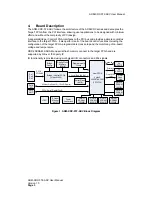
The ADM-XRC-5T2-ADV follows the architecture of the ADM-XRC series and decouples the
“target” FPGA from the PCI interface, allowing user applications to be designed with minimum
effort and without the complexity of PCI design.
A separate Bridge / Control FPGA interfaces to the PCI bus and provides a simple Local Bus
interface to the target FPGA. It also performs all of the board control functions including the
configuration of the target FPGA, programmable clock setup and the monitoring of on-board
voltage and temperature.
DDR2 SDRAM, SSRAM and serial flash memory connect to the target FPGA and are
supported by Xilinx or third party IP.
IO functionality is provided using multi-gigabit I/O connectors and Pn4 signals.
Bridge / Control FPGA
(Virtex4 LX25)
Config Flash
Memory
(32MB)
User FPGA
Virtex5
LX220T/LX330T
(FFG1738)
System
Monitor
(LM87)
Power
Conversion
Dual
Lane
Link
Local Bus (64 bit)
PCI-X /
PCI64/66
Bridge
Config
Serial Flash
(4MB)
Programmable
Clocks
DDR-II
SDRAM
(256MB)
Pn1
Pn2
Pn3
JTAG
Pn15
XMC
PCIe / Serial RapidIO (x8)
Front MGT
(x8)
DDR-II
SSRAM
(4MB)
2 x
ADV212
2 x
ADV212
DDR-II
SDRAM
(256MB)
DDR-II
SDRAM
(256MB)
DDR-II
SDRAM
(256MB)
DDR-II
SSRAM
(4MB)
Primary
Secondary
Pn14
I/O
32 User Defined I/O (16 LVDS pairs)
Figure 1 ADM-XRC-5T2-ADV Block Diagram
Version 1.0
Page 3


