background image

2

Introduction

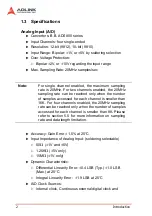
1.3 Specifications

Analog Input (A/D)

X

Converters: B.B. ADS800 series

X

Input Channels: four single-ended

X

Resolution: 12-bit (9812), 10-bit (9810)

X

Input Range: Bipolar: 

±

1V, or 

±

5V by soldering selection

X

Over Voltage Protection: 

Z

Bipolar 

±

2V, or 

±

10V regarding the input range

X

Max. Sampling Rate: 20MHz samples/sec

X

Accuracy: Gain Error 

±

1.5% at 25

°

C

X

Input Impedance of Analog Input: (soldering selectable)

Z

50

  (

±

1V and 

±

5V)

Z

1.25K

 (

±

5V only)

Z

15M

 (

±

1V only)

X

Dynamic Characteristic:

Z

Differential Linearity Error: 

±

0.4 LSB (Typ.) 

±

1.0 LSB 

(Max.) at 25

°

C

Z

Integral Linearity Error:  

±

1.9 LSB at 25

°

C

X

A/D Clock Sources:

Z

Internal clock, Continuous external digital clock and 

Note:

For single channel enabled, the maximum sampling
rate is 20MHz. For two channels enabled, the 20MHz
sampling rate can be reached only when the number
of samples accessed for each channel is smaller than
16K. For four channels enabled, the 20MHz sampling
rate can be reached only when the number of samples
accessed for each channel is smaller than 8K. Please
refer to section 5.5 for more information on sampling
rate and data length limitation.

Содержание NuDAQ PCI-9810

Страница 1: ...Advance Technologies Automate the World Manual Rev 3 00 Revision Date March 10 2005 Part No 51 11116 202 NuDAQ PCI 9812 10 20MHz Simultaneous 4 CH Analog Input Card User s Manual ...

Страница 2: ...ility to use the product or documentation even if advised of the possibility of such damages This document contains proprietary information protected by copyright All rights are reserved No part of this manual may be reproduced by any mechanical electronic or other means in any form without prior written permission of the manufacturer Trademarks NuDAQ PCI 9812 DAQBench PCIS DASK are registered tra...

Страница 3: ...vice adlinktech com TEL 886 2 82265877 FAX 886 2 82265717 Address 9F No 166 Jian Yi Road Chungho City Taipei 235 Taiwan Please email or FAX this completed service form for prompt and satisfactory service Company Information Company Organization Contact Person E mail Address Address Country TEL FAX Web Site Product Information Product Model Environment OS M B CPU Chipset BIOS Please give a detailed...

Страница 4: ......

Страница 5: ...EE HP VEE Driver 5 DAQBenchTM ActiveX Controls 5 DASYLabTM PRO 6 2 Installation 7 2 1 Checklist 7 2 2 Unpacking 8 2 3 PCI 9812 10 s Layout 9 2 4 Hardware Installation Outline 10 PCI configuration 10 PCI slot selection 10 Installation Instructions 10 2 5 Device Installation for Windows Systems 11 3 Signal Connection 13 3 1 Connectors 13 3 2 Analog Input Impedance Setting 15 Analog Input 15 External...

Страница 6: ...rsion Procedure 31 5 2 A D Signal Source Control 32 5 3 A D Trigger Source Control 32 Trigger Sources 33 Simultaneous Trigger for Multiple Cards 34 Trigger Modes 35 5 4 A D Clock Source Control 37 A D Clock Sources 37 Internal Pacer Clock 37 External Pacer Clock 38 Multiple Cards Operation 38 5 5 A D Data Transfer 39 AD Data Transfer 39 Simultaneous Sampling of four AD Channels 39 Total Data Throu...

Страница 7: ...0 _9812_Set_Trig 56 6 11 W_9812_Alloc_DMA_Mem 58 6 12 W_9812_Free_DMA_Mem 59 6 13 W_9812_Get_Sample 60 7 Calibration 61 7 1 What you need 61 7 2 VR Assignment 61 7 3 A D Calibration 62 AD Calibration for Channel 0 62 AD Calibration for Channels 1 2 3 62 8 Software Utility 63 8 1 Running 9812util exe 63 8 2 System Configuration 64 8 3 Calibration 64 8 4 Functional Testing 66 Warranty Policy 69 ...

Страница 8: ...ype connector 14 Table 3 3 Analog Input 15 Table 3 4 Switches and Resistors 17 Table 4 1 I O Address 19 Table 4 2 Five Trigger Modes 22 Table 4 3 Relationship between 8 bit trigger level and trigger voltage 23 Table 6 1 Data Types 46 Table 7 1 Functions of VRs 61 Table 7 2 AD Calibration for Channels 1 2 3 62 ...

Страница 9: ... of the PCI 9812 10 9 Figure 3 1 Location of connectors 13 Figure 5 1 Post Trigger Acquisition 35 Figure 5 2 Pre Trigger Acquisition 36 Figure 5 3 Middle Trigger Acquisition 36 Figure 5 4 Delay Trigger Acquisition 37 Figure 5 5 Block Diagram of PCI 9812 39 ...

Страница 10: ...vi ...

Страница 11: ...tions 1 1 Features PCI 9812 PCI Bus Advanced Data Acquisition Card is designed with the following advanced features X 32 bit PCI Bus Bus Mastering DMA data transfer X 12 bit 9812 or 10 bit 9810 analog input resolution X Onboard 32K words samples A D FIFO memory X Up to 20MHz A D sampling rate X Four single ended analog input channels X Bipolar input signals X Four A D converters simultaneously sam...

Страница 12: ...nly X Dynamic Characteristic Z Differential Linearity Error 0 4 LSB Typ 1 0 LSB Max at 25 C Z Integral Linearity Error 1 9 LSB at 25 C X A D Clock Sources Z Internal clock Continuous external digital clock and Note For single channel enabled the maximum sampling rate is 20MHz For two channels enabled the 20MHz sampling rate can be reached only when the number of samples accessed for each channel i...

Страница 13: ...trigger X AD Data Transfer Method DMA Bus mastering Digital Input X Number of channels Z Three TTL compatible inputs with 10KΩ pull down resistor X Input Voltage Z Low Min 0V Max 0 8V Z High Min 2 0V Max 5 5V Input Load Z Low 1uA 0V Z 0 5mA 5V Z High 2 7V min 20mA max General Specifications X Connectors 5 BNC type one 10 pin header X Operating Temperature 0 C to 40 C X Storage Temperature 20 C to ...

Страница 14: ...l license Programming Library For customers writing their own programs we provide function libraries for many different operating systems including DOS Library Borland C C and Microsoft C the functions descriptions are included in this user s guide Windows 95 DLL For VB VC Delphi and BC5 the functions descriptions are included in this user s guide PCIS DASK Include device drivers and DLL for Windo...

Страница 15: ...oard These can be installed and used without a license For more information on PCIS LVIEW please refer to the user s guide in the CD Manual_PDF Software PCIS LVIEW PCIS VEE HP VEE Driver The PCIS VEE includes user objects which are used to interface with HP VEE software package PCIS VEE supports Windows 95 98 NT The HP VEE drivers are free shipped with the board These can be installed and used wit...

Страница 16: ...ion DASYLabTM PRO DASYLab is an easy to use software package providing easy setup instrument functions such as FFT analysis Please contact ADLINK for DASYLab PRO which includes DASYLab and ADLINK hardware drivers ...

Страница 17: ... using only the software package when your system is running Please follow the steps below to install the PCI 9812 10 products X Go through the checklist section 2 1 X Unpacking section 2 2 X Check the PCB section 2 3 X Install the hardware section 2 4 2 1 Checklist In addition to this User s Guide the package includes the following items X PCI 9812 10 Enhanced Multi function Data Acquisition Card...

Страница 18: ...s Shipping and handling may cause damage to your module Be sure there are no shipping and handling damages on the modules carton before continuing After opening the card module carton extract the system module and place it only on a grounded anti static surface with component side up Again inspect the module for damages Press down on all the socketed IC s to make sure they are properly seated Do t...

Страница 19: ...Installation 9 2 3 PCI 9812 10 s Layout Figure 2 1 PCB Layout of the PCI 9812 10 ...

Страница 20: ...methods PCI slot selection The PCI card can be inserted to any PCI slot without any configuration for system resource Please note that the PCI system board and slot must provide bus mastering capability to operate this board well Installation Instructions 1 Turn off your computer 2 Turn off all accessories printer modem monitor etc connected to your computer 3 Remove the cover from your computer 4...

Страница 21: ...lug and Play function of Windows system will find the new NuDAQ NuIPC cards If this is the first time installing NuDAQ NuIPC cards in your Windows system you will be informed to enter the device information source Please refer to the Software Installation Guide for instructions on installing the device ...

Страница 22: ...12 ...

Страница 23: ...I 9812 10 connects to external devices through five BNC connectors and one 10 pin dual in line header Figure 3 1 shows the location of these connectors Figure 3 1 Location of connectors J1 The J1 BNC connector is used for the input signal of channel 0 A D converter J2 The J2 BNC connector is used for the input signal of channel 1 A D converter J3 The J3 BNC connector is used for the input signal o...

Страница 24: ...in D type connector through a ribbon cable the pin out of the D type connector is changed to Table 3 2 Pin out of JP1 connected to 9 pin D type connector Signal Pin Pin Signal External Clock Input 1 1 6 Ground Ground 2 7 Digital Input 1 External Digital Trigger Input 3 8 Ground Ground 4 9 Digital Input 2 Digital Input 0 5 10 Ground Table 3 1 Pin out of JP1 Signal Pin Pin Signal External Clock Inpu...

Страница 25: ...yout A solder gap switch consists of two copper pads the switch can be turned on by soldering these two pads together As all four channels use the same method to configure their input characteristics only channel 0 is discussed here There are two solder gap switches named C0LO channel 0 low impedance and C05V channel 0 5V input to setup the input characteristics of channel 0 Please refer to figure...

Страница 26: ...to saturation in the output stage Although a current limiting resistor is used to protect the ADC the large current brought by the saturation would damage the ADC 2 Offset problems will result if one uses high impedance 15MOhms with signal sources having high output impedance The high output impedance and the input bias current of up to 35uA introduces a voltage drop ranging several volts Adjustin...

Страница 27: ...to a digital clock with a long rise time When the rise time of a clock signal is too long the CPLD may work unpredictably meanwhile the real sample clock fed into the ADC will not be continuous explaining why users would see the strange sampled waveform when using a slower sine wave clock If slower sampling rate is necessary when using PCI 9812 10 users could feed a sine wave clock that has the fr...

Страница 28: ...ction Digital Input PCI 9812 10 has four digital inputs one external digital trigger JP1 pin3 and three general purpose digital inputs JP1 pin5 7 and 9 These inputs are TTL compatible with 10K ohm pull down resistors ...

Страница 29: ...emory space by using 32 bit data therefore both data read and write will be based on 32 bit data transfer Table 4 1 lists the I O address of each register with respect to the base address as well as the function of each register I O Address Read Write Base 0 ADC Channel Enable Reg Base 4 ADC Clock Divisor Reg Base 8 Trigger Mode Reg Base C Trigger Level Reg Base 10 Trigger Source Reg Base 14 Post ...

Страница 30: ...nable register Address BASE 0 Attribute write only Data Format Bit 31 4 any value Bit 3 CH3EN Bit 2 CH2EN Bit 1 CH1EN Bit 0 CH0EN Legal combinations refer to section 5 5 of these four bits are 0000 no channel is enabled 0001 only CH0 is enabled 0011 CH0 and CH1 are enabled 1111 all channels are enabled Bit 7 6 5 4 3 2 1 0 BASE 0 CH3EN CH2EN CH1EN CH0EN BASE 1 BASE 2 BASE 3 ...

Страница 31: ...k The frequency of the ADC sampling clock is Frequency of source clock ADC clock divisor Address BASE 04h Attribute write only Data Format DIV15 0 The AD clock frequency devisor Any value Bit 7 6 5 4 3 2 1 0 Base 4 DIV7 DIV6 DIV5 DIV4 DIV3 DIV2 DIV1 DIV0 Base 5 DIV15 DIV14 DIV13 DIV12 DIV11 DIV10 DIV9 DIV8 Base 6 Base 7 Note The minimum value of this register is 2 and the DIV0 is hardwired to 0 ...

Страница 32: ... Address BASE 08h Attribute write only Data Format TRGMOD2 0 Trigger mode Any value Bit 7 6 5 4 3 2 1 0 Base 8 TRGMOD2 TRGMOD1 TRGMOD0 Base 9 Base A Base B TRGMOD2 TRGMOD1 TRGMOD0 Trigger Mode 0 0 0 Software trigger 0 0 1 Post trigger 0 1 0 Pre trigger 0 1 1 Delay trigger 1 0 0 Middle trigger Table 4 2 Five Trigger Modes Note All other values of this register are illegal and PCI 9812 10 will not a...

Страница 33: ...ata Format TRGLVL7 0 trigger level Any value Relationship between the 8 bit trigger level and the trigger voltage Bit 7 6 5 4 3 2 1 0 BASE Ch TRGLVL7 TRGLVL6 TRGLVL5 TRGLVL4 TRGLVL3 TRGLVL2 TRGLVL1 TRGLVL0 BASE Dh BASE Eh BASE Fh TRGLVL7 0 bit 7 0 Trigger voltage 1V Trigger voltage 5V 0xFF 0 992V 4 96V 0xFE 0 984V 4 92V 0x81 0 008V 0 04V 0x80 0 000V 0 00V 0x7F 0 008V 0 04V 0x01 0 992V 4 96V 0x00 1...

Страница 34: ... trigger TRGSRC2 TRGSRC0 trigger source When the external digital trigger is selected the positive slope trigger equals to rising edge trigger the negative slope trigger equals to falling edge trigger and the value of trigger level register is meaningless Bit 7 6 5 4 3 2 1 0 Base 10 TRGSLP TRGSRC2 TRGSRC1 TRGSRC0 Base 11 Base 12 Base 13 TRIGSRC2 TRIGSRC2 TRIGSRC2 trigger source 0 0 0 CH0 0 0 1 CH1...

Страница 35: ...counter stops The counter is used to control the delay time in delay trigger mode and to control the post trigger sampling count in middle trigger mode Address BASE 14h Attribute write only Data Format PSTCNT15 0 This value is pre loaded to the post trigger counter when the post trigger counter register is written Any value Bit 7 6 5 4 3 2 1 0 BASE Ch PSTCN 7 PSTCN 6 PSTCN 5 PSTCN 4 PSTCN 3 PSTCN ...

Страница 36: ...The FIFO is not half full yet 1 The FIFO is at least half full Bit 2 FIFOOR FIFO output ready flag 0 The FIFO is not ready for output indicating FIFO is empty 1 The FIFO is ready for output not empty Bit 3 PTC0 post trigger counter is 0 0 The post trigger counter is not 0 1 The post trigger counter reaches 0 Bit 4 TD trigger detection flag 0 The trigger condition is not met yet no trigger is detec...

Страница 37: ...gister This register is used to control the onboard FIFO memory Address BASE 18h Attribute write Data Format Bit 0 CLRFIFO clear the onboard FIFO When a 1 is written to this bit the entire onboard FIFO is cleared Bit 1 CLRTRG clear trigger detection flag When a 1 is written to this bit the trigger detection bit is cleared Bit 2 31 Any value Bit 7 6 5 4 3 2 1 0 BASE 18h CLRTRG CLRFIFO BASE 19h BASE...

Страница 38: ...812 10 is ready to sample data When a 0 is written the PCI 9812 10 is disabled 4 11 Clock Source Register The register is used to select the system clock source Address BASE 20h Attribute write only Data Format Bit 31 3 Any value Bit 2 1 CLKSRC1 0 ADC clock source Bit 0 Freq_Sel Frequency selection Bit 7 6 5 4 3 2 1 0 BASE 18h ACQEN BASE 19h BASE 1Ah BASE 1Bh Bit 7 6 5 4 3 2 1 0 BASE 18h CLKSRC1 C...

Страница 39: ...are not required to write any hardware dependent low level programs to operate PCI 9812 10 Because it is more complex to control the PCI controller and the information is not described in this manual ADLINK does not recommend its users to program its applications based on low level programming The PCI controller used in the PCI 9812 is AMCC S5933 For further information on the s5933 PCI controller...

Страница 40: ...30 ...

Страница 41: ...Users can decide which channels to use and connect the signals to PCI 9812 10 In addition users should define and control the A D signal sources including the A D channels A D gains and A D signal types Please refer to section 5 2 for A D signal source control After deciding the A D signal source users must decide how to trigger the A D conversion and define control the trigger source The A D conv...

Страница 42: ...e channel number Please refer to section 4 2 Signal Range and Input impedance The proper signal range is important for data acquisition The available signal input ranges for 9812 10 are 5V or 1V which are set by soldering the copper pads on the PCB The input impedance for high speed applications should also be considered The selectable input impedance values are 50 Ohm 1 25K 15M ohm Please refer t...

Страница 43: ...ftware trigger The trigger event occurs when you call _9812_AD_DMA_Start function to start the operation External Analog Trigger You can use the signal on any analog input channel CH0 CH1 CH2 or CH3 as the trigger signal for external analog trigger The trigger conditions for analog triggers are described as follows Positive slope trigger The trigger event occurs the first time the trigger signal a...

Страница 44: ...r for Multiple Cards When multiple PCI 9812 cards are used in one system the trigger sources of every card can be connected together to provide the function of simultaneous trigger for multiple cards Please note that simultaneous trigger is not equivalent to simultaneous A D conversion The theoretical time difference between the samples on different card will be of the clock period Refer to sectio...

Страница 45: ...ger Acquisition Pre Trigger Acquisition Use pre trigger acquisition to collect data before a specified trigger event The trigger can either be an external analog trigger or digital trigger The data acquisition starts when DMA operation starts The operation stops when the external trigger event occurs If the external trigger occurs before the specified count of data is read specified by the _9812_A...

Страница 46: ...sired number of samples after trigger event is pre loaded in post trigger counter register and will count down on the rising edge of ADC sampling clock after the trigger condition is met When the count reaches 0 the counter stops The trigger can either be an external analog trigger or digital trigger Delay Trigger Acquisition Use delay trigger acquisition to delay the data collection after the occ...

Страница 47: ...s are in a pipelined structure which require eight conversion clocks to complete the conversion of digital data A D Clock Sources The A D converters operate under the paced mode which uses pacer clock for A D conversion at a fixed rate PCI 9812 10 supports three clock sources for analog input conversion X Internal A D pacer clock default X External sine wave clock X External square clock These thr...

Страница 48: ...ling frequency The formula is shown below Sampling Rate Frequency of Source Clock ADC Clock Divisor Multiple Cards Operation When multiple cards are used in one system 4 channels on one card can achieve simultaneous conversion because of the same internal clock source However the channels between two cards cannot be synchronized because the clock sources on different cards come from different sour...

Страница 49: ...ations due to the high total data throughput Users should refer to the following block diagram to understand how the analog signal is converted to digital form and transferred to PC host memory The data transfer rate limitation and the bottleneck will also be introduced in this section Figure 5 5 Block Diagram of PCI 9812 Simultaneous Sampling of four AD Channels The PCI 9812 10 is equipped with f...

Страница 50: ...Therefore two 16K words samples FIFO are designed for buffering the data There is a total of 32K word 32K samples when FIFO is onboard When four channels are used the FIFO size is 8K samples per channel When only two channels 0 and 1 are used the FIFO size is 16K samples per channel When only channel 0 is used the FIFO size is 32K samples Users would need to calculate the total data throughput for...

Страница 51: ...that even when the acquiring data length is less than the FIFO the AD data will not be kept in the FIFO but will be directly transferred to host memory by bus mastering DMA The DMA transfer mode is very complex to program ADLINK recommends using a high level program library to manipulate this card If the user wishes to program the software that can handle the DMA bus master data transfer please re...

Страница 52: ... to allocate a large memory size by keeping the memory clean The PCI bus mastering DMA controller of PCI 9812 needs continuous memory to store the AD data Summary So far the AD data transferring the maximum sampling rate and the maximum continuous data length at the sample time have been discussed Below is a summary of the steps discused 1 Calculate the total data throughput 2 Check if the total d...

Страница 53: ...y software The relationship between the real signal voltage and the sampled value is shown in the following table A D Data Hex Decimal Value V Volts 1V to 1V V Volts 5V to 5V 7FF 0 32752 1 0000 5 0000 400 0 16384 0 5002 2 5010 001 0 16 0 0005 0 0025 000 0 0 0 0000 0 0000 FFF 0 16 0 0005 0 0025 C00 0 16384 0 5002 2 5010 801 0 32752 1 0000 5 0000 800 0 32768 1 0049 5 0024 A D Data Hex Decimal Value ...

Страница 54: ...ween the A D data and the analog value is Voltage AD_data x 1 K x Gain Where Gain and K are constants For analog input range 1V to 1V Gain 1 For analog input range 5V to 5V Gain 5 For PCI 9812 K 2047x16 32752 For PCI 9810 K 511x64 32704 ...

Страница 55: ... allows calls to a DLL It provides the C C VB and Delphi include files 6 1 Libraries Installation Please refer to the Software Installation Guide for further information on the installation of software libraries for DOS Windows 95 DLL or PCIS DASK for Windows 98 NT 2000 The device drivers and DLL functions of Windows 98 NT 2000 are included in the PCIS DASK Please refer to the PCIS DASK user s gui...

Страница 56: ... used in your application programs The following table lists the data type names and their range Type Name Description Range U8 8 bit ASCII character 0 to 255 I16 16 bit signed integer 32768 to 32767 U16 16 bit unsigned integer 0 to 65535 I32 32 bit signed integer 2147483648 to 2147483647 U32 32 bit single precision floating point 0 to 4294967295 F32 32 bit single precision floating point 3 402823...

Страница 57: ..._no U16 pci_master Visual Basic Windows 95 W_9812_Initial ByVal card_number As Long op_base_address As Integer pt_base_address As Integer irq_no As Integer pci_master As Integer As Long Argument card_number The card number of PCI 9812 10 to be initialized There are 10 cards with valid card numbers ranging from 0 to 9 op_base_address The physical location of S5933 operation registers in I O space p...

Страница 58: ...ion This function is used to close a previously initialized 9812 card Syntax C C DOS int _9812_Close int card_number C C Windows 95 int W_9812_Close int card_number Visual Basic Windows 95 W_9812_Close ByVal card_number As Long As Long Argument card_number The card number of PCI 9812 to be closed the valid card numbers are 0 to 9 Return Code PCICardNumErr PCICardNotInit NoError ...

Страница 59: ...ntax C C DOS int _9812_AD_DMA_Start int card_number int ch_cnt U32 buff U32 count C C Windows 95 int W_9812_AD_DMA_Start int card_number int ch_cnt HANDLE memID U32 count Visual Basic Windows 95 W_9812_AD_DMA_Start ByVal card_number As Long ByVal ch_cnt As Long ByVal handle As Long ByVal count As Long As Long Argument card_number The card number of PCI 9812 ch_cnt Number of A D channel enabled The...

Страница 60: ... data 9810 b2 b1 b0 digital input data from channel DI2 DI1 DI0 b3 trigger detection flag 0 no trigger is detected 1 trigger is detected memID Win 95 The memory ID of the allocated system DMA memory In Windows 95 environment before calling W_9812_AD_DMA_Start W_9812_Alloc_DMA_Mem must be called to allocate a contiguous DMA memory W_9812_Alloc_DMA_Mem will return a memory ID for identifying the all...

Страница 61: ...heck its operation status Syntax C C DOS int _9812_AD_DMA_Status int card_number int count int status U32 start_idx C C Windows 95 int W_9812_AD_DMA_Status int card_number int count int status U32 start_idx Visual Basic Windows 95 W_9812_AD_DMA_Status ByVal card_number As Long count As Long status As Long start_idx As Long As Long Argument card_number The card number of PCI 9812 10 to be selected ...

Страница 62: ..._trig 3 DMA_wait_delay start_idx The index where the data starts from is in the user s buffer i e the sequence of read data is buff start_idx buff start_idx 1 _ buff 0 buff 1 _ buff start_idx 1 Return Code PCICardNumErr PCICardNotInit NoError ...

Страница 63: ...ta transfer is stopped by this function or by the DMA terminal count ISR Syntax C C DOS int _9812_AD_DMA_Stop int card_number U32 count C C Windows 95 int W_9812_AD_DMA_Stop int card_number U32 count Visual Basic Windows 95 W_9812_AD_DMA_Stop ByVal card_number As Long count As Long As Long Argument card_number The card number of PCI 9812 to be selected count The amount of A D data that has been tr...

Страница 64: ...t_Clk_Src ByVal card_number As Long ByVal clk_src As Long ByVal ftpci As Long As Long Argument card_number The card number of PCI 9812 10 to be selected clk_src The ADC clock source the valid values are as follows 0 INT_CLK internal clock 1 SIN_CLK external sin wave clock 2 SQR_CLK external square clock ftpci Frequency selection AD2_GT_PCI The frequency of A D clock source is higher than PCI clock...

Страница 65: ...4 Syntax C C DOS int _9812_Set_Clk_Rate int card_number U16 clk_div C C Windows 95 int W_9812_Set_Clk_Rate int card_number U16 clk_div Visual Basic Windows 95 W_9812_Set_Clk_Rate ByVal card_number As Long ByVal clk_div As Integer As Long Argument card_number The card number of PCI 9812 to be selected clk_div The ADC clock divisor this value must be an even number and the minimum value is 2 Return ...

Страница 66: ...U16 post_trig_cnt C C Windows 95 int W_9812_Set_Trig int card_number int trig_mode int trig_src int trig_pol int trig_lvl U16 post_trig_cnt Visual Basic Windows 95 W_9812_Set_Trig ByVal card_number As Long ByVal trig_mode As Long ByVal trig_src As Long ByVal trig_pol As Long ByVal trig_lvl As Long ByVal post_trig_cnt As Integer As Long Argument card_number The card number of PCI 9812 to be selecte...

Страница 67: ... level and the trigger voltage is shown in section 4 5 post_trig_cnt Post trigger count This value is preloaded to the post trigger counter when the post trigger counter register is written It will count down on the rising edge of ADC sampling clock after the trigger condition is met When the count reaches 0 the counter stops The counter is used to control the delay time in delay trigger mode and ...

Страница 68: ...W_9812_Alloc_DMA_Mem ByVal buf_size As Long memID As Long linearAddr As Long As Long Argument buf_size Bytes to allocate note that the unit of this argument is BYTE not SAMPLE memID If the memory allocation is successful driver returns the ID of that memory in this argument Use this memory ID in W_9812_AD_DMA_Start function call linearAddr The linear address of the allocated DMA memory This linear...

Страница 69: ... Windows 95 environment This function is only available in Windows 95 Syntax C C Windows 95 int W_9812_Free_DMA_Mem HANDLE memID Visual Basic Windows 95 W_9812_Free_DMA_Mem ByVal memID As Long As Long Argument memID The memory ID of the system DMA memory to deallocate Return Code NoError ...

Страница 70: ...ailable in Windows 95 Syntax C C Windows 95 int W_9812_Get_Sample U32 linearAddr U32 index I16 ai_data Visual Basic Windows 95 W_9812_Get_Sample ByVal linearAddr As Long ByVal idx As Long ai_data As Integer As Long Argument linearAddr The linear address of the allocated DMA memory index The index of the sample The first sample is with index 0 ai_data Returns the samples retrieved Return Code NoErr...

Страница 71: ...process once executed This program is included in the delivered package X A voltage calibrator or a very stable and noise free DC voltage generator 7 2 VR Assignment There are eight variable resistors VR on the PCI 9812 10 board that allows the user to make accurate adjustments on A D channels The function of each VR is specified in Table 7 1 VR1 A D channel 0 offset adjustment VR2 A D channel 1 o...

Страница 72: ...hown in section 7 3 by trimming the corresponding VRs Please refer to the following table when calibrating other channels A calibration utility is provided in the software CD which is included in the package Details of the calibration procedures and description can be found in this utility Simply follow the instructions in the software calibration utility The measurement data can also be found wit...

Страница 73: ...erating guidance but also graphics to instruct the user on setting the hardware configuration correctly This utility is described in the sections below 8 1 Running 9812util exe After finishing the DOS installation the utility can be executed by typing the following assuming your utility is located in ADLINK DOS 9812 Util directory C cd ADLINK DOS 9812 Util C 9812UTIL The following diagram will be ...

Страница 74: ...ation process of PCI 9812 10 The calibration program serves as a useful test for the PCI 9812 10 s A D D A and DIO functions and can be a useful tool when troubleshooting problems When choosing the calibration function from the main menu list the calibration item menu is displayed on the screen After Note For an environment with frequent large fluctuations in temperature and vibration a recalibrat...

Страница 75: ...indow shows the step by step calibration instructions The lower window shows the layout of PCI 9812 10 In addition the proper Variable Resister VR will blink to indicate the related VR needs to be adjusted for the current calibration step For example if you select 3 the following window will be displayed on the screen ...

Страница 76: ...l Testing This function is used to test the functions of PCI 9812 10 A D When choosing a testing function from the main menu list a function testing test window is displayed on the screen The following is an example of a testing window ...

Страница 77: ...er finishing adjusting these settings press Enter to start performing the test function With this function you can test and view the different effect of various trigger modes In addition an arrow shown on the screen indicates the trigger position If the trigger source is also an enabled A D channel you can easily view the result of changing trigger levels The following diagram is a snapshot of the...

Страница 78: ...68 Software Utility ...

Страница 79: ...manufactured by ADLINK will be covered by the original manufacturers warranty X For products containing storage devices hard drives flash cards etc please back up your data before sending them for repair ADLINK is not responsible for loss of data X Please ensure the use of properly licensed software with our systems ADLINK does not condone the use of pirated software and will not service systems u...

Страница 80: ...icals X Damage caused by leakage of battery fluid during or after change of batteries by customer user X Damage from improper repair by unauthorized technicians X Products with altered and or damaged serial numbers are not entitled to our service X Other categories not protected under our warranty 4 Customers are responsible for shipping costs to transport damaged products to our company or sales ...

Отзывы: