background image

SERIES AP470 ACROPACK  

USER

’S MANUAL 


Acromag, Inc. Tel: 248-295-0310  

            - 34 -                                   

http://www.acromag.com  

- 34 - 

www.acromag.com 


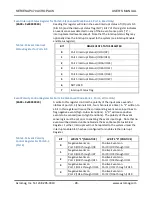
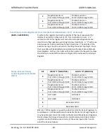
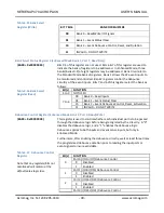
XADC Status/Control Register (Accessible in Standard and Enhanced Mode) (Read/Write)  

(BAR0 + 0x0000 0048)   

This read/write register will access the XADC register at the address set in 
the XADC Address Register. This allows the board’s temperature and supply 
voltages to be read. 

For example, the address of the XADC Status register that is to be accessed 
is first set via the XADC Address register at BAR0 plus 0x4CH.  Next, this 
register at BAR0 plus 0x48H is read.  Bits 22 to 16 of this register hold the 
address of the XADC register that is accessed.  Data bits 15 to 6 of this 
register hold the “ADCcode” temperature, Vccint, or Vccaux value.  Data bits 
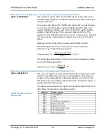
5 to 0 are not used.  Valid addresses are given in column one of the table 
below. 

Reading or writing this register is possible via 32-bit data transfers. 

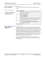
The 10-bits digitized and output from the ADC can be converted to 
temperature by using the following equation. 

15

.

273

1024

975

.

503

)

(

ADCcode

C

e

Temperatur


The 10-bits digitized and output from the ADC can be converted to voltage 
by using the following equation. 

V

ADCcode

volts

age

SupplyVolt

3

1024

)

(


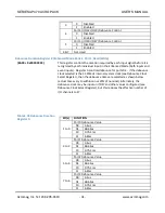
XADC Address Register (Accessible in Standard and Enhanced Mode) (Write Only)  

(Bar0 + 0x0000 004C)   


This write only register is used to set the XADC address register with a valid 
address for the XADC internal status or control registers.  Valid addresses 
are given in the following table.  Additional addresses can be found in the 
Xilinx XADC document UG480 (available from Xilinx).  Writing this register is 
possible via 32-bit data transfers. 

The address value written to this register can be read on bits 22 to 16 of the 
XADC Status/Control register at BAR0 plus 0x48H. 

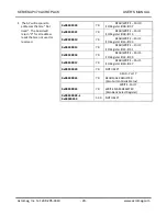
Table 3.20: System Monitor 
Register Map 


Address 

Status Register 

0x00 

Temperature 

0x01 

Vccint 

0x02 

Vccaux 

0x20 

Maximum Temperature 

0x21 

Maximum Vccint 

0x22 

Maximum Vccaux 

0x24 

Minimum Temperature 

0x25 

Minimum Vccint 

0x26 

Minimum Vccaux 


Содержание AcroPack AP470 Series

Страница 1: ...O Module USER S MANUAL ACROMAG INCORPORATED 30765 South Wixom Road Wixom MI 48393 2417 U S A Tel 248 295 0310 Fax 248 624 9234 Copyright 2016 Acromag Inc Printed in the USA Data and specifications are...

Страница 2: ...rmation 6 1 3 2 Key Features 6 1 3 3 Key Features PCIe Interface 7 1 4 Signal Interface Products 7 1 5 Software Support 8 Windows 8 VxWorks 8 Linux 8 1 6 References 8 2 0 PREPARATION FOR USE 9 2 1 Unp...

Страница 3: ...s 0 5 28 Event Polarity Control Register For Ports 0 3 Enhanced Mode Bank 1 Port 6 Write Only 28 Table 3 14 Event Polarity Control Register For Ports 0 3 Port 6 28 Event Polarity Control Register For...

Страница 4: ...4 1 Logic Power Interface 42 4 2 I O Ports 42 5 0 SERVICE AND REPAIR 43 5 1 Service and Repair Assistance 43 5 2 Preliminary Service Procedure 43 5 3 Where to Get Help 43 6 0 SPECIFICATIONS 44 6 1 Ph...

Страница 5: ...S MANUAL Acromag Inc Tel 248 295 0310 4 http www acromag com 4 www acromag com APPENDIX A 47 AP470 Functional Block Diagram 47 APPENDIX B 48 AP CC 01 Heatsink Kit Installation 48 CERTIFICATE OF VOLATI...

Страница 6: ...ep current the information contained in this manual No part of this manual may be copied or reproduced in any form without the prior written consent of Acromag 1 2 1 Trademark Trade Name and Copyright...

Страница 7: ...nd programmable debounce Interrupt event and debounce functionality applies to all 48 channels of this model The AP470 utilizes state of the art Surface Mounted Technology SMT to achieve its wide func...

Страница 8: ...ower up or power down for steady and safe control Open Drain Outputs Include Pull ups All outputs include 4 7K pull ups to 5V Overvoltage Protection Individual I O channels include over voltage clamps...

Страница 9: ...Acromag provides a software product sold separately consisting of VxWorks software This software Model APSW API VXW is composed of VxWorks real time operating system libraries for all AcroPack module...

Страница 10: ...oduct near strong electrostatic electromagnetic magnetic or radioactive fields unless the device is contained within its original manufacturer s packaging Be aware that failure to comply with these gu...

Страница 11: ...ovided to prevent a temperature rise above the maximum operating temperature 2 3 Non Isolation Considerations The board is non isolated since there is electrical continuity between the PCIe bus and Ac...

Страница 12: ...9 Field I O 6 12 Reserved isolation 11 Reserved isolation 4 4 7 14 Field I O 7 38 29 8 13 Field I O 8 16 Reserved isolation 15 Reserved isolation 5 5 9 18 Field I O 9 39 30 10 17 Field I O 10 20 Rese...

Страница 13: ...ed isolation 55 Reserved isolation 15 15 29 58 Field I O 29 49 40 30 57 Field I O 30 60 Reserved isolation 59 Reserved isolation 16 16 31 62 Field I O 31 50 41 32 61 Field I O 32 64 Reserved isolation...

Страница 14: ...I O 43 56 47 44 85 Field I O 44 88 Reserved isolation 87 Reserved isolation 23 23 45 90 Field I O 45 57 48 46 89 Field I O 46 92 Reserved isolation 91 Reserved isolation 24 24 47 94 Field I O 47 58 4...

Страница 15: ...e mating connector on the carrier board The pin assignments of this connector are standard for all AP modules according to the PCI Express MINI Card Electromechanical Specification REV 1 2 with except...

Страница 16: ...23 PERn0 24 3 3V3 21 GND 22 PERST 19 TDI UIM_C4 1 20 N C W_DISABLE 1 17 TDO UIM_C8 1 18 GND 15 GND 16 N C UIM_VPP 1 13 RECLK 14 N C UIM_RESET 1 11 REFCLK 12 N C UIM_CLK 1 9 GND 10 N C UIM_DATA 1 7 CLK...

Страница 17: ...ration registers A PCIe bus configuration access is used to access an AcroPack s configuration registers When the computer is first powered up the computer s system configuration software scans the PC...

Страница 18: ...ve on a board interrupt request Table 3 1 Configuration Registers Reg Num D31 D24 D23 D16 D15 D8 D7 D0 0 Device ID 0x7016 AP470 Vendor ID 16D5 1 Status Command 2 Class Code 118000 Rev ID 00 3 BIST Hea...

Страница 19: ...d Port 7 which is the Mask Register If the Enhanced Mode is selected then 3 additional banks of 8 registers are addressed to cover the additional functionality in this mode The first bank of the Enhan...

Страница 20: ...0000 0000 7 0 Interrupt Register 0x0000 0004 7 0 Location in System Register Table 3 2 Standard Mode Memory Map Notes 1 The AP470 will respond to addresses that are Not Used The board will return 0 fo...

Страница 21: ...x0000 000C 7 0 READ WRITE Port 1 I O Register IO08 IO15 0x0000 0010 7 0 READ WRITE Port 2 I O Register IO16 IO23 0x0000 0014 7 0 READ WRITE Port 3 I O Register IO24 IO31 0x0000 0018 7 0 READ WRITE Por...

Страница 22: ...lear Reg Port 1 I O points 8 15 0x0000 0010 7 0 READ Port 2 Event Sense Status Reg Port 2 I O points 16 23 0x0000 0010 7 0 WRITE Port 2 Event Sense Clear Reg Port 2 I O points 16 23 0x0000 0014 7 0 RE...

Страница 23: ...nd to addresses that are Not Used The board will return 0 for all address reads that are not used or reserved BAR0 Base Address Bit s Description 0x0000 0008 7 0 READ WRITE Port 0 Debounce Control Reg...

Страница 24: ...3 7 This register can be read or written with either 8 bit 16 bit or 32 bit data transfers A power up or system reset sets all interrupt register bits to 0 With both an enabled Event Sense bit and Boa...

Страница 25: ...arrier XXXXX System Slot identification bits are described by the AcroPack carrier card 31 to 8 Not Used Port Registers Standard Mode Ports 0 5 Read Write BAR0 0x0000 0008 0x0000 001C Six registers ar...

Страница 26: ...of operation To switch to Enhanced Mode four unique bytes must be written to port 7 in consecutive order without doing any reads or writes to any other port and with interrupts disabled The data patte...

Страница 27: ...ort 3 Write Mask Port 3 Write Mask 4 Port 4 Write Mask Port 4 Write Mask 5 Port 5 Write Mask Port 5 Write Mask 6 Bank Select Bit 0 Bank Status Bit 0 7 Bank Select Bit 1 Bank Status Bit 1 Bits 6 7 of t...

Страница 28: ...terrupt Enable bits are set then interrupts can be generated Changing Debounce control registers while interrupts are enabled can cause false interrupts It is recommended that interrupts be disabled p...

Страница 29: ...0020 A write to this register controls the polarity of the input sense event for nibbles of ports 0 3 channels 0 31 four channels at a time A 1 written to a bit in this register will cause the corres...

Страница 30: ...ed until enabled via the Event Sense Status Clear Register Further interrupts will not be reported to the system unless the Interrupt enable bit 0 has been configured for enable via the Interrupt Regi...

Страница 31: ...ter Read Bit s FUNCTION 5 to 0 NOT USED 7 to 6 00 Bank 0 Read Inputs 01 Bank 1 Event Status Clear 10 Bank 2 Event Debounce Control Reset Duration 11 INVALID DO NOT WRITE Debounce Control Register Enha...

Страница 32: ...ounce for ports 0 3 If the debounce clock selected is the 31 25MHz internal system clock see Debounce Clock Select Register then the debounce times are selected as shown below actual times vary to wit...

Страница 33: ...egister controls the duration required by each input signal before it is recognized by each individual input in the Enhanced Mode both inputs and event inputs Register 1 controls debounce for ports 4...

Страница 34: ...0 5 of this register are not used Bits 6 7 of this register are used to select the bank of registers to be addressed In Enhanced Mode three banks banks 0 1 2 of eight registers may be addressed Bank...

Страница 35: ...ers The 10 bits digitized and output from the ADC can be converted to temperature by using the following equation 15 273 1024 975 503 ADCcode C e Temperatur The 10 bits digitized and output from the A...

Страница 36: ...0 1 05 Vccaux 1 71 1 8 1 89 Temperature operating range 40C 50 60C 100C Firmware Revision Register Read Only BAR0 0x0000 0200 This is a read only register The ASCII code representing the current revi...

Страница 37: ...al ports may also be masked from writes to the port when the port is intended for input only to help prevent contention errors Each port I O line includes an integrated 4 7k pull up resistor to 5V For...

Страница 38: ...ve or low to high level transitions positive Set each half port nibble to the desired polarity and then enable each of the event inputs to be detected Optionally set the interrupt enable bit the Inter...

Страница 39: ...hannels Interrupts are only generated in the Enhanced Mode for event channels when enabled via the Event Sense Status Register Writing 0 to the corresponding event sense bit in the Event Sense Status...

Страница 40: ...point you are in Enhanced Mode bank 0 Port 7 is used to access register banks 1 2 2 Write 80H to the port 7 address to select register bank 2 where debounce will be configured for our port 0 input ch...

Страница 41: ...tatus Register for port 0 I O points at the port 0 address in this bank Note that writing a 1 to a bit position enables the event sense detector while writing a 0 clears the event sensed without enabl...

Страница 42: ...vent Sense Status Register must be written with a 1 to re enable event sensing for subsequent events but only after first writing 0 to the corresponding bit position to clear the event sense flip flop...

Страница 43: ...tion to each other As such care must be taken to avoid ground loops Ignoring this effect may cause operation errors and with extreme abuse possible circuit damage A Field Programmable Gate Array FPGA...

Страница 44: ...OFF BEFORE SERVICING BOARDS Before beginning repair be sure that all of the procedures in the Preparation for Use section have been followed Also refer to the documentation of your carrier board to v...

Страница 45: ...ations requiring operating temperatures of 70 C to 85 C will require purchase of AcroPack Heatsink Accessory AP CC 01 with a minimum airflow of 200LFM For temperature below 70 C the module will requir...

Страница 46: ...with IEC 60068 2 27 30G 11ms half sine 50G 3mS half sine 18 shocks at 6 orientations for both test levels 6 3 5 EMC Directives The AcroPack is designed to comply with EMC Directive 2004 108 EC Immuni...

Страница 47: ...t Capacitance 20pF Max 10pF Typical Input Leakage Current 10 A Typical 6 6 Digital Outputs Output Channel Configuration 48 open drain CMOS outputs For DC voltage applications only observe proper polar...

Страница 48: ...SERIES AP470 ACROPACK USER S MANUAL Acromag Inc Tel 248 295 0310 47 http www acromag com 47 www acromag com Appendix A AP470 Functional Block Diagram Figure 1 AP470 Block Diagram...

Страница 49: ...Tel 248 295 0310 48 http www acromag com 48 www acromag com Appendix B AP CC 01 Heatsink Kit Installation This example will show how to install the AP CC 01 Heatsink kit with an APCe7020 carrier AP CC...

Страница 50: ...K USER S MANUAL Acromag Inc Tel 248 295 0310 49 http www acromag com 49 www acromag com 1 Install two standoffs and secure with two screws 2 Install the AcroPack module 3 Install the Heatsink and secu...

Страница 51: ...S AP470 ACROPACK USER S MANUAL Acromag Inc Tel 248 295 0310 50 http www acromag com 50 www acromag com 4 AP CC 01 Installation is complete Note Make sure the thermal pad is making contact with the FPG...

Страница 52: ...Sanitize Power Down Type SRAM SDRAM etc Size User Modifiable Yes No Function Process to Sanitize Non Volatile Memory Does this product contain Non Volatile memory i e Memory of whose contents is reta...

Страница 53: ...ry The revision history for this document is summarized in the table below Release Date Version EGR DOC Description of Revision 30 MAR 2016 A MDW MDW Preliminary Document Publication 18 JUL 2016 A MDW...

Отзывы: