background image

Z8018x
Family MPU User Manual

58

UM005004-0918


MMU Common/Bank Area Register (CBAR)

MMU Common Base Register (CBR)

MMU Bank Base Register (BBR)

CBAR is used to define the logical memory organization, while CBR and 
BBR are used to relocate logical areas within the 1024KB physical 
address space. The resolution for both setting boundaries within the 
logical space and relocation within the physical space is 4KB.

The CA field of CBAR determines the start address of Common Area 1 
(Upper Common) and by default, the end address of the Bank Area. The 
BA field determines the start address of the Bank Area and by default, the 
end address of Common Area 0 (Lower Common).

The CA and BA fields of CBAR may be freely programmed subject only 
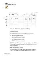
to the restriction that CA may never be less than BA. Figures 27 and 28 
illustrate examples of logical memory organizations associated with 
different values of CA and BA.

Figure 27. Logical Memory Organization

Common

Bank Area

Common

Common

Bank Area

Common

Common

Common

Common Area 1

Lower Limit Address

>

Bank Area

Lower Limit Address

>

0000H

Common Area 1

Lower lImit Address

>

Bank Area

Lower lImit Address

=

0000H

Common Area 1

Lower Limit Address

=

Bank Area

Lower Limit Address

>

0000H

Common Area 1

Lower Limit Address

=

Bank Area

Lower Limit Address

=

0000H

(RESET Condition)

Area 1

Area 1

Area 0

Area 1

Area 1

Area 0

Summary of Contents for Z8018 Series

Page 1: ...www zilog com Z8018x Family MPU User Manual UM005004 0918...

Page 2: ...gest possible uses and may be superseded ZiLOG INC DOES NOT ASSUME LIABILITY FOR OR PROVIDE A REPRESENTATION OF ACCURACY OF THE INFORMATION DEVICES OR TECHNOLOGY DESCRIBED IN THIS DOCUMENT ZiLOG ALSO...

Page 3: ...t of ZiLOG products that use this class of processor along with the associated processor family This document is also the core user manual for the following products Intended Audience This manual is w...

Page 4: ...eters and absolute maximum ratings for the Z8X180 MPUs AC Characteristics Presents the AC parameters for the Z8018x MPUs Timing Diagrams Contains timing diagrams and standard test conditions for the Z...

Page 5: ...ss Processors Only 31 Low Power Modes Z8S180 Z8L180 only 36 Add On Features 36 STANDBY Mode 37 STANDBY Mode Exit wiht BUS REQUEST 38 STANDBY Mode EXit with External Interrupts 39 IDLE Mode 40 STANDBY...

Page 6: ...156 Miscellaneous 172 Software Architecture 173 Instruction Set 173 CPU Registers 175 DC Characteristics 185 Absolute Maximum Rating 185 Z80180 DC Characteristics 186 Z8S180 DC Characteristics 187 Z8L...

Page 7: ...37 Op Code Map 247 Bus Control Signal Conditions 251 Bus and Control Signal Condition in each Machine Cycle 251 Interrupts 279 Operating Modes Summary 281 Request Acceptances in Each Operating Mode 28...

Page 8: ...Figure 9 Op Code Fetch without Wait State Timing Diagram 19 Figure 10 Op Code Fetch with Wait State Timing Diagram 20 Figure 11 Memory Read Write without Wait State Timing Diagram 21 Figure 12 Memory...

Page 9: ...re 33 TRAP Timing 3rd Op Code Undefined 72 Figure 34 NMI Use 74 Figure 35 NMI Timing 75 Figure 36 INT0 Mode 0 Timing Diagram 76 Figure 37 INT0 Mode 1 Interrupt Sequence 77 Figure 38 INT0 Mode 1 Timing...

Page 10: ...Figure 60 Transmit Timing External Clock 154 Figure 61 CSI O Receive Timing Internal Clock 155 Figure 62 CSI O Receive Timing External Clock 156 Figure 63 PRT Block Diagram 157 Figure 64 Timer Initia...

Page 11: ...82 AC Timing Diagram 2 198 Figure 83 CPU Timing IOC 0 I O Read Cycle I O Write Cycle 199 Figure 84 DMA Control Signals 200 Figure 85 E Clock Timing Memory R W Cycle I O R W Cycle 201 Figure 86 E Cloc...

Page 12: ...le 7 I O Address Map Z8S180 Z8L180 Class Processors Only 48 Table 8 State of IEF1 and IEF2 69 Table 9 Vector Table 82 Table 10 RETI Control Signal States 85 Table 11 DRAM Refresh Intervals 89 Table 12...

Page 13: ...86 Table 29 Z8S180 DC Characteristics 187 Table 30 Z8L180 DC Characteristics 189 AC Characteristics 193 Table 31 Z8S180 AC Characteristics 193 Instruction Set 207 Table 32 Register Values 207 Table 33...

Page 14: ...ruction Format CB XX 249 Table 50 2nd Op Code Map Instruction Format ED XX 250 Bus Control Signal Conditions 251 Table 51 Bus and Control Signal Condition in Each Machine Cycle 251 Table 52 Interrupts...

Page 15: ...O Port Code Compatible with ZiLOG Z80 CPU Extended Instructions GENERAL DESCRIPTION Based on a microcoded execution unit and an advanced CMOS manufacturing technology the Z80180 Z8S180 Z8L180 Z8X180 i...

Page 16: ...ion even further The SLEEP mode reduces power by placing the CPU into a stopped state thereby consuming less current while the on chip I O device is still operating The SYSTEM STOP mode places both th...

Page 17: ...13 A14 A15 A16 A17 A18 TOUT VCC 1 2 3 4 6 7 8 9 10 5 11 12 13 14 15 16 17 18 19 20 21 22 23 24 25 26 27 28 29 30 31 32 64 55 54 53 52 51 50 49 48 47 46 45 44 43 42 41 40 39 38 37 36 35 34 33 63 62 61...

Page 18: ...8 47 46 45 44 59 58 57 56 55 54 53 52 HALT TEND1 DREQ1 CKS RXS CTS1 TXS CKA1 TEND0 RXA1 TEST TXA1 CKA0 DREQ0 RXA0 TXA0 DCD0 CTS0 RTS0 D7 Z8X180 A12 A13 A14 9 68 67 66 65 64 63 62 61 8 7 6 5 4 3 2 1 NM...

Page 19: ...3 62 61 59 58 57 56 55 60 54 53 52 51 50 49 48 47 46 45 44 43 42 41 CKS RXS CTS1 TXS CKA1 TEND0 RXA1 TEST TXA1 NC CKA0 DREQ0 RXA0 TXA0 RFSH TEND1 DREQ1 DCD0 CTS RTS0 D7 NC NC D6 HALT NC NC A18 TOUT V...

Page 20: ...MACs 2 DREQ1 TEND1 CKA0 DREQ0 Interrupt Bus State Control Asynchronous SCI channel 1 RESET RD WR MI MREQ IORQ HALT WAIT BUSREQ BUSACK RFSH ST E NMI INT0 INT1 INT2 RXA0 RTS0 CTS0 DCD0 TXA0 TXA1 CKA1 TE...

Page 21: ...devices such as DMA controllers to request access to the system bus This request has a higher priority than NMI and is always recognized at the end of the current machine cycle This signal stops the...

Page 22: ...External Clock Crystal Input Active High Crystal oscillator connection An external clock can be input to the Z8X180 on this pin when a crystal is not used This input is Schmitt triggered HALT Halt Sl...

Page 23: ...and ST signal to decode status of the CPU machine cycle This signal is analogous to the LIR signal of the Z64180 MREQ Memory Request Output Active Low 3 state MREQ indicates that the address bus hold...

Page 24: ...and HALT output to decode the status of the CPU machine cycle Table 1 provides status summary TEND0 TEND1 Transfer End 0 and 1 Outputs Active Low This output is asserted active during the last write c...

Page 25: ...sed memory or I O devices are not ready for a data transfer This input is used to induce additional clock cycles into the current machine cycle The WAIT input is sampled on the falling edge of T2 and...

Page 26: ...criptions Multiplexed Pins Descriptions A18 TOUT During RESET this pin is initialized as A18 pin If either TOC1 or TOC0 bit of the Timer Control Register TCR is set to 1 TOUT function is selected If T...

Page 27: ...activity associated with both the CPU and some on chip peripherals This includes Wait State timing RESET cycles DRAM refresh and DMA bus exchanges Interrupt Controller This block monitors and priorit...

Page 28: ...block length up to 64KB and can cross over 64K boundaries Asynchronous Serial Communications Interface ASCI The ASCI logic provides two individual full duplex UARTs Each channel includes a programmab...

Page 29: ...RESET When M1E is 1 the M1 output is asserted Low during the Op Code fetch cycle the INT0 acknowledge cycle and the first machine cycle of the NMI acknowledge This action also causes the M1 signal to...

Page 30: ...e until the PIO sees an active M1 signal When M1TE is 1 there is no change in the operation of the M1 signal and M1E controls its function When M1TE is 0 the M1 output is asserted during the next Op C...

Page 31: ...0 family of peripherals The IORQ and RD signals go active as a result of the rising edge of T2 This timing allows the Z8X180 to satisfy the setup times required by the Z80 peripherals on those two sig...

Page 32: ...O or it consists of one system clock T1 during CPU internal operations The system clock is half the frequency of the Crystal oscillator that is an 8 MHz crystal produces 4 MHz or 250 nsec For interfa...

Page 33: ...ode fetch cycle Wait States TW are controlled by the external WAIT input combined with an on chip programmable Wait State generator At the falling edge of T2 the combined WAIT input is sampled If WAIT...

Page 34: ...latched at the falling edge of T3 Instruction operands include immediate data displacement and extended addresses and contain the same timing as memory data reads During memory write cycles the MREQ s...

Page 35: ...Figure 11 illustrates the read write timing without Wait States Tw while Figure 12 illustrates read write timing with Wait States TW Figure 11 Memory Read Write without Wait State Timing Diagram T1 T...

Page 36: ...Q I O Request signal is asserted Low instead of the MREQ signal The 16 bit I O address is not translated by the MMU A16 A19 are held Low At least one Wait State TW is always inserted for I O read and...

Page 37: ...ding Op Code fetch operand fetch and data read write cycles An instruction may also include cycles for internal processes which make the bus IDLE The example in Figure 14 illustrates the bus timing fo...

Page 38: ...begins with the two machine cycles to read the two byte instruction Op Code as indicated by M1 Low Next the instruction operand d is fetched Memory Write Cycle Next instruction Fetch Cycle CPU interna...

Page 39: ...control address and data bus ownership with another bus master The alternate bus master can request the bus release by asserting the BUSREQ Bus Request input Low After the Z8X180 releases the bus it...

Page 40: ...of time Figure 16 illustrates BUSREQ BUSACK bus exchange during a memory read cycle Figure 17 illustrates bus exchange when the bus release is requested during a Z8X180 CPU internal operation BUSREQ i...

Page 41: ...ed in both CPU execution and DMA transfer cycles When the external WAIT input is asserted Low Wait State s TW are inserted between T2 and T3 to extend the bus cycle duration The WAIT input is sampled...

Page 42: ...the WAIT input Wait States TW can also be inserted by program using the Z8X180 on chip Wait State generator see Figure 19 Wait State TW timing applies for both CPU execution and on chip DMAC cycles By...

Page 43: ...WI0 Memory Wait Insertion For CPU and DMAC cycles which access memory including memory mapped I O zero to three Wait States may be automatically inserted depending on the programmed value in MWI1 and...

Page 44: ...or NMI interrupt acknowledge cycles when M1 is Low Note 2 0 0 1 0 Note 1 2 2 0 0 1 2 4 1 0 3 5 1 1 4 6 Note 1 For Z8X180 internal I O register access I O addresses 0000H 003FH IWI1 and IWI0 do not det...

Page 45: ...ate in two different modes HALT mode IOSTOP mode and two low power operation modes SLEEP SYSTEM STOP In all operating modes the basic CPU clock XTAL EXTAL must remain active HALT Mode HALT mode is ent...

Page 46: ...RESET input is asserted Low for at least six clock cycles HALT mode is exited and the normal RESET sequence restart at address 00000H is initiated Interrupt Exit from HALT mode When an internal or ext...

Page 47: ...crystal oscillator does not stop Internal and external interrupt inputs can be received DRAM refresh cycles stop I O operations using on chip peripherals continue The internal DMAC stop BUSREQ can be...

Page 48: ...dividual interrupt source enable bit If the individual interrupt condition is disabled by the corresponding enable bit occurrence of that interrupt is ignored and the CPU remains in the SLEEP mode Ass...

Page 49: ...mode is the combination of SLEEP and IOSTOP modes SYSTEM STOP mode is entered by setting the IOSTOP bit in ICR to 1 followed by execution of the SLP instruction In this mode on chip I O and CPU stop...

Page 50: ...SLEEP and SYSTEM STOP are inherited from the Z80180 In SLEEP mode the CPU is in a stopped state while the on chip I Os are still operating In I O STOP mode the on chip I Os are in a stopped state whil...

Page 51: ...Power Down Modes CPU Core On Chip I O Osc CLKOUT Recovery Source Recovery Time Minimum SLEEP Stop Running Running Running RESET Interrupts 1 5 Clock I O STOP Running Stop Running Running By Programmin...

Page 52: ...tor is restarted and the timer counts down 217 counts before acknowledgment is sent to the interrupt source The recovery source must remain asserted for the duration of the 217 count otherwise STANDBY...

Page 53: ...itions are met the internal counter provides time for the crystal oscillator to stabilize before the internal clocking and the system clock output within the Z8S180 Z8L180 class processors resume Exit...

Page 54: ...structions that follow the SLEEP instruction when clocking resumes If the Extend Maskable Interrupt input is not active until clocking resumes the Z8S180 Z8L180 class processors do not exit STANDBY mo...

Page 55: ...respectively 2 Set the I O STOP bit bit 5 of ICR I O Address 3FH to 1 3 Execute the SLEEP instruction When the part is in STANDBY QUICK RECOVERY mode the operation is identical to STANDBY mode except...

Page 56: ...ing disabling of the IOSTOP mode I O Control Register ICR 3FH Bit 7 6 5 4 3 2 1 0 Bit Field IOA7 IOA6 IOSTP R W R W R W R W Reset 0 0 0 R Read W Write X Indeterminate Not Applicable Bit Position Bit F...

Page 57: ...ddresses Thus to access the internal I O registers using I O instructions the high order 8 bits of the 16 bit I O address must be 0 The conventional I O instructions OUT m A IN A m OUTI INI for exampl...

Page 58: ...ap with internal I O addresses and duplicate I O accesses Table 6 I O Address Map for Z80180 Class Processors Only Register Mnemonic Address Binary Hex Page ASCI ASCI Control Register A Ch 0 CNTLA0 XX...

Page 59: ...trol Register TCR XX010000 10H 161 Reserved XX010001 11H XX010011 13H Data Register Ch 1 L TMDR1L XX010100 14H 160 Data Register Ch 1 H TMDR1H XX010101 15H 160 Reload Register Ch 1 L RLDR1L XX010110 1...

Page 60: ...ter Ch 0H BCR0H XX100111 27H 94 DMA Memory Address Register Ch 1L MAR1L XX101000 28H 94 DMA Memory Address Register Ch 1H MAR1H XX101001 29H 94 DMA Memory Address Register Ch 1B MAR1B XX101010 2AH 94...

Page 61: ...10110 36H 88 Reserved XX110111 37H MMU MMU Common Base Register CBR XX111000 38H 61 MMU Bank Base Register BBR XX111001 39H 62 MMU Common Bank Area Register CBAR XX111010 3AH 60 I O Reserved XX111011...

Page 62: ...000101 05H 123 ASCI Transmit Data Register Ch 0 TDR0 XX000110 06H 118 ASCI Transmit Data Register Ch 1 TDR1 XX000111 07H 118 ASCI Receive Data Register Ch 0 RDR0 XX001000 08H 119 ASCI Receive Data Reg...

Page 63: ...rved XX010001 11H Data Register Ch 1 L TMDR1L XX010100 14H 160 Data Register Ch 1 H TMDR1H XX010101 15H 160 Reload Register Ch 1 L RLDR1L XX010110 16H 160 Reload Register Ch 1 H RLDR1H XX010111 17H 16...

Page 64: ...XX100111 27H 94 DMA Memory Address Register Ch 1L MAR1L XX101000 28H 94 DMA Memory Address Register Ch 1H MAR1H XX101001 29H 94 DMA Memory Address Register Ch 1B MAR1B XX101010 2AH 94 DMA I O Address...

Page 65: ...0110 36H 88 Reserved XX110111 37H MMU MMU Common Base Register CBR XX111000 38H 61 MMU Bank Base Register BBR XX111001 39H 62 MMU Common Bank Area Register CBAR XX111010 3AH 60 I O Reserved XX111011 3...

Page 66: ...H Z8S180 L180 Class Processors Only Bit 7 6 0 Bit Field X2 Reserved R W R W Reset 0 1 Note R Read W Write X Indeterminate Not Applicable Bit Position Bit Field R W Value Description 7 X2 Clock Multipl...

Page 67: ...cable Bit Position Bit Field R W Value Description 7 Clock Divide R W 0 1 XTAL 2 XTAL 1 6 STANDBY IDLE Mode R W 00 01 10 11 In conjunction with Bit 3 No STANDBY IDLE after SLEEP STANDBY after SLEEP ST...

Page 68: ...ddress Spaces The 64KB CPU logical address space is interpreted by the MMU as consisting of up to three separate logical address areas Common Area 0 Bank Area and Common Area 1 As depicted in Figure 2...

Page 69: ...ce portions are mapped into a 1024KB physical address space The important points to note are that Common and Bank Areas can overlap and that Common Area 1 and Bank Area can be freely relocated on 4KB...

Page 70: ...nal 20 bit physical addresses Figure 25 MMU Block Diagram Logical Address Space Physical Address Space Common Area 1 Bank Area Common Area 0 Common Base Bank Base FFFFH 0000H FFFFFH 00000H 0 x y z z y...

Page 71: ...e 16 bit logical I O address space corresponds directly with the 16 bit physical I O address space The four high order bits A16 A19 of the physical address are always 0 during I O cycles Figure 26 I O...

Page 72: ...rt address of the Bank Area and by default the end address of Common Area 0 Lower Common The CA and BA fields of CBAR may be freely programmed subject only to the restriction that CA may never be less...

Page 73: ...4 0918 59 Figure 28 Logical Space Configuration Example MMU Common Bank Area Register MMU Common Bank Area Register D7 FFFFH D000H CFFFH 4000H 3FFFH 0000H D 4 D6 D5 D4 D3 D2 D1 D0 D5 1 1 0 1 0 1 0 0 B...

Page 74: ...3 2 1 0 Bit Field CA3 CA2 CA1 CA0 BA3 BA2 BA1 BA0 R W R W R W R W R W R W R W R W R W Reset 1 1 1 1 0 0 0 0 Note R Read W Write X Indeterminate Not Applicable Bit Position Bit Field R W Value Descrip...

Page 75: ...are reset to 0 during RESET MMU Common Base Register CBR 38H Bit 7 6 5 4 3 2 1 0 Bit Field CB7 CB6 CB5 CB4 CB3 CB2 CB1 CB0 R W R W R W R W R W R W R W R W R W Reset 0 0 0 0 0 0 0 0 Note R Read W Write...

Page 76: ...l areas Common Area 1 Bank Area or Common Area 0 is being accessed the appropriate 8 or 7 bit base address is added to the high order 4 bits of the logical address yielding a 19 or 20 bit physical add...

Page 77: ...er RESET the Z8X180 begins execution at logical and physical address 0 MMU Register Access Timing When data is written into CBAR CBR or BBR the value is effective from the cycle immediately following...

Page 78: ...er Comparator D3 D0 D7 D4 0 12 11 15 8 4 4 4 MMU Common Bank Area Register MMU Common Register Bank Area MMU Common Base Reg MMU Bank Base Reg 0 0 0 0 0 0 0 0 4 8 Logical Address 64K Physical 512 k or...

Page 79: ...on of internal interrupt generation except TRAP is presented in the appropriate hardware section that is PRT DMAC ASCI and CSI O Figure 31 Interrupt Sources Interrupt Control Registers and Flags The Z...

Page 80: ...ess By programming the contents of I vector tables can be relocated on 256 byte boundaries throughout the 64KB logical address space I is read written with the LD A I and LD I A instructions rather th...

Page 81: ...l maskable interrupt inputs INT0 INT1 and INT2 Interrupt Vector Low Register IL 33H Bit 7 6 5 4 3 2 1 0 Bit Field IL7 IL6 IL5 R W R W R W R W Reset 00H 00H 00H Note R Read W Write X Indeterminate Not...

Page 82: ...AP can be reset under program control by writing it with 0 however it cannot be written with 1 under program control 6 UFO R Undefined Fetch Object bit 6 When a TRAP interrupt occurs the contents of U...

Page 83: ...utine execution of the RETN Return from Non maskable Interrupt automatically restores the interrupt receiving state by copying IEF2 to IEF1 prior to the occurrence of NMI Table 8 describes how the IEF...

Page 84: ...tion of the undefined Op Code is saved on the stack 3 The Z8X180 vectors to logical address 0 Note that if logical address 0000H is mapped to physical address 00000H the vector is the same as for RESE...

Page 85: ...ust after TTP state which is inserted for TRAP interrupt sequence Figure depicts TRAP Timing 2nd Op Code undefined and Figure illustrates Trap Timing 3rd Op Code undefined Figure 32 TRAP Timing Diagra...

Page 86: ...fixed interrupt response modes INT0 has 3 different software programmable interrupt response modes Mode 0 Mode 1 and Mode 2 NMI Non Maskable Interrupt The NMI interrupt input is edge sensitive and ca...

Page 87: ...to NMI NMI because it can be accepted during Z8X180 on chip DMAC operation can be used to externally interrupt DMA transfer The NMI service routine can reactivate or abort the DMAC operation as requir...

Page 88: ...EF1 PCL PCL PCH NMI Interrupt Service Program 0066H RETN SP 2 SP 1 EF1 EF2 EF2 SP SP 1 Phi A0 A19 WR RD MREQ D0 D7 MI PCH PCL Instruction Last MC NMI acknowledge cycle PC is pushed onto stack Restart...

Page 89: ...that 3 programmable interrupt response modes are available Mode 0 Mode 1 and Mode 2 The specific mode is selected with the IM 0 IM 1 and IM 2 Set Interrupt Mode instructions During RESET the Z8X180 is...

Page 90: ...ode 1 When INT0 is received the PC is stacked and instruction execution restarts at logical address 0038H Both IEF1 and IEF2 flags are reset to 0 Note Phi A0 A19 WR RD MREQ D0 D7 M1 IORQ T1 T3 Ti Ti T...

Page 91: ...owed by the RETI Return from Interrupt instruction to reenable the interrupts Figure 37 depicts the use of INT0 Mode 1 and RETI for the Mode 1 interrupt sequence Figure 37 INT0 Mode 1 Interrupt Sequen...

Page 92: ...a table residing in memory The vector table consists of up to 128 two byte restart addresses stored in low byte high byte order Phi A0 A19 WR RD MREQ D0 D7 M1 PCH PCL PC SP 1 SP 2 0038H INT0 T1 T3 TW...

Page 93: ...stacked Finally the 16 bit restart address is fetched from the vector table and execution begins at that address External vector acquisition is indicated by both MI and IORQ LOW Two Wait States TW ar...

Page 94: ...Interrupt Vector Low register rather than fetching it from the data bus This difference is A0 A19 WR RD MREQ D0 D7 M1 PC SP 1 SP 2 INT0 T1 T3 TW T2 Ti T2 T1 T3 T1 T2 T3 TW Two Wait States are automati...

Page 95: ...uisition INT1 and INT2 are globally masked by IEF1 is 0 Each is also individually maskable by respectively clearing the ITE1 and ITE2 bits 1 2 of the INT TRAP control register to 0 During RESET IEF1 I...

Page 96: ...alling edge of the clock state prior to T2 or T1 in the last machine cycle If INT1 or INT2 is asserted Low at the falling edge of clock state prior to T3 or T1 in the last machine cycle the interrupt...

Page 97: ...gister Bits 7 5 are reset to 0 The IL Register can be programmed to locate the vector table for INT1 INT2 and internal interrupts on 32 byte subboundaries within the 256 byte area specified by I IEF1...

Page 98: ...e instruction and behave accordingly The M1E bit of the Operation Mode Control Register OMCR must be set to 0 so that M1 signal is active only during the refetch of the RETI instruction sequence This...

Page 99: ...2 TI T3 2nd Op Code 4DH 0 1 0 1 0 1 1 1 3 T1 Don t Care 3 state 1 1 1 1 1 1 1 1 4 T1 Don t Care 3 state 1 1 1 1 1 1 1 1 5 T1 Don t Care 3 state 1 1 1 1 1 1 1 1 6 T1 T3 1st Op Code EDH 0 1 0 1 0 0 1 1...

Page 100: ...on can be disabled When the internal refresh controller determines that a refresh cycle should occur the current instruction is interrupted at the first breakpoint between machine cycles The refresh c...

Page 101: ...external WAIT input and the internal Wait State generator are not effective during refresh Figure 44 depicts the timing of a refresh cycle with a refresh wait TRW cycle Figure 44 Refresh Cycle Timing...

Page 102: ...fresh controller Enables refresh cycle insertion 6 REFW R W 0 1 Refresh Wait bit 6 Causes the refresh cycle to be two clocks in duration Causes the refresh cycle to be three clocks in duration by addi...

Page 103: ...it States 2 Refresh cycles are suppressed when the bus is released in response to BUSREQ However the refresh timer continues to operate Thus the time at which the first refresh cycle occurs after the...

Page 104: ...resh requests each refresh bus cycle uses a refresh address incremented by one from that of the previous refresh bus cycles DMA Controller DMAC The Z8X180 contains a two channel DMA Direct Memory Acce...

Page 105: ...ond no Wait States There is an additional feature disc for DMA interrupt request by DMA END Each channel has the following additional specific capabilities Channel 0 Memory to memory Memory to I O Mem...

Page 106: ...yte Count Register Channel 1 MAR1 Memory Address Register IAR1 I O Address Register BCR1 Byte Count Register The two channels share the following three additional registers in common DSTAT DMA Status...

Page 107: ...s Channel 0 source can be memory I O or memory mapped I O Internal Address Data Bus Incrementer Decrementer 16 DMA Control Bus CPU Control TEND0 TEND1 Interrupt Request DREQ0 DREQ1 DMA Status Register...

Page 108: ...tes are transferred n is stored before the DMA operation DMA Memory Address Register Channel 1 MAR1 I O Address 28H to 2AH Specifies the physical memory address for channel 1 transfers This address ma...

Page 109: ...ndeterminate Not Applicable Bit Position Bit Field R W Value Description 7 DE1 R W Enable Channel 1 When DE1 1 and DME 1 channel 1 DMA is enabled When a DMA transfer terminates BCR1 0 DE1 is reset to...

Page 110: ...same access DWE1 write value of 0 is not held and DWE1 is always read as 1 4 DWE0 W Bit Write Enable 0 When performing any software write to DE0 DWE0 must be written with 0 during the same access DWE0...

Page 111: ...is action automatically sets DME to 1 allowing DMA operations to continue DME cannot be directly written It is cleared to 0 by NMI or indirectly set to 1 by setting DE0 and or DE1 to 1 DME is cleared...

Page 112: ...ing modes are selectable BURST MMOD is 1 and CYCLE STEAL MMOD is 0 For BURST memory to from memory transfers the DMAC takes control of the bus continuously until the DMA transfer completes as shown by...

Page 113: ...ed Table 14 Transfer Mode Combinations DM1 DM0 SM1 SM0 Transfer Mode Increment Decrement 0 0 0 0 Memory to Memory SAR0 1 DAR0 1 0 0 0 1 Memory to Memory SAR0 1 DAR0 1 0 0 1 0 Memory to Memory SAR0 fix...

Page 114: ...each DREQ DREQ0 and DREQ1 input is defined as level or edge sense DCNTL also sets the DMA transfer mode for channel 1 which is limited to memory to from I O transfers 1 1 0 0 Memory to I O SAR0 1 DAR0...

Page 115: ...0 are set to 1 during RESET See section on Wait State Generator for details 5 4 IWI1 0 R W Wait Insertion Specifies the number of Wait States introduced into CPU or DMAC I O access cycles IWI1 and IWI...

Page 116: ...Address Register Ch 1 IAR1B 2DH Z8S180 L180 Class Processor Only Bit 7 6 5 4 3 2 1 0 Bit Field Reserved R W R W R W R W R W R W Reset 0 0 0 0 0 Note R Read W Write X Indeterminate Not Applicable Bit P...

Page 117: ...visible to channel 0 but no visible to channel 1 If DMA request are from differing sources DMA channel 0 request is forced onto DMA channel 1 after TEND output of DMA channel 0 sets the flop flop to a...

Page 118: ...This section discusses the three DMA operation modes for channel 0 Memory to from memory Memory to from I O Memory to from memory mapped I O DIM1 IAR18 16 Request Routed to DMA Channel 1 0 0 0 0 0 0 0...

Page 119: ...one of two programmable modes BURST or CYCLE STEAL In both modes the DMA operation automatically proceeds until termination shown by byte count BCR0 0 In BURST mode the DMA operation proceeds until t...

Page 120: ...its of DMODE 3 Load the number of bytes to transfer in BCR0 4 Specify burst or cycle steal mode in the MMOD bit of DCNTL 5 Program DE0 1 with DWE0 0 in the same access in DSTAT and the DMA operation s...

Page 121: ...As illustrated in Figure 47 DREQ0 is sampled at the rising edge of the clock cycle prior to T3 that is either T2 or Tw Figure 47 CPU Operation and DMA Operation DREQ0 is Programmed for Level Sense Whe...

Page 122: ...rite cycle of the last BCR0 OOH DMA transfer Reference Figure 49 Figure 49 TEND0 Output Timing Diagram The DREQ0 and TEND0 pins are programmably multiplexed with the CKA0 and CKA1 ASCI clock input out...

Page 123: ...y enable the external DREQ0 input 2 Specify memory to from I O or memory to from memory mapped I O mode and address increment decrement in the SM0 SM1 DM0 and DM1 bits of DMODE 3 Load the number of by...

Page 124: ...of the ASCI channel transmitter or receiver I O addresses 6H 9H b Bits A8 A15 must equal 0 c Bits SAR17 SAR16 must be set according to Table 16 to enable use of the appropriate ASCI status bit as an i...

Page 125: ...ed to allow the first DMA transfer to begin The ASCI receiver must be empty as shown by RDRF 0 The ASCI transmitter must be full as shown by TDRE 0 Thus the first byte is written to the ASCI Transmit...

Page 126: ...d I O is specified as a source or destination the DMA timing is controlled by the external DREQ input and the TEND output indicates DMA termination External I O devices may not overlap addresses with...

Page 127: ...nel 1 releases control of the bus DMAC and BUSREQ BUSACK The BUSREQ and BUSACK inputs allow another bus master to take control of the Z8X180 bus BUSREQ and BUSACK take priority over the on chip DMAC a...

Page 128: ...her DMA interrupts by programming the channel DIE bit is 0 before enabling CPU interrupts for example IEF1 is set to 1 After reloading the DMAC address and count registers the DIE bit can be set to 1...

Page 129: ...re initialized as stated in their individual register descriptions Any DMA operation in progress is stopped allowing the CPU to use the bus to perform the RESET sequence However the address register S...

Page 130: ...olled 9th data bit for multiprocessor communication 1 or 2 stop bits Odd even no parity Parity overrun framing error detection Programmable baud rate generator 16 and 64 modes Modem control signals Ch...

Page 131: ...ister ch 0 TDR0 ASCI Transmit Shift Register ch 0 TSR0 ASCI Receive Data Register ch 0 RDR0 ASCI Receive Shift Register ch 0 RSR0 8 ASCI Control Register A ch 0 CNTLA0 8 ASCI Control Register B ch 0 C...

Page 132: ...R is empty Data can be written while TSR is shifting out the previous byte of data Thus the ASCI transmitter is double buffered Data can be written into and read from the ASCI Transmit Data Register I...

Page 133: ...R it is automatically transferred to the RDR if RDR is empty The next incoming data byte can be shifted into RSR while RDR contains the previous received data byte Thus the ASCI receiver on Z80180 is...

Page 134: ...set 0 0 0 0 0 0 0 0 Note R Read W Write X Indeterminate Not Applicable Bit Position Bit Field R W Value Description 7 RDRF R Receive Data Register Full RDRF is set to 1 when an incoming data byte is l...

Page 135: ...he flags RDRF OVRN PE or FE become set to 1 an interrupt request is generated For channel 0 an interrupt is also generated by the transition of the external DCD0 input from Low to High 2 DCD0 R Data C...

Page 136: ...004 0918 0 TIE R W Transmit Interrupt Enable TIE must be set to 1 to enable ASCI transmit interrupt requests If TIE is 1 an interrupt is requested when TDRE is 1 TIE is cleared to 0 during RESET Bit P...

Page 137: ...ing data byte is loaded into RDR Note that if a framing or parity error occurs RDRF is still set and the receive data which generated the error is still loaded into RDR RDRF is cleared to 0 by reading...

Page 138: ...S Enable Channel 1 has an external CTS1 input which is multiplexed with the receive data pin RXS for the CSI O Clocked Serial I O Port Setting CTS1E to 1 selects the CTS1 function and clearing CTS1E t...

Page 139: ...R W Multi Processor Mode Enable The ASCI has a multiprocessor communication mode which utilizes an extra data bit for selective communication when a number of processors share a common serial bus Mul...

Page 140: ...abled and any transmit operation in progress is interrupted However the TDRE flag is not reset and the previous contents of TDRE are held TE is cleared to 0 in IOSTOP mode and during RESET 4 RTS0 R W...

Page 141: ...hese bits program the ASCI data format as follows MOD2 0 7 bit data 1 8 bit data MOD1 0 No parity 1 Parity enabled MOD0 0 1 stop bit 1 2 stop bits The data formats available based on all combinations...

Page 142: ...1 If multiprocessor mode is not selected MP bit in CNTLB 0 MPE has no effect If multiprocessor mode is selected MPE enables or disables the wakeup feature as follows If MPE is set to 1 only received...

Page 143: ...A1D R W CKA1 Clock Disable When CKA1D is set to 1 the multiplexed CKA1 TEND0 pin is used for the TEND0 function When CKA1 D is 0 the pin is used as CKA1 an external data dock input output for channel...

Page 144: ...hese bits program the ASCI data format as follows MOD2 0 7 bit data 1 8 bit data MOD1 0 No parity 1 Parity enabled MOD0 0 1 stop bit 1 2 stop bits The data formats available based on all combinations...

Page 145: ...e parity and baud rate selection Table 17 Data Formats MOD2 MOD1 MOD0 Data Format 0 0 0 Start 7 bit data 1 stop 0 0 1 Start 7 bit date 2 Stop 0 1 0 Start 7 bit data parity 1 stop 0 1 1 Start 7 bit dat...

Page 146: ...d MP bit is 1 MPBT is used to specify the MPB data bit for transmission If MPBT is 1 then MPB 1 is transmitted If MPBT is 0 then MPBT 0 is transmitted MPBT state is undefined during and after RESET 6...

Page 147: ...r If CTS PS is set to 1 the system clock is prescaled by 30 while if CTS PS is cleared to 0 the system clock is prescaled by 10 CTS PS is cleared to 0 during RESET 4 PEO R W Parity Even Odd PE0 select...

Page 148: ...signals regardless of SS2 SS1 SS0 programming Also if the CKA1D bit in the CNTLA register is 1 then the CKA1 TEND0 reverts to the DMA Control output function regardless of SS2 SS1 and SS0 programming...

Page 149: ...W Write X Indeterminate Not Applicable Bit Position Bit Field R W Value Description 7 RDRF Interrupt Inhibit R W 0 1 RDRF Interrupt Inhibit On RDRF Interrupt Inhibit Off 6 DCD0 Disable R W 0 1 DCD0 Au...

Page 150: ...Inhibit Reserved X1 Bit Clk ASCI1 BRG1 Mode Break Feature Enable Break Detect RO Send Break R W R W R W R W R W R W R W Reset 0 0 0 0 0 0 0 Note R Read W Write X Indeterminate Not Applicable Bit Posi...

Page 151: ...W 0 1 Normal Xmit Drive TXA Low ASCI0 Time Constant Low Register I O Address 1AH Z8S180 L180 Class Processors Only Bit 7 6 5 4 3 2 1 0 R W R W R W R W R W R W R W R W R W Reset 0 0 0 0 0 0 0 0 Note R...

Page 152: ...al transmit operation is not disabled by CT High only TDRE is inhibited DCD0 Data Carrier Detect 0 Input The DCD0 input allows external control start stop of ASCI channel 0 receive operations When DCD...

Page 153: ...to 0 RTS0 Request to Send 0 Output RTS0 allows the ASCI to control start stop another communication devices transmission for example by connection to that device s CTS input RTS0 is essentially a 1 bi...

Page 154: ...es the ASCI interrupt request generation circuit Figure 55 ASCI Interrupt Request Circuit Diagram T1 T1 T2 T3 WR RTS0 Flag RTS0 Pin Phi I O Instruction I O write cycle IEF1 ASCI0 Interrupt Request ASC...

Page 155: ...are initialized as defined in the individual register descriptions Receive and Transmit operations are stopped during RESET However the contents of the transmit and receive data registers TDR and RDR...

Page 156: ...I O Clock Frequency 0 10 0 16 0 0 0 1 160 38400 19200 10 0 0 1 2 320 19200 9600 20 0 1 0 4 640 9600 4800 40 0 1 1 8 1280 4800 2400 0 80 1 0 0 16 2560 2400 1200 160 1 0 1 32 5120 1200 600 320 1 1 0 64...

Page 157: ...0 16 0 0 0 1 480 9600 30 0 0 1 2 960 4800 60 0 1 0 4 1920 2400 120 0 1 1 8 3840 1200 0 240 1 0 0 16 7680 600 480 1 0 1 32 15360 300 960 1 1 0 64 30720 150 1920 1 1 1 fc 16 I fc 1 64 0 0 0 1 1920 2400...

Page 158: ...ontrol REgister To compute baud rate use the following formulas Where BRG mode is bit 3 of the ASEXT register PS is bit 5 of the CNTLB register TC is the 16 bit value in the ASCI Time Constant registe...

Page 159: ...MA channel reads a character RDRF either remains set or is cleared and then immediately set again For example if a receive interrupt service routine does not real all the characters in the RxFIFO RDRF...

Page 160: ...h speed clock synchronous serial I O port The CSI O includes transmit receive half duplex fixed 8 bit data and internal or external data clock selection High speed operation baud rate 200Kbps at fC 4...

Page 161: ...le and disable interrupt generation and select the data clock speed and source CSI O Control Status Register CNTR 0AH Bit 7 6 5 4 3 2 1 0 Bit Field EF EIE RE TE SS2 SS1 SS0 R W R R W R W R W R W R W R...

Page 162: ...IE is reset to 0 EIE is cleared to 0 during RESET 5 RE R W Receive Enable A CSI O receive operation is started by setting RE to 1 When RE is set to 1 the data clock is enabled In internal clock mode t...

Page 163: ...R during a transmit or receive must be avoided 4 TE R W Transmit Enable A CSI O transmit operation is started by setting TE to 1 When TE is set to 1 the data clock is enabled When in internal clock mo...

Page 164: ...CSI O interrupt request circuit is shown in Figure 58 CSI O Transmit Receive Register TRDR 0BH Bit 7 6 5 4 3 2 1 0 Bit Field CSI O Transmit Receive Data R W R W Reset 0 Note R Read W Write X Indetermi...

Page 165: ...t in CNTR to 1 d Repeat steps 1 to 3 for each transmit data byte Transmit Interrupts a Poll the TE bit in CNTR until TE 0 b Write the first transmit data byte into TRDR c Set the TE and EIE bits in CN...

Page 166: ...nd external clocking modes Figure 59 to Figure 62 illustrate CSI O Transmit Receive Timing The transmitter and receiver is disabled TE and RE 0 when initializing or changing the baud rate CSI O Operat...

Page 167: ...initialized as defined in the CNTR register description CSI O transmit and receive operations in progress are aborted during RESET However the contents of TRDR are not changed Figure 59 Transmit Timin...

Page 168: ...Z8018x Family MPU User Manual 154 UM005004 0918 Figure 60 Transmit Timing External Clock CKS TXS TE EF Read or write of CSI O Transmit Receive Data Register 2 5 2 5 2 5 2 5 7 5 7 5 7 5 7 5 LSB MSB...

Page 169: ...Z8018x Family MPU User Manual UM005004 0918 155 Figure 61 CSI O Receive Timing Internal Clock CKS RXS RE EF Read or write of CSI O Transmit Receive Data Register 11 11 11 11 Sampling 17 LSB MSB...

Page 170: ...a down counter overflow interrupt can be programmably enabled or disabled Also PRT channel 1 features a TOUT output pin multiplexed with A18 which can be set High Low or toggled Thus PRT1 can perform...

Page 171: ...o FFFFH TMDR is decremented once every twenty clocks When TMDR counts down to 0 it is automatically reloaded with the value contained in the Reload Register RLDR TMDR is read and written by software u...

Page 172: ...eration all TMDR read routines must access both the lower and higher bytes in that order For writing the TMDR down counting must be inhibited using the TDE Timer Down Count Enable bits in the TCR Time...

Page 173: ...H RLDR0L and RLDR1H RLDR1L During RESET RLDR0 and RLDR1 are set to FFFFH When the TMDR counts down to 0 it is automatically reloaded with the contents of RLDR Timer Data Register 0L TMDR0L 0CH Bit 7 6...

Page 174: ...ter Channel 0H RLDR0L 0FH Bit 7 6 5 4 3 2 1 0 Bit Field Timer Reload Data R W R W Reset 0 Note R Read W Write X Indeterminate Not Applicable Timer Data Register 1L TMDR1L 14H Bit 7 6 5 4 3 2 1 0 Bit F...

Page 175: ...L 16H Bit 7 6 5 4 3 2 1 0 Bit Field Timer Reload Data R W R W Reset 0 Note R Read W Write X Indeterminate Not Applicable Timer Reload Register Channel 1H RLDR1H 17H Bit 7 6 5 4 3 2 1 0 Bit Field Timer...

Page 176: ...inhibited During RESET TIE1 is cleared to 0 When TIE0 is set to 1 TIF0 1 generates a CPU interrupt request When TIE0 is reset to 0 the interrupt request is inhibited During RESET TIE0 is cleared to 0...

Page 177: ...OUTPUT 0 0 Inhibited A18 TOUT pin is selected as an address output function 0 1 Toggled 1 0 0 A18 TOUT pin is selected as a PRT1 output function 1 1 1 Timer Data Register write 0004H Timer Data Regist...

Page 178: ...pt Request Generation PRT and RESET During RESET the bits in TCR are initialized as defined in the TCR register description Down counting is stopped and the TMDR and RLDR registers are initialized to...

Page 179: ...system software design must guarantee that RLDR can be updated before the next overflow occurs Otherwise time base inaccuracy occurs During RESET the multiplexed A18 TOUT pin reverts to the address o...

Page 180: ...put High During I O read write cycles with no Wait States only occurs during on chip I O register accesses E does not go High Table 24 E Clock Timing in Each Condition Condition Duration of E Clock Ou...

Page 181: ...ing in BUS RELEASE Mode Op Code Fetch Cycle M1 MREQ Phi IORQ Memory Read Write Cycle I O Write Cycle NMI Acknowledge 1st MC INT0 Acknowledge 1st MC I O Read Cycle NOTE MC Machine Cycle Two wait states...

Page 182: ...to one half the input clock For example a crystal or external clock input of 8 MHz corresponds with a system clock rate of 4 MHz Z8S180 and Z8L180 class processors also have the ability to run at X1...

Page 183: ...the EXTAL pin while the XTAL pin is left open Figure 70 depicts the external clock interface Figure 70 External Clock Interface Figure 71 illustrates the Z8X180 clock generator circuit while Figures...

Page 184: ...170 UM005004 0918 Figure 71 Clock Generator Circuit Figure 72 Circuit Board Design Rules Z8X180 XTAL EXTAL 2 3 64 CL CL Note Pin numbers are valid only for DIP configuration Z8X180 2 3 CL CL Signal C...

Page 185: ...n particular the clock input circuitry and the system clock output pin 64 must be separated as much as possible VCC power lines must be separated from the clock oscillator input circuitry Resistivity...

Page 186: ...counter the interval of DRAM refresh cycle and baud rates for the ASCI and CSI O are not guaranteed In IOSTOP mode the free running counter continues counting down It is initialized to FFH during RES...

Page 187: ...EEP state Table 26 Instruction Set Summary New Instructions Operation SLP Enter SLEEP mode MLT 8 bit multiply with 16 bit result INO g m Input contents of immediate I O address OUT0 m g Output registe...

Page 188: ...cremented or decremented these instructions are useful for block I O such as Z80180 on chip I O initialization When I O is accessed 00H is output in high order bits of address automatically TSTIO m Te...

Page 189: ...y CPU REGISTERS The Z80180 CPU registers consist of Register Set GR Register Set GR and Special Registers The Register Set GR consists of 8 bit Accumulator A 8 bit Flag Register F and three General Pu...

Page 190: ...nd I O instructions Flag Register F B Register D Register H Register C Register E Register L Register General Special Register Interrupt R Counter I R Index Register IX Index Register IY Stack Pointer...

Page 191: ...s to be calculated INT0 Mode 2 INT1 INT2 and internal interrupts the Interrupt Vector Register I provides the most significant byte of the vector table address I is cleared to 00H during reset R Count...

Page 192: ...ag Register stores the logical state reflecting the results of instruction execution The contents of the Flag Register are used to control program flow and instruction operation Flag Register Bit 7 6...

Page 193: ...the result is even and P V is reset to 0 if the number of 1 in the result is odd For two complement arithmetic P V is set to 1 if the operation produces a result which is outside the allowable range 1...

Page 194: ...e Relative IO Implied Register IMP Certain Op Codes automatically imply register usage such as the arithmetic operations that inherently reference the Accumulator Index Registers Stack Pointer and Gen...

Page 195: ...Indirect Addressing g or g field 8 bit Register Register B C D E H L A 0 0 1 0 1 0 0 1 1 1 0 0 1 0 1 1 1 0 1 1 1 16 bit Register zz field Register 0 0 0 1 1 0 1 1 B C D E H L A F ww field Register 0 0...

Page 196: ...and an 8 bit signed displacement specified in the instruction Refer to Figure 77 Figure 77 Indexed Addressing Extended EXT The memory operand address is specified by two bytes contained in the instru...

Page 197: ...Immediate Addressing Relative REL Relative addressing mode is only used by the conditional and unconditional branch instructions refer to Figure 80 The branch displacement relative to the contents of...

Page 198: ...n operand is output to A0 A7 The contents of accumulator is output to A8 A15 2 The contents of Register B is output to A0 A7 The contents of Register C is output to A8 A15 3 An operand is output to A0...

Page 199: ...anent IC damage may occur if maximum ratings are exceeded Normal operation should be under recommended operating conditions If these conditions are exceeded it could affect reliability of IC Table 27...

Page 200: ...ge except RESET EXTAL NMI 2 0 VCC 0 3 V VIL1 Input Low Voltage RESET EXTAL NMI 0 3 0 6 V VIL2 Input Low Voltage except RESET EXTAL NMI 0 3 0 8 Standard 7 TLVIL V VOH Output High Voltage all outputs IO...

Page 201: ...All output terminals are a no load VCC 5 0V Table 29 Z8S180 DC Characteristics Symbol Item Condition Minimum Typical Maximum Unit VIH1 Input High Voltage RESET EXTAL NMI VCC 0 6 VCC 0 3 V VIH2 Input...

Page 202: ...Three State Leakage Current VIN 0 5 VCC 0 5 1 0 A ICC Power Dissipation Normal Operation f 10 MHz f 20 MHz f 33 MHz 15 30 60 50 100 mA Power Dissipation SYSTEM STOP Mode f 10 MHz f 20 MHz f 33 MHz 1...

Page 203: ...ge except RESET EXTAL NMI 2 0 VCC 0 3 V VIL1 Input Low Voltage RESET EXTAL NMI 0 3 0 8 V VIL2 Input Low Voltage except RESET EXTAL NMI 0 3 0 8 V VOH1 Output High Voltage all outputs IOH 200 A 2 4 V VO...

Page 204: ...10 mA Power Dissipation IDLE Mode f 20 MHz 3 10 mA Power Dissipation STANDBY Mode External Oscillator Internal Clock Stops 4 10 A CP Pin Capacitance VIN 0V f 1MHz TA 25 C 12 pF Notes VIN min VCC 1 0V...

Page 205: ...8018x Family MPU User Manual UM005004 0918 191 5 4 3 2 1 2 7 3 0 3 3 VDD Volts I CC Active mA Typical ICCA at 4 MHz Z8L180 50 40 30 20 10 2 3 4 VDD Volts I CC Active mA Typical ICCA at 20 MHz Z8S180 5...

Page 206: ...Z8018x Family MPU User Manual 192 UM005004 0918...

Page 207: ...in Max Min Max 1 tCYC Clock Cycle Time 50 DC 30 DC ns 2 tCHW Clock H Pulse Width 15 10 ns 3 tCLW Clock L Pulse Width 15 10 ns 4 tCF Clock Fall Time 10 5 ns 5 tCR Clock Rise Time 10 5 ns 6 tAD PHI Rise...

Page 208: ...lay Time 25 15 ns 24 tWDS Write Data Set up Time to WR Fall 10 10 ns 25 tWRD2 PHI Fall to WR Rise Delay 25 15 ns 26 tWRP WR Pulse Width Memory Write Cycle 80 45 ns 26a WR Pulse Width I O Write Cycle 1...

Page 209: ...to HALT Fall Delay 15 15 ns 44 tHAD2 PHI Rise to HALT Rise Delay 15 15 ns 45 tDRQS DREQ1 Set up Time to PHI Rise 20 15 ns 46 tDRQH DREQ1 Hold Time from PHI Rise 20 15 ns 47 tTED1 PHI Fall to TENDi Fa...

Page 210: ...RHE CSI O Receive Data Hold Time External Clock Operation 1 1 tcyc 62 tRES RESET Set up Time to PHI Fall 40 25 ns 63 tREH RESET Hold Time from PHI Fall 25 15 ns 64 tOSC Oscillator Stabilization Time 2...

Page 211: ...ng Diagram 1 PHI ADDRESS WAIT MREQ IORQ RD WR M1 ST Data IN Data OUT RESET 11 67 68 62 63 68 67 62 63 15 16 17 10 14 9 22 13 11 28 7 29 7 8 20 19 19 20 11 12 6 9 13 25 11 Opcode Fetch Cycle T1 1 2 3 4...

Page 212: ...Write Cycle except there are no automatica Wait States TW and MREQ is active instead of IORQ Figure 82 AC Timing Diagram 2 PHI INT0 1 2 31 32 33 40 30 28 15 16 29 39 41 42 34 35 34 35 36 37 38 38 43 4...

Page 213: ...al UM005004 0918 199 Figure 83 CPU Timing IOC 0 I O Read Cycle I O Write Cycle T1 T2 Tw T3 T1 T2 Tw T3 ADDRESS PHI RD IORQ WR 28 9 29 28 29 13 22 25 I O Read Cycle I O Write Cycle CPU Timing IOC 0 I O...

Page 214: ...se DREQ1 edge sense TENDi ST PHI T1 T2 TW T3 T1 17 DREQ1 CPU or DMA Read Write Cycle Only DMA Write Cycle for TENDi 45 46 CPU Cycle Starts DMA Cycle Starts Notes TDRQS and TDRQH are specified for the...

Page 215: ...ck Timing Memory R W Cycle I O R W Cycle Figure 86 E Clock Timing BUS RELEASE Mode SLEEP Mode and SYSTEM STOP Mode 49 49 49 15 50 50 50 16 D0 D7 E Memory Read Write E I O Read E I O Write PHI T1 T2 TW...

Page 216: ...005004 0918 Figure 87 E Clock Timing Minimum Timing Example of PWEL and PWEH Figure 88 Timer Output Timing 50 52 53 49 53 T2 T2 TW T3 T1 54 49 51 54 50 E Example I O Read Opcode Fetch PHI E I O Write...

Page 217: ...018x Family MPU User Manual UM005004 0918 203 Figure 89 SLP Execution Cycle Timing Diagram 32 44 43 33 A19 A0 SLP Instruction Fetch MREQ M1 NMI INTi HALT PHI T1 T2 TS TS T3 T1 T2 31 RD Next Opcode Fet...

Page 218: ...ime and Fall Time Figure 92 Input Rise Time and Fall Time Except EXTAL RESET 57 56 58 56 11 5tcyc Transmit Data 59 58 59 11 5tcyc 11tcyc 16 5tcyc 11tcyc 16 5tcyc 57 60 61 60 61 External Clock Transmit...

Page 219: ...itance of 100 pF Add 10 ns delay for each 50 pF increase in load up to a maximum of 200 pF for the data bus and 100 pF for the address and control lines AC timing measurements are referenced to 1 5 vo...

Page 220: ...Z8018x Family MPU User Manual 206 UM005004 0918...

Page 221: ...rrespondence between symbols and registers Note Suffixed H and L to ww xx yy zz ex wwH IXL indicate upper and lower 8 bit of the 16 bit register respectively BIT b specifies a bit to be manipulated in...

Page 222: ...ctions Table 34 describes the correspondence between f and conditions Table 33 Bit Values b Bit 000 0 001 1 010 2 011 3 100 4 101 5 110 6 111 7 Table 34 Instruction Values f Condition 000 NZ Nonzero 0...

Page 223: ...e correspondence between v and restart addresses FLAG The symbols listed in Table 36 indicate the flag conditions Table 35 Address Values v Address 000 00H 001 08H 010 l0H 011 18H 100 20H 101 28H 110...

Page 224: ...in the memory address I Data in the I O address m or n8 bit data mn 16 bit data r 8 bit register R 16 bit register b M A content of bit b in the memory address b gr A content of bit b in the register...

Page 225: ...D 1 4 Ar gr Ar V R ADD A HL 10 000 110 S D 1 6 Ar HL M Ar V R ADD A m 11 000 110 S D 2 6 Ar m Ar V R m ADD A IX d 11 011 101 S D 3 14 Ar IX d M Ar V R 10 000 110 d ADD A IY d 11 111 101 S D 3 14 Ar IY...

Page 226: ...Ar S P R R 10 100 110 d Compare CP g 10 111 g S D 1 4 Ar gr V S CP HL 10 111 110 S D 1 6 Ar HL M V S CP m 11 111 110 S D 2 6 Ar m V S m CP IX d 11 011 101 S D 3 14 Ar IX d M V S 10 111 110 d CP IY d 1...

Page 227: ...gr I gr V R INC HL 00 110 100 S D 1 10 HL M I HL M V R INC IX d 11 011 101 S D 3 18 IX d M 1 V R 00 110 100 1X d M d INC IY d 11 111 101 S D 3 18 IY d v 1 V R 00 110 100 IY d v d MULT MLT ww 11 101 1...

Page 228: ...Ar IY d M Ar R P R R 10 110 110 d SUB SUB g 10 010 g S D 1 4 Ar gr Ar V S SUB HL 10 010 110 S D 1 6 Ar HL M Ar V S SUB m 11 010 110 S D 2 6 Ar m Ar V S m SUB IX d 11 011 101 S D 3 14 Ar IX d M c Ar V...

Page 229: ...101 101 S 2 7 Ar gr S P R R 00 g 100 TST HL 11101101 S 2 10 Ar HL M S P R R 00 110 100 TST m 11 101 101 S 3 9 Ar m S P R R 01 100 100 m XOR XOR g 10 101 g S D 1 4 Ar gr Ar R P R R XOR HL 10 101 110 S...

Page 230: ...g 11 001 011 S D 2 7 R P R 00 010 g RL HL 11 001 011 S D 2 13 R P R 00 010 110 RL IX d 11 011 101 S D 4 19 R P R 11 001 011 d 00 010 110 RL IY d 11 111 101 S D 4 19 R P R 11 001 011 d 00 010 110 RLC A...

Page 231: ...R IX d 11 011 101 S D 4 19 R P R 11 001 011 d 00 011 110 RR IY d 11 111 101 S D 4 19 R P R 11 001 011 d 00 011 110 RRCA 00 001 111 S D 1 3 R R RRC g 11 001 011 S D 2 7 R P R 00 001 g RRC HL 11 001 011...

Page 232: ...1 001 011 d 00 100 110 SRA g 11 001 011 S D 2 7 R P R 00 101 g SRA HL 11 001 011 S D 2 13 R P R 00 101 110 SRA IX d 11 011 101 S D 4 19 R P R 11 001 011 d 00 101 110 SRA IY d 11 111 101 S D 4 19 R P R...

Page 233: ...b HL M 11 b 110 SET b IX d 11 011 101 S D 4 19 1 b IX d M 11 001 011 d 11 b 110 SET b IY d 11 111 101 S D 4 19 l b IY d M 11 001 011 d 11 b 110 Bit Reset RES b g 11 001 011 S D 2 7 0 b gr 10 b g RES...

Page 234: ...g BIT b HL 11 001 011 S 2 9 b HL M z X S X R 01 b 110 BIT b IX d 11 011 101 S 4 15 b IX d M z X S X R 11 001 011 d 01 b 110 BIT b IY d 11 111 101 S 4 15 b IY d M z X S X R 11 001 011 d 01 b 110 Table...

Page 235: ...D 2 10 IXR xxR IXR X R 00 xx1 001 ADD IY yy 11 111 101 S D 2 10 IYR yyR IYR X R 00 yy1 001 ADC ADC HL ww 11 101 101 S D 2 10 HLR wwR c HLR X V R 01 ww1 010 DEC DEC ww 00 ww1 011 S D 1 4 wwR 1 wwR DEC...

Page 236: ...1 111 LD A BC 00 001 010 S D 1 6 BC M Ar LD A DE 00 011 010 S D 1 6 DE M Ar LD A mn 00 111 010 S D 3 12 mn M Ar n m LD L A 11 101 101 S D 2 6 Ar Ir 01 000 111 LD R A 11 101 101 S D 2 6 Ar Rr 01 001 11...

Page 237: ...In the case of R1 and Z Mask interrupts are not sampled at the end of LD A I or LD A R Table 42 16 Bit Load Operation Name Mnemonics Op Code Addressing Bytes States Operation Flags 7 6 4 2 1 0 Immed E...

Page 238: ...101 S D 4 18 mn 1 M wwHr 01 ww1 011 mn M wwLr n m LD HL mn 00 101 010 S D 3 15 mn 1 M Hr n mn M Lr m LD IX mn 11 011 101 S D 4 18 mn 1 M IXHr 00 101 010 mn M IXLr n m LD IY mn 11 111 101 S D 4 18 mn...

Page 239: ...Code Addressing Bytes States Operation Flags 7 6 4 2 1 0 Immed Ext Ind Reg RegI Imp Rel S Z H P V N C Block Transfer Search Data 3 2 CPD 11 101 101 S S 2 12 Ar HL M S 10 101 001 BCR 1 BCR HLR 1 HLR 3...

Page 240: ...101 101 S D 2 14 BCR 0 HL M DE M BCR 1 BCR Q DER 1 DER HLR 1 HLR R R R 10 111 000 12 BCR 0 Repeat Q until BCR 0 2 LDI 11 101 101 S D 2 12 HL M DE R R R 10 100 000 BCR 1 BCR DER 1 DER HLR 1 HLR LDIR 11...

Page 241: ...SH zz 11zz 0101 S D 1 11 zzLr SP 2 M zzHr SP 1 M SPR 2 SPR PUSH IX 11 011 101 S D 2 14 IXLr SP 2 M 11 100 101 IXHr SP 1 M SPR 2 SPR PUSH PUSH IY 11 111 101 S D 2 14 IYLr SP 2 M 11 100 101 IYHr SP 1 M...

Page 242: ...100 011 S D 1 16 Hr SP 1 M Lr SP M EX SP IX 11 011 101 S D 2 19 IXHr SP 1 M IXLr SP M EX SP IY 11 111 101 S D 2 19 IYHr SP 1 M 11 100 011 IYLr SP M 4 In the case of POP AF Flag is written as current c...

Page 243: ...100 D 3 6 f false continue f is false n 16 f true CALL mn f is true m Jump DJNZj 00 010 000 D 2 9 Br 0 Br 1 Br j 2 2 7 Br 0 continue Br 0 PCR j PCR Br 0 JP f mn 11 f 010 D 3 6 f false mn PCR f is tru...

Page 244: ...alse continue f is false 1 10 f true RET f is true RETI 11101101 D 2 12 R0 R1 SP M PCLr 01001101 ZZ z SP 1 M PCHr SPR 2 SPR RETN 11101101 D 2 12 SP M PCLr 01000101 SP 1 M PCHr SPR 2 SPR IEF2 IEF1 Rest...

Page 245: ...S 2 9 BC 1 gr 01 g 000 g 110 Only the R P R flags change Cr A0 A7 Br A8 16 IN0 g m 11 101 101 D S 3 12 00m g gr R P R 00 g 000 g 110 Only the flags change m m A0 A7 00 A8 A16 5 6 IND 11 101 101 D S 2...

Page 246: ...r A0 A7 Br A8 A16 OUT0 m g 11 101 101 S D 3 13 gr 00m 1 00 g 001 m A0 A7 m 00 A8 A16 5 6 OTDM 11 101 101 S D 2 14 HL M 00C 1 P 10 001 011 HLR 1 HLR Cr 1 Cr Br 1 Br Cr A0 A7 00 A8 A16 6 OTDMR 11 101 10...

Page 247: ...0 A7 Br A8 A16 6 OTIR 11 101 101 S D 2 14 Br 0 HL M BC M Q HLR 1 HLR Br 1 Br X S X X X 10 110 011 12 Br 0 Repeat Q until Br 0 Cr A0 A7 Br A8 A16 TSTIOm 11 101 101 S S 3 12 00C 1 m S P R R 01 110 100 C...

Page 248: ...Q until Br 0 Cr A0 A7 00 A8 A16 5 6 OUTD 11 101 101 S D 2 12 HL M BC 1 X X X X 10 101 011 HLR 1 LR Br 1 Br Cr A0 A7 Br A8 A16 5 Z 1 Br 1 0 Z 0 Br 1 0 6 N 1 MSB of Data 1 N 0 MSB of Data 0 Table 46 I O...

Page 249: ...S D 1 4 Decimal Adjust Accumulator P Carry Control CCF 00 111 111 1 3 C C R R SCF 00 110 111 1 3 1 C R R S CPU Control DI 11 110 011 1 3 0 IEF1 0 IEF2 7 EI 11 111 011 1 3 1 IEF1 1 EF2 7 HALT 01 110 11...

Page 250: ...Z8018x Family MPU User Manual 236 UM005004 0918...

Page 251: ...C A HL 1 2 6 ADC A IX d 3 6 14 ADC A IY d 3 6 14 ADD A m 2 2 6 ADD A g 1 2 4 ADD A HL 1 2 6 ADD A IX d 3 6 14 ADD A IY d 3 6 14 ADC HL ww 2 6 10 ADD HL ww 1 5 7 ADD IX xx 2 6 10 ADD IY yy 2 6 10 AND m...

Page 252: ...6 12 If BCR 0 or Ar HL M CP HL 1 2 6 CPI 2 6 12 CPIR 2 8 14 If BCR 0 and Ar HL M 2 6 12 If BCR 0 or Ar HL M CP IX d 3 6 14 CP IY d 3 6 14 CPL 1 1 3 CP m 2 2 6 CP g 1 2 4 DAA 1 2 4 DEC HL 1 4 10 DEC I...

Page 253: ...X 1 1 3 HALT 1 1 3 IM 0 2 2 6 IM 1 2 2 6 IM 2 2 2 6 INC g 1 2 4 INC HL 1 4 10 INC IX d 3 8 18 INC IY d 3 8 18 INC ww 1 2 4 INC IX 2 3 7 INC IY 2 3 7 IN A m 2 3 9 IN g C 2 3 9 INI 2 4 12 INIR 2 6 14 if...

Page 254: ...false 2 4 8 If condition is true JR NC j 2 2 6 if condition is false 2 4 8 If condition is true JR Z j 2 2 6 If condition is false 2 4 8 If condition is true JR NZ j 2 2 6 If condition is false 2 4 8...

Page 255: ...4 12 LDI A 2 2 6 LDIR 2 6 14 If BCR 0 2 4 12 If BCR 0 LD IX mn 4 4 12 LID IX mn 4 6 18 LD IX d m 4 5 15 LD IX d g 3 7 15 LD IY mn 4 4 12 LD IY mn 4 6 18 LD IY d m 4 5 15 LD IY d g 3 7 15 LD mn A 3 5...

Page 256: ...3 6 14 OR IY d 3 6 14 OR m 2 2 6 OR g 1 2 4 OTDM 2 6 14 OTDMR 2 8 16 If Br 0 2 6 14 If Br 0 OTDR 2 6 14 If Br 0 2 4 12 If Br 0 OTIM 2 6 14 OTIMR 2 8 16 If Br 0 2 6 14 If Br 0 OTIR 2 6 14 If Br 0 2 4...

Page 257: ...7 RET 1 3 9 RET f 1 3 5 If condition is false 1 4 10 If condition is true RETI 2 4 R0 R1 12 R0 R1 10 Z 22 Z RETN 2 4 12 RLA 1 1 3 RLCA 1 1 3 RLC HL 2 5 13 RLC IX 1 dl 4 7 19 RLC IY d 4 7 19 RLC g 2 3...

Page 258: ...HL 1 2 6 SBC A IX d 3 6 14 SBC A IY d 3 6 14 SBC A m 2 2 6 SBC A g 1 2 4 SBC HL ww 2 6 10 SCF 1 1 3 SET b HL 2 5 13 SET b IX d 4 7 19 SET b IY d 4 7 19 SET b g 2 3 7 SLA HL 2 5 13 SLA IX d 4 7 19 SLA...

Page 259: ...IY d 4 7 19 SRL g 2 3 7 SUB HL 1 2 6 SUB IX d 3 6 14 SUB IY d 3 6 14 SUB m 2 2 6 SUB g 1 2 4 TSTIO m 3 4 12 TST g 2 3 7 TST m 3 3 9 TST HL 2 4 10 XOR HL 1 2 6 XOR IX d 3 6 14 XOR IY d 3 6 14 XOR m 2 2...

Page 260: ...Z8018x Family MPU User Manual 246 UM005004 0918...

Page 261: ...P mn OUT m A EX SP HL DI 3 H 0100 4 INC g note1 CALL f mn 4 L 0101 5 DEC g note1 PUSH zz 5 HL 0110 6 LD g m note1 note2 HALT note2 note2 note2 note2 ADD A m SUB m AND m OR m 6 A 0111 7 RLCA RLA DAA SC...

Page 262: ...instructions which have HL or HL as an operand in Table 48 the instructions are executed replacing HL with IY and HL with IY d ex 34H INC HL FDH 34H INC IY d However JP HL and EX DE HL are exceptions...

Page 263: ...D E F g HI ALL B 0000 0 RLC g RL g SLA g BIT b g RES b g SET b g 0 C 0001 1 1 D 0010 2 2 E 0011 3 3 H 0100 4 4 L 0101 5 5 HL 0110 6 NOTE 1 NOTE 1 NOTE 1 NOTE1 NOTE1 NOTE1 6 A 0111 7 7 B 1000 8 BIT b g...

Page 264: ...0 0001 1 OUT0 m g OUT C g CPI CPIR 1 0010 2 SBC HL ww INI INIR 2 0011 3 LD mn ww OTIM OTIM R OUTI OTIR 3 0100 4 TST g TST HL NEG TST m TSTIO m 4 0101 5 RETN 5 0110 6 IM 0 IM 1 SLP 6 0111 7 LD I A LD A...

Page 265: ...ycle States Address Data RD WR MREQ IORQ M1 HALT ST ADD HL ww MC1 T1T2T3 1st Op Code Address 1st Op Code 0 1 0 1 0 1 0 MC2 MC5 TiTiTiTi Z 1 1 1 1 1 1 1 ADD IX xx ADD IY yy MC1 T1T2T3 1st Op Code Addre...

Page 266: ...L ADC A HL SUB HL SBC A HL AND HU OR HL XOR HL CP HL MC1 T1T2T3 1st Op Code Address 1st Op Code 0 1 0 1 0 1 0 MC2 T1T2T3 HL DATA 0 1 0 1 1 1 1 ADD A IX d ADD A IY d ADC A IX d ADC A IY d SUB lX d SUB...

Page 267: ...st Op Code 0 1 0 1 0 1 0 MC2 T1T2T3 2nd Op Code Address 2nd Op Code 0 1 0 1 0 1 1 MC3 T1T2T3 HL DATA 0 1 0 1 1 1 1 BIT b IX d BIT b IY d MC1 T1T2T3 1st Op Code Address 1st Op Code 0 1 0 1 0 1 0 MC2 T1...

Page 268: ...ess 1st Op Code 0 1 0 1 0 1 0 MC2 T1T2T3 1st operand Address n 0 1 0 1 1 1 1 CALL f mn if condition is true MC1 T1T2T3 1st Op Code Address 1st Op Code 0 1 0 1 0 1 0 MC2 T1T2T3 1st operand Address n 0...

Page 269: ...TiTi TiTi Z 1 1 1 1 1 1 1 CPIR CPDR If BCR 0 or Ar HL M MC1 T1T2T3 1st Op Code Address 1st Op Code 0 1 0 1 0 1 0 MC2 T1T2T3 2nd Op Code Address 2nd Op Code 0 1 0 1 0 1 1 MC3 T1T2T3 HL DATA 0 1 0 1 1 1...

Page 270: ...HL EXX MC1 T1T2T3 1st Op Code Address 1st Op Code 0 1 0 1 0 1 0 EX AF AF MC1 T1T2T3 1st Op Code Address 1st Op Code 0 1 0 1 0 1 0 MC2 Ti Z 1 1 1 1 1 1 1 EX SP HL MC1 T1T2T3 1st Op Code Address 1st Op...

Page 271: ...de 0 1 0 1 0 1 0 Next Op Code Address Next Op Code 0 1 0 1 0 0 0 IM0 IM1 IM2 MC1 T1T2T3 1st Op Code Address 1st Op Code 0 1 0 1 0 1 0 MC2 T1T2T3 2nd Op Code Address 2nd Op Code 0 1 0 1 0 1 1 INC g DEC...

Page 272: ...1 1 INC ww DEC ww MC1 T1T2T3 1st Op Code Address 1st Op Code 0 1 0 1 0 1 0 MC2 Ti Z 1 1 t 1 1 1 1 INC IX INC IY DEC IX DEC IY MC1 T1T2T3 1st Op Code Address 1st Op Code 0 1 0 1 0 1 0 MC2 T1T2T3 2nd Op...

Page 273: ...0H to A8 A15 DATA 0 1 1 0 1 1 1 INI IND MC1 T1T2T3 1st Op Code Address 1st Op Code 0 1 0 1 0 1 0 MC2 T1T2T3 2nd Op Code Address 2nd Op Code 0 1 0 1 0 1 1 MC3 T1T2T3 BC DATA 0 1 1 0 1 1 1 MC4 T1T2T3 HL...

Page 274: ...false MC1 T1T2T3 1st Op Code Address 1st Op Code 0 1 0 1 0 1 0 MC2 T1T2T3 1st operand Address n 0 1 0 1 1 1 1 JP f mn If f is true MC1 T1T2T3 1st Op Code Address 1st Op Code 0 1 0 1 0 1 0 MC2 T1T2T3 1...

Page 275: ...n is true MC1 T1T2T3 1st Op Code Address 1st Op Code 0 1 0 1 0 1 0 MC2 T1T2T3 1st operand Address j 2 0 1 0 1 1 1 1 MC3 M C4 TiTi Z 1 1 1 1 1 1 1 LD g g MC1 T1T2T3 1st Op Code Address 1st Op Code 0 1...

Page 276: ...1 1 1 1 MC3 T1T2T3 HL g 1 0 0 1 1 1 1 LD IX d g LD IY d g MC1 T1T2T3 1st Op Code Address 1st Op Code 0 1 0 1 0 1 0 MC2 T1T2T3 2nd Op Code Address 2nd Op Code 0 1 0 1 0 1 1 MC3 T1T2T3 1st operand Addre...

Page 277: ...Op Code Address 1st Op Code 0 1 0 1 0 1 0 MC2 T1T2T3 BC DE DATA 0 1 0 1 1 1 1 LD A mn MC1 T1T2T3 1st Op Code Address 1st Op Code 0 1 0 1 0 1 0 MC2 T1T2T3 1st operand Address n 0 1 0 1 1 1 1 MC3 T1T2T...

Page 278: ...1 LD ww mn MC1 T1T2T3 1st Op Code Address 1st Op Code 0 1 0 1 0 1 0 MC2 T1T2T3 1st operand Address n 0 1 0 1 1 1 1 MC3 T1T2T3 2nd operand Address m 0 1 0 1 1 1 1 LD IX mn LD IY mn MC1 T1T2T3 1st Op Co...

Page 279: ...3 T1T2T3 1st operand Address n 0 1 0 1 1 1 1 MC4 T1T2T3 2nd operand Address m 0 1 0 1 1 1 1 MC5 T1T2T3 mn DATA 0 1 0 1 1 1 1 MC6 T1T2T3 mn 1 DATA 0 1 0 1 1 1 1 LD IX mn LD IY mn MC1 T1T2T3 1st Op Code...

Page 280: ...n 1 H 1 0 0 1 1 1 1 LD mn ww MC1 T1T2T3 1st Op Code Address 1st Op Code 0 1 0 1 0 1 0 MC2 T1T2T3 2nd Op Code Address 2nd Op Code 0 1 0 1 0 1 1 MC3 T1T2T3 1st operand Address n 0 1 0 1 1 1 1 MC4 T1T2T3...

Page 281: ...P HL MC1 T1T2T3 1st Op Code Address 1st Op Code 0 1 0 1 0 1 0 MC2 Ti Z 1 1 1 1 1 1 1 LD SP IX LD SP IY MC1 T1T2T3 1st Op Code Address 1st Op Code 0 1 0 1 0 1 0 MC2 T1T2T3 2nd Op Code Address 2nd Op Co...

Page 282: ...d Op Code 0 1 0 1 0 1 1 MC3 T1T2T3 HL DATA 0 1 0 1 1 1 1 MC4 T1T2T3 DE DATA 1 0 0 1 1 1 1 MLT ww MC1 T1T2T3 1st Op Code Address 1st Op Code 0 1 0 1 0 1 0 MC2 T1T2T3 2nd Op Code Address 2nd Op Code 0 1...

Page 283: ...2 T1T2T3 2nd Op Code Address 2nd Op Code 0 1 0 1 0 1 1 MC3 Ti Z 1 1 1 1 1 1 1 MC4 T1T2T3 BC g 1 0 1 0 1 1 1 OUT0 m g MC1 T1T2T3 1st Op Code Address 1st Op Code 0 1 0 1 0 1 0 MC2 T1T2T3 2nd Op Code Add...

Page 284: ...ATA 1 0 1 0 1 1 1 MC6 Ti Z 1 1 1 1 1 1 1 OTIMR OTDMR If Br 0 MC1 T1T2T3 1st Op Code Address 1st Op Code 0 1 0 1 0 1 0 MC2 T1T2T3 2nd Op Code Address 2nd Op Code 0 1 0 1 0 1 1 MC3 Ti Z 1 1 1 1 1 1 1 MC...

Page 285: ...Op Code Address 1st Op Code 0 1 0 1 0 1 0 MC2 T1T2T3 2nd Op Code Address 2nd Op Code 0 1 0 1 0 1 1 MC3 T1T2T3 HL DATA 0 1 0 1 1 1 1 MC4 T1T2T3 BC DATA 1 0 1 0 1 1 1 OTIR OTDR If Br 0 MC1 T1T2T3 1st O...

Page 286: ...1 MC3 T1T2T3 SP 1 DATA 0 1 0 1 1 1 1 POP IX POP IY MC1 T1T2T3 1st Op Code Address 1st Op Code 0 1 0 1 0 1 0 MC2 T1T2T3 2nd Op Code Address 2nd Op Code 0 1 0 1 0 1 1 MC3 T1T2T3 SP DATA 0 1 0 1 1 1 1 MC...

Page 287: ...ndition is false MC1 T1T2T3 1st Op Code Address 1st Op Code 0 1 0 1 0 1 0 MC2 M C3 TiTi Z 1 1 1 1 1 1 1 RET f If condition is true MC1 T1T2T3 1st Op Code Address 1st Op Code 0 1 0 1 0 1 0 MC2 Ti Z 1 1...

Page 288: ...1 MC9 T1T2T3 SP data 0 1 0 1 1 5 1 1 1 MC10 T1T2T3 SP 1 data 0 1 0 1 1 5 1 1 1 RLCA RLA RRCA RRA MC1 T1T2T3 1st Op Code Address 1st Op Code 0 1 0 1 0 1 0 RLC g RL g MC1 T1T2T3 1st Op Code Address 1st...

Page 289: ...Op Code 0 1 0 1 0 1 0 MC2 T1T2T3 2nd Op Code Address 2ndOp Code 0 1 0 1 0 1 1 MC3 T1T2T3 1st operand Address d 0 1 0 1 1 1 1 MC4 T1T2T3 3rd Op Code Address 3rd Op Code 0 1 0 1 0 1 1 MC5 T1T2T3 IX d I...

Page 290: ...3 1st Op Code Address 1st Op Code 0 1 0 1 0 1 0 MC2 T1T2T3 2nd Op Code Address 2nd Op Code 0 1 0 1 0 1 1 MC3 Ti Z 1 1 1 1 1 1 1 SET b HL RES b HL MC1 T1T2T3 1st Op Code Address 1st Op Code 0 1 0 1 0 1...

Page 291: ...1 1 1 1 1 MC7 T1T2T3 IX d IY d DATA 1 0 0 1 1 1 1 SLP MC1 T1T2T3 1st Op Code Address 1stOp Code 0 1 0 1 0 1 0 MC2 T1T2T3 2nd Op Code Address 2nd Op Code 0 1 0 1 0 1 1 7FFFFH Z 1 1 1 1 1 0 1 TSTIO m M...

Page 292: ...0 1 0 1 0 1 0 MC2 T1T2T3 2nd Op Code Address 2nd Op Code 0 1 0 1 0 1 1 MC3 T1T2T3 1st operand Address m 0 1 0 1 1 1 1 TST HL MC1 T1T2T3 1st Op Code Address 1st Op Code 0 2 0 2 0 2 0 MC2 T1T2T3 2nd Op...

Page 293: ...TWT3 Next Op Code Address 1st PC Op Code 1 1 1 0 0 1 0 MC2 MC3 T1T1 Z 1 1 1 1 1 1 1 MC4 T1T2T3 SP 1 PCH 1 0 0 1 1 1 1 MC5 T1T2T3 SP 2 PCL 1 0 0 1 1 1 1 INT0 Mode 0 Call Inserted MC1 T1T2Tw TWT3 Next...

Page 294: ...r DATA 0 1 0 1 1 1 1 MC6 T1T2T3 T1T2 TW I Vector 1 DATA 0 1 0 1 1 1 1 INT1 INT2 Internal Interrupts MC1 T1T2 TW TWT3 Next Op Code Address PC 1 1 1 1 1 1 0 MC2 Ti Z 1 1 1 1 1 1 1 MC3 T1T2T3 SP 1 PCH 1...

Page 295: ...Not acceptable Not acceptable Not acceptable DREQ0 DREQ1 DMA cycle begins at the end of MC DMA cycle begins at the end of MC Acceptable Refreshcycle precedes DMA cycle begins at the end of one MC Acc...

Page 296: ...ccepted after executing Acceptable DMA cycle stops Acceptable Return from SYSTEM STOP mode to normal operation Note Not acceptable when DMA Request is in level sense Same as above MC Machine Cycle Tab...

Page 297: ...eously Bus Request is accepted but Refresh Request is cleared OPERATION MODE TRANSITION NORMAL 1 HALT SLEEP IOSTOP SYSTEM STOP RESET IOSTOP 1 IOSTOP 0 RESET 0 RESET 0 RESET 0 R E S E T 0 RESET 0 RESET...

Page 298: ...0 DREQ1 0 memory to from memory mapped I 0 DMA transfer b DEO 1 memory to from memory DMA transfer 3 DMA end DMA ends in the following cases DMA NORMAL 1 RESET REFRESH BUS RELEASE BUSREQ 0 BUSREQ 1 B...

Page 299: ...y mapped I O DMA transfer BCR0 BCR1 0000H all DMA transfers NMI 0 all DMA transfers OTHER OPERATION MODE TRANSITIONS The following operation mode transitions are also possible 1 HALT DMA REFRESH BUS R...

Page 300: ...Z8018x Family MPU User Manual 286 UM005004 0918...

Page 301: ...1 0 A IN Op Code Fetch except 1 st Op Code 0 0 1 0 1 1 1 1 1 A IN MemRead 1 0 1 0 1 1 1 1 1 A IN Memory Write 1 0 1 1 0 1 1 1 1 A OUT I O Read 1 1 0 0 1 1 1 1 1 A IN I O Write 1 1 0 1 0 1 1 1 1 A OUT...

Page 302: ...status of each ping during RESET and LOW POWER OPERATION modes Internal DMA Memory Read 1 0 1 0 1 1 1 0 A IN Memory Write 1 0 1 1 0 1 1 0 A OUT I O Read 1 1 0 0 1 1 1 0 A IN I O Write 1 1 0 1 0 1 1 0...

Page 303: ...IN A IN N BUSACK 1 OUT OUT OUT BUSREQ IN N IN A IN A IN A RESET 0 IN A IN A IN A NMI IN N IN A IN A IN A INT0 IN N IN A IN A IN A INT1 IN N IN A IN A IN A INT2 IN N IN A IN A IN A ST 1 1 OUT 1 A0 A17...

Page 304: ...Z IN A IN N IN N TEND0 Z 1 OUT 1 TXS 1 OUT H H RXS CTS1 RXS IN N IN A IN N IN N CTS1 IN N IN A IN N IN N CKS CKS Internal Clock Mode Z OUT 1 1 CKS External Clock Mode Z IN A Z Z DREQ1 IN N IN N IN A...

Page 305: ...t Not active OUT Output H Holds the previous state same as the left MREQ 1 1 OUT 1 E 0 E Clock Output M1 1 1 OUT 1 WR 1 1 OUT 1 RD 1 1 OUT 1 Phi Phi Clock Output Table 56 Pin Status During RESET and L...

Page 306: ...Z8018x Family MPU User Manual 292 UM005004 0918...

Page 307: ...ction Multi Processor Bit Receive Error Flag Reset Request to Send Transmit Enable Receive Enable Multi Processor Enable invalid 0 1 0 0 0 0 0 1 bit during RESET R W R W R W R W R W R W R W R W R W MO...

Page 308: ...mit CTS Depending on the condition 0f CTS Pin PS Cleared to 0 invalid MPBT MP CTS PEO DR SS2 SS1 SS0 R W R W R W R W R W R W R W R W Clock Source and Divide Ratio Clear to Send Prescale Multi Processo...

Page 309: ...it during RESET R W RIE Transmit Data Register Empty Data Carrier Detect Receive Interrupt Enable Framing Error Parity Error Overrun Error Receive Data Register Full TDRE L H 1 0 CTS0 Pin DCD0 Dependi...

Page 310: ...DR0 TDR1 TSR0 TSR1 CNTR 0 6 0 7 0 8 0 9 0 A Table 57 Internal I O Registers Continued Register Mnemonics Address Remarks EF EIE TE SS2 SS1 SS0 R R W R W R W R W R W R W Receive Enable End Interrupt En...

Page 311: ...trol Register Channel 0L TRDR TMDR0L TMDR0H RLDR0L RLDR0H TCR 0 B 0 C 0 D 0 E 0 F 1 0 Table 57 Internal I O Registers Continued Register Mnemonics Address Remarks R R R W R W R W R W R W R W 0 0 0 0 0...

Page 312: ...DMA Memory Address Register Channel 1L DMA Memory Address Register Channel 1H TMDR1L TMDR1H RLDR1L RLDR1H FRC SAR0L SAR0H SAR0B DAR0L DAR0H DAR0B BCROL BCROH MAR1L MAR1H 1 4 1 5 1 6 1 7 1 8 2 0 2 1 2...

Page 313: ...monics Address Remarks DE1 DE0 DWE0 DIE1 DIE0 DME R W R W R W W W R DMA Enable Bit Write Enable 1 0 DMA enable ch 1 0 0 0 1 0 1 0 1 0 bit during RESET R W DMA Master enable DMA Interrupt Enable 1 0 DM...

Page 314: ...RESET R W MMU Common Base Register R W R W 1 1 1 1 0 0 0 0 bit during RESET R W MMU Common Area Register R W R W MMU Bank CB4 CB3 CB2 CB1 CB0 R W R W R W R W R W R W R W R W 0 0 0 0 0 0 0 BB7 BB6 BB5...

Page 315: ...IWI0 0 bit during RESET R W DMS1 The number of 0 0 MWI1 0 DMA Ch 1 I O Memory I O Wait Insertion Memory Wait Insertion 0 1 0 1 1 0 1 1 Mode Select wait states 2 3 The number of 0 0 IWI1 0 0 2 0 1 1 0...

Page 316: ...ics Address Remarks R W R W R W 0 0 0 0 0 0 0 IL7 IL6 IL5 0 bit during RESET R W Interrupt Vector Low R W R R W 0 0 1 1 0 0 0 TRAP UF0 1 bit during RESET R W Unidentified Fetch Object ITE2 ITE1 ITE0 R...

Page 317: ...p Carrier F Quad Flat Pack Temperature S 0 C to 70 C E 40 C to 100 C Speed 06 6 MHz 08 8 MHz 10 10 MHz Environmental C Plastic Standard Example Z8018008PSC is an 80180 8 MHz Plastic DIP 0 C to 70 C Pl...

Reviews: