background image

SERVICING

3828VD0171G

                              3-4

                          DIGITAL FCS - SERVICING

HORIZONTAL-TILT WEDGE ADJUST-

MENT

The vertical lines at 3 o’clock and 9

o’clock are converged by horizontally

tilting the yoke and inserting a

wedge.

Adjust first at 4 or 8 o’clock, which-

ever has the larger space, until the

wedge is firmly seated between the CRT

glass and yoke coils. Then, insert the

3rd wedge in the remaining horizontal

tilt position until it is firmly seated

between the CRT glass and yoke coils.

Convergence at the 3 and 9 o’clock should

be maintained during this operation.

When the 3 wedges are firmly installed

and positioned for acceptable conver-

gence, lock the wedges in place by ap-

plying a 2.5 inches long strip of tape

across the tabs of each wedge firmly

against the CRTM glass. The CRT glass

surface should be clean and free of

dust and other foreign material.

UNUSUAL TILT CASE

There may be some instances where the

picture tube and yoke will require ver-

tical tilt in the opposite (up) direc-

tion to obtain convergence. In such

cases, insert the vertical tilt wedge

at the bottom (6 o’clock) position.

Follow through on the horizontal tilt

adjustment by using the 2 and 10 o’clock

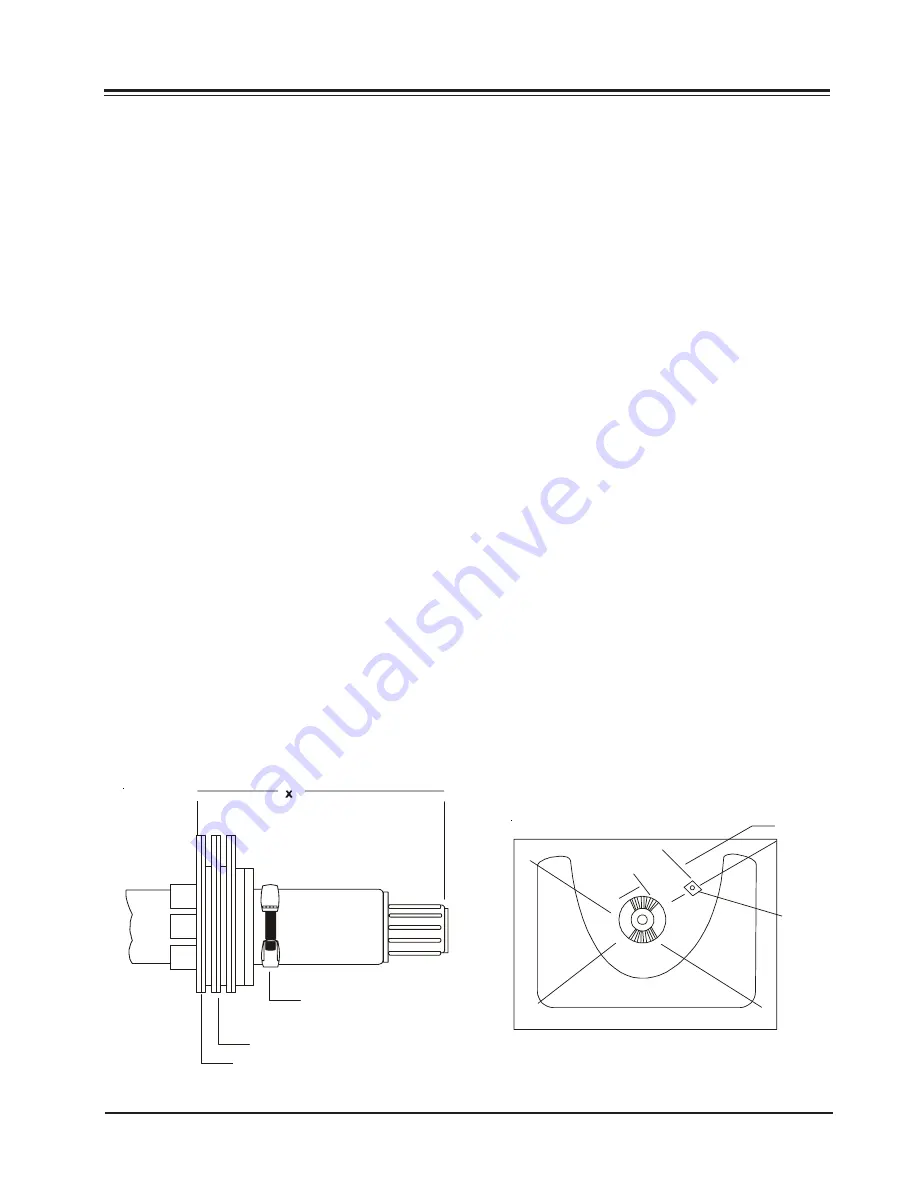
4 Pole Magnets

Clamp and Screw

6 Pole Magnets

2 Pole Magnets

2" To 3"

MAGNET

positions and secure each wedge with a

piece of tape, as described above.

IMPROVING CRT CORNER PURITY

CRTs that display corner purity prob-

lems even after following the service

procedures can be modified with a pic-

ture correction kit (P/N 949-00050).

The purity can be improved by placing a

picture-correction magnet (included in

the kit) on the CRT funnel. Refer to

the following modification steps and

illustration to place the magnet prop-

erly. Fully degauss the CRT before in-

stalling correction magnets.

MODIFICATION 1. Place the magnet on

the CRT funnel as shown in the figure

displayed below, in the quadrant ex-

hibiting impurity.

2. Rotate the magnet in place to the

position shown for best purity.

3. Place a piece of 1/2" by 2" long

Fiberglass tape over the magnet to hold

it in place.

4. Degauss the CRT once magnet is in

place to insure that the magnet is not

over the internal magnet shield.

Note: If the magnet is placed over the internal

magnet shield, any apparent purity
correction will disappear after degaussing.
Reposition the correction magnet off the

internal shield and degauss again.

Summary of Contents for H27G48S

Page 1: ...aller s Menu Servicing Trobleshooting Model Module Parts List Exploded Views Schematics Published by Technical Publications Zenith Electronics Corporation P O Box 240007 Huntsville Al 35824 Copyright May 2006 by Zenith Electronics Corporation Printed in U S A z e n i t h Presentation Series DIGITAL FCS 3828VD0171G H 2006 1 2 3 4 5 6 H27H49S H32H49S ...

Page 2: ...eled by 15 mfd 150V AC type capacitor between a known good earth ground water pipe conduit etc and the exposed me tallic parts one at a time Measure the AC voltage across the combination of 1500 ohm re sistor and 15mfd capacitor Reverse the AC plug by using a non polarized adaptor and repeat AC voltage measurements for each exposed metallic part Voltage measured must not exceed 0 75 volts RMS This...

Page 3: ...pping the Horizontal Drive Output H DRV pin 40 pulse train therefore shut ting down to Horizontal Output Fly Back trans former switching off the HV and horizontal de flection If the shutdown condition disappears the TV set can be turned on only if the AC is interrupted for about 20 Seconds and then the on off switch is activated CPT ANODE HIGH VOLTAGE MEASUREMENT PROCE DURE Each CPT screen size ha...

Page 4: ... TV is plugged into a cable box or a power outlet controlled by a wall switch Use ADJUST to select 0 or 1 where 0 is the default is OFF and 1 is ON NOTE When set to 1 ON the TV does not re spond to POWER On Off commands from either the remote or the TV front control panel and the SLEEP TIMER is also nonfunctional 3 I BAND AFC Band Automatic Frequency Control There are 8 possible settings for this ...

Page 5: ...MER When set to 1 the Sleep Timer feature is avail able to the user but no message is displayed prior to turn off When set to 0 the Sleep Timer is not functional 16 I EN TIMER Enable Timer Set to 1 On Off Timer functions are available to user Set to 0 to disable On Off Timer func tions Note Clock must be set in order to use Timers 17 I ALARM Gives you the option of making the alarm func tion avail...

Page 6: ... for M P I AUX source to be reported as a channel number instead of channel 0 Set to 0 to disable AUX identification change 48 I DIS SETUP M Disable Setup Menu Set to 1 to disable the Setup menu Setup menu will not appear Set to 0 to enable the Setup menu 49 I DIS AUDIO M Disable Audio Menu Set to 1 to disable the Audio menu Audio menu will not appear Set to 0 to enable the Audio menu 50 I DIS VID...

Page 7: ...ue 7 White 2 Green 5 Violet 68 I BCK SRC M Source Menu Background Color Set according to Color Chart 0 Black 3 Yellow 6 Cyan 1 Red 4 Blue 7 White 2 Green 5 Violet 69 I EN CH T COL Enable Channel Time Custom Color Set to 1 to enable custom color for the Channel Time display Set to 0 to disable custom color for the Channel Time display 70 I FOR CH T COL Channel Time Display Fore ground Color Set acc...

Page 8: ... NOT USED 98 I NOT USED 99 I NOT USED 100 I NOT USED 101 I NOT USED 102 I NOT USED 103 I NOT USED 104 I NOT USED 105 I NOT USED 106 I A RATIO LOCK Aspect Ratio Lock If set to 1 current picture aspect ratio is retained at power Off At power On previous aspect ratio will be used If set to 0 resets aspect ratio to default setting at TV turn On FACTORY MENU ACCESSING THE FACTORY S MENU Using the remot...

Page 9: ...settings have not been stored 003 F VERT POS Moves Captions and displays vertically on the screen Use the ADJUST keys 004 F HORZ POS Moves Captions and displays horizontally on the screen Use the ADJUST keys G2 ADJUSTMENT 005 F AIR AFT Enable Disable 1 0 This fea ture is for enable or disable the AFT execution in AIR Band 006 F G2 ADJUST Max value of 254d and default value of 127d It is required t...

Page 10: ...t setting for Aux video inputs Range 0 3 0 OFF 1 Low 2 Medium 3 High 037 F LTIMODE AUX Luminance transient im provement for aux video inputs Default value in 1 038 F SYSTEM AUX Signal frequency band switch ing select the band in accordance with the TV System Range 0 3 0 NORMAL 1 FF 2 HD 3 FIX HD setting which gives greater impor tance to frequency response than 2 039 F DCTRAN Y system DC transmiss...

Page 11: ...arity adjustment Range 0 15 Initial value 07 077 F V_S_CORRECTION Vertical S correction Range 0 15 Initial value 5 078 F UP_VLIN Vertical linearity control Range 0 15 Initial value 0 079 F LO_VLIN Vertical linearity control Range 0 15 Initial value 0 080 F H_SIZE Horizontal amplitude adjustment Range 0 63 Initial value 43 081 F H_POSITION Horizontal position adjust ment Range 0 63 Initial value 31...

Page 12: ...dow shift for fine error cal culation Default value in 0 no offset 115 F HUEM Tint control for NTSC signals 116 F AGCMDM AGC behavior can be chosen from four possible modes 117 F AGCADJ1M Automatic gain adjustment ADC1 118 F CLMPST1SM Measure pulse duration for ADC1 119 F CLMPHIGHM Vertical end of clamping pulse Default value is 255 Line 766 120 F CLMPLOWM Vertical start of clamping pulse Default ...

Page 13: ...fault value is 3 160 F HORWIDTHM_L Horizontal picture width Default value is 32 161 F VERWIDTHM_H Default value is 1 162 F VERWIDTHM_L Vertical picture width De fault value is 31 163 F PKCTIBPM AUX Band pass Peaking factor for CTI of Aux video inputs Default value is 3 164 F PKCTIHPM AUX High pass Peaking factor for CTI of Aux video inputs Default value is 2 165 F LTIM Luminance transient improvem...

Page 14: ...ity 0 positive 204 F HOUTPOL Horizontal output polarity 0 high active 205 F VOUTPOL Vertical output polarity 0 high active 206 F BLANPOL Blank polarity 0 high active 207 F VBLANDEL_95 Vertical delay in lines from in v sync Default value is 0 208 F BLANLEN_H Default value is 0 209 F BLANLEN_L Default value is 0 210 F VBLANDEL_40 Vertical length in lines from start of active blank signal Default val...

Page 15: ...MAX COLOR Max value of 63d and default value of 55d for 27 and 47d for 32 This value is used in one formula to limit the maximum color level 007 F RF SUB_TINT Max value of 15d and default value of 7d This value is used in one formula to center the tint level of RF input 008 F AUX SUB_TINT Max value of 15d and default value of 7d This value is used in one formula to center the tint level of composi...

Page 16: ...ex treme top edge Range 0 3 Initial value 0 042 F LO_UCP Horizontal pin adjustment for ex treme bottom edge Range 0 3 Initial value 0 043 F UP_UCG Horizontal pin gain adjustment for extreme top edge Range 0 3 Initial value 0 044 F LO_UCG Horizontal pin gain adjustment for extreme bottom edge Range 0 3 Initial value 0 045 F UC_POL Horizontal pin polarity setting for extreme top bottom edge Range 0 ...

Page 17: ...gnal De fault value is 3 076 F YFDEL Y delay adjustment Default value is 55d 077 F UVDEL UV delay adjustment Default value is 55d 078 F RGBSEL RGB input selection 0 Use RGB YUV input1 079 F USATADJ U saturation adjustment Default value is 40d 080 F VSATADJ V saturation adjustment Default value is 42d 081 F ADCSEL Select ADC for sync signal conver sion 0 Use ADC_G 082 F AABYP Bypass RGB YUV anti al...

Page 18: ...g for Component video input Range 0 3 0 OFF 1 Low 2 Medium default 3 High 109 F LTIMODE_YPRPB Luminance transient improve ment for component video input Default value in 1 110 F LTILEV_YC Luminance signal edge enhance ment setting for S Video inputs Range 0 3 0 OFF 1 Low 2 Medium default value 3 High 111 F LTIMODE_YC Luminance transient improve ment for S Video inputs Default value in 1 Y Pr Pb IC...

Page 19: ...5 VDC typical the control circuit enables regulator op eration Once the regulator output volt age is established the drive winding DX3601 starts to charge CX3605 via DX3601 The voltage on CX3605 thus re covers to the nominal drive voltage SWITCHED POWER SUPPLY START UP The voltage output of the rectifier BRX3400 V1 150VDC is supplied to the Main Switch Mode Regulator Power Supply SMPS The Main SMP...

Page 20: ... 40 high 60 low Current from H DRV is amplified by tran sistor Q3200 and Q3201 providing a low impedance to rapidly drive the gate of the drive transistor Q3203 This action results in an alternating cur rent flow in the primary of driver trans former TX3200 During Q3203 on time energy is stored in TX3200 and rapid turn off of QX3204 is initiated Dur ing Q3203 off time the energy previ ously stored...

Page 21: ...er the 4 pole control has been adjusted to superimpose the red and blue lines on top of one another Use the 6 pole static adjustment to place the converged red and blue lines over the green line Move the two tabs together around the neck of the CRT in a 30 arc from the top dead center position to move the lines vertically Adjusting the two tabs separately will move the converged beam to the left o...

Page 22: ...o clock position Follow through on the horizontal tilt adjustment by using the 2 and 10 o clock 4 Pole Magnets Clamp and Screw 6 Pole Magnets 2 Pole Magnets 2 To 3 MAGNET positions and secure each wedge with a piece of tape as described above IMPROVING CRT CORNER PURITY CRTs that display corner purity prob lems even after following the service procedures can be modified with a pic ture correction ...

Page 23: ...d IF 4 5MHz to the audio processor to be demodulated At the front jack pack one pair of audio jacks is used with both the Com puter and Aux Video inputs If both video inputs are in use the Aux Video is selected as default input The rear jack pack includes one set of audio jacks for the S Video another set of audio jacks for the Aux Video input and a third pair for the RGB Computer input The Audio ...

Page 24: ...al pro cessing It has sync signal automatic identification circuit with fixed mode Also receives the H V SYNC SCAN comes from SCAN CARD at pins 36 IN1_H L1 and 37 IN1_V L2 and the H V SYNC FRONT comes from front jack pack at pins 44 IN2_H L1 and 45 IN2_V L2 to be switched in itself The ICM2200 CXA2150Q I2C bus supported is a bi polar IC which integrates base band Y C signal processing RGB processi...

Page 25: ... scending input voltages The RGB output signals of this IC goes directly coupled to the input pins each power amplifier IC Pin 2 of IC5121 IC5141 and IC 5161 The core of the Red amplifier is IC5121 This IC is an operational amplifier configured as an inverting amplifier The inverting input is on pin 2 and the non inverting input is on pin 4 The Feedback resistor is R5125 The ampli fier has a gain ...

Page 26: ...r AL Radial 0CE475CK636 Capacitor AL Radial 0CE475DK618 Capacitor AL Radial 0CE476BK618 Capacitor AL Radial 0CE476DF618 Capacitor AL Radial 0CE476DH618 Capacitor AL Radial MODEL H27H49S PART NUMBER DESCRIPTION 0CE476DK618 Capacitor AL Radial 0CE476DR618 Capacitor AL Radial 0CE476EU61A Capacitor AL Radial 0CE476SF6DC Capacitor AL Chip 0CE476VF6DC Capacitor AL Chip 0CE477BH618 Capacitor AL Radial 0C...

Page 27: ...bon Film 0RD0152H609 Resistor Carbon Film 0RD0331F609 Resistor Carbon Film 0RD0392H609 Resistor Carbon Film MODEL H27H49S PART NUMBER DESCRIPTION 0RD0472F609 Resistor Carbon Film 0RD0752F609 Resistor Carbon Film 0RD1000F609 Resistor Carbon Film 0RD1001F609 Resistor Carbon Film 0RD1001H609 Resistor Carbon Film 0RD1002F609 Resistor Carbon Film 0RD1003F609 Resistor Carbon Film 0RD1003H609 Resistor Ca...

Page 28: ...sembly 180 A01A Resistor Wire Wound 180 C02M Resistor Carbon Composition 181 007C Capacitor Film DIP 181 007H Capacitor Film DIP 181 009D Capacitor Film DIP MODEL H27H49S PART NUMBER DESCRIPTION 181 009V Capacito Drawing 181 010E Capacitor Film DIP 181 010G Capacitor Film DIP 181 010H Capacitor Film DIP 181 013U Capacitor Film DIP 181 014N Capacitor Film DIP 181 014Y Capacitor Film DIP 181 015D Ca...

Page 29: ... 0CE106VF6DC Capacitor AL Chip MODEL H32H49S PART NUMBER DESCRIPTION 0CE107DF618 Capacitor AL Radial 0CE107DH618 Capacitor AL Radial 0CE107DJ618 Capacitor AL Radial 0CE107DK618 Capacitor AL Radial 0CE107SF6DC Capacitor AL Chip 0CE108BJ618 Capacitor AL Radial 0CE108DD618 Capacitor AL Radial 0CE108DF618 Capacitor AL Radial 0CE108DH618 Capacitor AL Radial 0CE108DH630 Capacitor AL Radial 0CE108DJ618 C...

Page 30: ... Sound Audio Processor MODEL H32H49S PART NUMBER DESCRIPTION 0IMCRMN029B IC Unclassified 0IMCRMZ001A IC DC DC Converter 0IMCRSG010A IC Transceiver 0IMCRSG011A IC Voltage Regulator 0IMCRSJ001B IC LDO Voltage Regulator 0IMCRSO007A IC Micro Controller 0IMCRSO008A IC Graphic Controller 0IMMRHY060B IC DDR SDRAM 0IPH488700A IC Pre Amplifier 0IPH612000B IC Video Amplifier 0IPMGSK019A IC PWM Controller 0I...

Page 31: ...09 Resistor Metal Oxide Film 0RS0121K607 Resistor Metal Oxide Film 0RS0151K607 Resistor Metal Oxide Film 0RS0221H609 Resistor Metal Oxide Film 0RS0221K607 Resistor Metal Oxide Film 0RS0391K607 Resistor Metal Oxide Film 0RS0472H609 Resistor Metal Oxide Film 0RS1000H609 Resistor Metal Oxide Film MODEL H32H49S PART NUMBER DESCRIPTION 0RS1001H609 Resistor Metal Oxide Film 0RS1003K607 Resistor Metal Ox...

Page 32: ...70VMCA12P Transformer Switching 6170VMCA582 Transformer Switching 6174V 6012N Transformer BT 6200C000026 Filter Saw 6200C000027 Filter Ceramic 6200C000028 Filter Unclassified 6201V00002A Filter Assembly 6204B62705A Oscillator Crystal 6210TCE001A Filter Bead 6210VH0001A Filter Ferrite Core 6212AA2984B Crystal 6212AA2988A Resonator Crystal 6212AB3004D Resonator Ceramic 6212BA3010A Resonator Ceramic ...

Page 33: ......

Page 34: ......

Page 35: ......

Page 36: ...S AS S E M BLY K E Y BO AR D 3141V S NC 61H 4 W IND O W 3790V 00705A 5 C P T AS S E M BLY C R T 6335V 29025J 6 BAC K C O V E R AS S E M BLY 3809V 00B05F 7 C HAS S IS AS S E M BLY M AIN S M P S 3141V F N003A 8 R E M O T E C O NT R O LLE R 6710V 00121A PRG POWER VCR CABLE SURF FLASHBK MUTE TV AUX CHANNEL CHANNEL VOLUME 3 2 1 4 5 6 7 8 9 0 ENTER MENU A B C C C R C E ORD ND EWI R P U E S A T R IME LAY...

Page 37: ...MBLY 3809V00343E 7 CHASSIS ASSEMBLY MAIN SMPS 3141VFN003C 8 REMOTE CONTROLLER 6710V00121A H32G48S Exploded View 5 2 3828VD0171E FCS 48 SERIES SHEET 2 1 2 3 4 5 6 7 8 9 10 MBR3447C 6710V00121A 124 00233 04 PRG POWER VCR CABLE SURF FLASHBK MUTE TV AUX CHANNEL CHANNEL VOLUME 3 2 1 4 5 6 7 8 9 0 ENTER MENU A B CC C R C E ORD ND E I R W P U E S A T R IME AY L P FW FD TOP S TV C V R OU C S R E QUIT VOLU...

Page 38: ...ED VIDEO IN BLUE VIDEO IN GREEN VIDEO IN H SYNC V SYNC R OSD G OSD B OSD FB OSD SCL 2 2 1 MPI DIN3 MPI DOUT4 SPI DOUT5 SPI DIN6 SPI CLK7 8 9 IR DATA OUT H SYNC SCAN B FRONT G FRONT R FRONT HORZ FRONT VERT FRONT G SCAN B SCAN R SCAN CN3C9 CN6F2 IC800 IC1400 CN1B2 CN1A2 CN1C2 CN2B1 LARGE SIGNAL SMALL SIGNAL CN8B4 CN2F6 CN1 GND2 CN6K2 CN5K2A CN6P2A 27V MODEL SW100 CN2C1 CN2C9 CN4C9 CN2D1 CN1D2 QX3205...

Page 39: ...V RM2923 PROV C2925 50V 1µ F R2924 5 6K R2926 47 CM2927 50V PROV CM2928 50V PROV 2 1 4 5 3 DL2400 1 HCF0361 VID IN C OUT GND VCC Y OUT 6200C000032 CM2402 50V 100pF CM2403 50V PROV Q2903 E B C KSC945C Y 0TR945009AA C2411 16V 47µ F Q2904 E B C KSC945C Y 0TR945009AA CM2935 50V PROV Q2905 E B C KSC945C Y 0TR945009AA L2905 15µ H CM2945 50V PROV CM2936 50V PROV C2937 16V 220µ F L2900 47µ H CM2401 50V 33...

Page 40: ... 2 7 10 0 CM2252 50V 2200pF RM2242 2K C2209 16V 220µ F D2200 1N4148 0DD414809ED D2201 1N4148 0DD414809ED Q2205 E B C BF959 0TR959009AA H FB P CLAMP AB L 1 2 3 4 CN4C9 1 366 921C CM2253 100pF 50V RM2239 1 8K RM2273 100K RM2274 100K HORZ SW RM2275 1K C2241 50V 10µ F C2242 50V 10µ F CM2243 50V 33PF CM2244 50V 33PF VM C ORR 2 14 13 1 12 11 10 9 8 7 6 5 4 3 Q1 R1 D1 CP1 S1 Q1 VCC GND Q2 Q2 S2 CP2 D2 R2...

Page 41: ...3 100 RM2754 100 RM2755 100 RM2756 100 ADDRESS IN1_ V L2 SDA SC L NC Vcc2 SELYOUT SELC B OUT SELC ROUT GND2 SELVOUT SELHOUT NC IREF NC EXTCLK XTAL NC YGIN YGOUT V_ PH H_ PH 24 13 14 23 22 12 11 10 9 8 7 21 20 19 6 5 18 17 16 15 36 35 4 1 34 3 33 2 Vcc3 IN4_ V IN4_ H IN4_ 3 IN4_ 2 IN4_ 1 GND3 IN3_ V IN3_ 3 IN3_ H IN3_ 2 IN3_ 1 32 31 30 29 28 27 26 25 37 38 47 46 IN1_ H L1 IN1_ L3 IN1_ SW Vcc1 IN2_ ...

Page 42: ... IN ICM2701 BA7657F NEW 1 2 3 4 5 6 7 8 9 10 11 12 24 23 22 21 20 19 18 17 16 15 13 14 GND B OUT HD OUT B2 IN GND VD2 IN CTL VCC HD2 IN GND VD1 IN GND VD OUT CV IN G2 IN G OUT R OUT R2 IN B1 IN HD1 IN COMP SYNC OUT G1 IN SYNC DET R1 IN ICM2702 BA7657F NEW CM2704 25V 0 01 CM2706 25V 0 01 CM2702 25V 0 01 CM2724 25V 0 01 RM2737 PROV R G B SVM OUT 1 2 3 4 5 8 7 6 CN2C9 1 366 921G RM2702 1K RM2701 1K R...

Page 43: ...2002 10µ H CRY2001 HCU 00139 20 25MHz 6212AA2988A Q2004 2N7000 G D S 0TFON80002A Q2005 2N7000 G D S 0TFON80002A CM2013 50V PROV CM2018 16V 0 1 CM2019 16V 0 1 CM2020 16V 0 1 CM2026 16V 0 1 CM2027 16V 0 1 RM2018 0 1 CM2001 16V 0 1 CM2002 16V 0 1 C2014 16V 22µ F CM2005 50V 27pF CM2006 16V 0 1 CM2009 16V 0 1 CM2010 16V 0 1 CM2011 16V 0 1 CM2012 16V 0 1 CM2017 3 0 1 RM2007 100 RM2013 4 7K RM2008 75 RM2...

Page 44: ...T T1 1 12 TLT 12 TLT 5V TNR 5V TNR 5V TNR PROTEC TION NC SW1 SW2 Vc c 1 Vc c 2 OUT2 OUT1 PROTEC TION GND 7 8 6 5 3 4 2 1 9 10 IC4500 LB1645N 1 0ISA164500B C4502 50V 47µ F Q4500 KTC3198 E B C 0TR319809AA C4503 50V 4 7µ F D4500 1SS133 0DS113379BA Q4501 KTC3198 E B C 0TR319809AA R4501 1K R4505 100 1 2 3 CNTILT 1 366 921B C4500 50V 0 1 C4501 16V 0 01 R4507 12K R4506 10K R4504 10K R4502 100 Q4502 KTC31...

Page 45: ...6 RM1232 100K RM1233 100K RM1200 100K CM1206 50V 1000pF C1228 50V 0 22 CM1227 50V 0 01 1 2 3 4 5 6 7 8 9 15 2 0 19 13 14 10 11 16 12 17 IF AGC 1 EQ AMP VIF IN1 18 LEVEL REF SIGNAL RF AGC AUDIO AFT IF AGC 2 VIF IN2 GND F B SIF OUT SIF IN OUT VC O F B APC VIDEO DET LOGIC VC C AUDIO VIDEO OUT VIDEO IN VC C IC M12 0 0 M6 1113 FP NEW RM1231 PROV L1209 10µ H Q1203 BF959 E B C 0TR959009AA CM1232 50V PROV...

Page 46: ...C1401 KA7533ZTA GND VCC OUT 0IFA753307A 1 2 3 CN9L4 1 366 921B R1402 100 Q1400 E B C KSA733C Y 0TR733009AA Q1401 E B C KSA733C Y 0TR733009AA Q1404 E B C KSA733C Y 0TR733009AA Q1403 E B C KSA733C Y 0TR733009AA Q1402 E B C KSC945C Y 0TR945009AA 1 2 3 4 CN9R4 366 921C 1 C801 50V 0 1 C813 50V 0 1 C823 0 1 50V R1401 100 RM1417 PROV R1418 1 5K R1414 1 5K RM1413 PROV R813 3 3 R823 3 3 C1400 50V 3 3µ F C1...

Page 47: ...cc RVCO 51 DEG CTL 50 49 48 47 6 5 4 3 2 1 G R B FB HLF VSS XOUT XIN CAMPORT SENSE RESET SDA2 COMPUTER SENSE TILT2 TILT1 N C N C MUTE A D_ KEY2 AVcc SDA1 SCL1 CNVSS CONTROL1 SPI DIN A D_ KEY1 IR DET SCL2 HSYNC SIGN MTR H DET SP1 CLK N C CONTROL2 V DET SCAN RESET FS VSYNC AFT N C SIGNAL DETECT N C SP1 DOUT IC6000 1 M37278 NEW IC6002 KIA7042P AT 1 VCC OUT 0IKE704200B L6000 1µ H L6001 1µ H R6066 470 ...

Page 48: ...V 2200µ F IC X3821 KIA78R05PI IN OUT GND 5V 0IKE7805001 IC X3822 IC X3822 IC X3823 4920V00022 CTL ICX3823 4921 NEW RX3826 2W 3 3 RX3834 4 7K CX3831 16V 47µ F CX3837 16V 470µ F IC X3821 KIA78R05PI IN OUT GND 5V 0IKE7805001 IC X3822 ICX3822 IC X3823 4920V00022 CTL IC X3823 4921 NEW CX3832 16V 47µ F RX3835 680 ICX3821 KIA78R05PI IN OUT GND 5V 0IKE7805001 ICX3822 ICX3822 ICX3823 4920V00022 CTL ICX3823...

Page 49: ... 01 1 2 CX3229 2KV 2200pF CX4806 1600V 8200pF C3219 1000V 560pF 1 2 3 Q3203 IRFS630B G D S 0TF630000CB 1 2 R3244 2W 470 1 2 R3230 1 2W 1K 1 2 R3242 1 2W 1K 1 2 R4803 10K 1 2 R4805 220 1 2 R4809 10K 1 2 R4814 1 2W 15K 1 2 R4816 1 2W 510 1 2 RX3234 P L 1 2W 1 2 RX2101 2W 1 1 2 RX2108 1W 2 7 1 2 RX2109 1W 2 7 1 2 RX2110 1 2W 680 1 2 RX2111 1 2W 680 1 2 RX3233 2W P L 1 2 RX3235 2W 0 47 1 2 RX3236 1 2W...

Page 50: ...1 2 RX3411 1 2W 470K CX3417 4KV 2200pF CX3416 KV 2200pF RX3400 1 2W 8 2M LX3400 LFZ35V04 6140VB0012B 18m H CX3406 250V 220µ F CX3407 1000V 470pF 1 2 RX3900 2 2K 1 2 3 QX3900 E B C KTC3228 0 0TR322809AA 1 2 DX3900 GUF10J 0DRGF00104A 1 2 3 4 KX3900 12V DG12D1 O M 141 018E 1 2 DX3870 0DRGF00104A GUF10J 1 2 3 4 KX3870 12V DG12D1 O M 141 018E 1 2 3 QX3870 E B C KTC3228 0 0TR322809AA 1 2 RX3870 2 2K 1 2...

Page 51: ...13 14 15 16 17 18 18 15 13 11 10 9 7 5 6 4 2 1 TX3670 1 EER4954S NEW 1 2 RX3856 1 2W 5 6 1 2 CX3858 50V 0 47 1 2 CX3860 50V 220µ F 1 2 3 4 5 5 4 3 1 2 ICX3670 OCP FB STR F6658B GND 0ISK665813A VIN 408 003C D S 4921V00188L 1 2 3 ICX3851 KIA7808API IN OUT GND 8V 150m A 0IKE780800J 1 2 CX3857 50V 0 47 1 2 CX3853 25V 470µ F 1 2 FX3663 Type MS3 125V 3A SLOW BLOW MFD BY BELL FUSE 0FS3001A282 1 2 RX3854 ...

Page 52: ...00 LTV817M VB 1 0ILI817000G 1 2 3 4 5 6 7 8 5 6 7 8 4 3 2 1 N C SOURC E START UP OLP D FB VC C OC P D GND ICX3612 01 STR A6151 4 0IPMGSK019A 1 2 RX3602 33K 1 2 ZDX3602 MTZJ5 6B 1 2W 5 6V PROV 1 2 CX3602 50V 4 7µ F 1 2 CX3603 50V 220pF 1 2 CX3604 50V 470pF 1 2 3 R C A ICX3701 KA431LZ 0ICTMFA001A 1 2 RX3703 0 1 1 4W 3 57K 1 2 RX3702 33K 1 2 RX3700 1 2W 680 1 2 S F LX3610 150 C02F 82µ H 1 2 CX3702 50...

Page 53: ... 1 2 3 4 5 6 7 8 9 10 11 MPI_ DATA_ IN MPI_ DATA_ OUT CLONESENSE PTY SELECT 11 10 9 8 7 6 5 4 3 2 1 CON11E1 6630VL02811 1 1 2 3 4 5 6 6 1 5 2 3 4 MPI 6612VEH001A 1 1 2 3 Q4903 E B C 0TR733009AA KSA733C Y 1 2 3 Q4904 E B C 0TR945009AA KSC945C Y 1 2 3 Q4905 E B C 0TR945009AA KSC945C Y 1 2 3 Q4906 E B C 0TR945009AA KSC945C Y 1 2 R4985 470 1 2 R4983 1M 1 2 R4984 1K 1 2 R4986 22K 1 2 R4987 3 3K 1 2 R49...

Page 54: ...EIR COMPONENTS DESIGNATORS REPLACE ONLY WITH PART NUMBERS SPECIFIED ALL COMPONENTS WITH M IN THE DESIGNATOR ARE A SURFACE MOUNTED COMPONENT 3828VD0171E FCS 48 SERIES SHEET 17 11 10 9 8 7 6 5 4 3 2 1 CN3 6630VL02711 11 10 9 8 7 6 5 4 3 2 1 CN2 6630VL02711 16 17 8 6 3 2 5 4 10 7 12 1 15 11 14 13 9 J1 1 6630GL00515 SHT 6 19 ...

Page 55: ...12 CN9C3 366 921L 1 2 3 4 H FB P VDO CLAMP AB L 1 2 3 4 CN9C4 1 366 921C D5104 PROV 1 2 3 4 5 6 7 8 9 10 11 12 24 23 22 21 20 19 18 17 16 15 13 14 SCL GND VP1 VoG LIM CL1 VP2 FB RB VinR VP VinG GND VinB HFB SDA VoB FB RG FB RR VoR B OSD G OSD R OSD FBL VP3 IC5101 TDA4886 NEW 1 2 L5102 10µ H 1 2 R5136 10K R5131 100 R513 100 1 2 R5137 12K 1 2 R5138 150 1 2 R5139 10K 1 2 R5140 270K 1 2 R5141 270K R51...

Page 56: ...7 6 5 4 3 2 1 CN1E11 6630VL02711 12LSP PS GND MPI DIN MPI DOUT SPI DATA OUT SPI DATA IN SPI CLOCK DATA GND 5VUP IR DATA OUT 1 2 3 4 5 8 7 6 9 10 CN1VGA10 366 922J SPARE AUDIO GND RED VIDEO IN RIGHT AUDIO IN LEFT AUDIO IN GREEN VIDEO IN BLUE VIDEO IN H SYNC V SYNC 11 10 9 8 7 6 5 4 3 2 1 CN2E6 6630VL02711 SPARE AUDIO GND RED VIDEO IN RIGHT AUDIO IN LEFT AUDIO IN GREEN VIDEO IN BLUE VIDEO IN H SYNC ...

Page 57: ...1 2 E5121 6918VAX002E 350V 1 2 E5122 PROV 350V 1 2 E5141 6918VAX002E 350V 1 2 E5161 6918VAX002E 350V 1 2 3 4 5 6 7 8 9 10 11 12 13 14 15 OUT OUTO NC 2 0 0 V NC GND IK 12 V IIN VB RC VIN RC 9 8 7 6 5 4 3 2 1 10 11 12 13 IC5121 TDA6120Q 4921V00181V 1 1 2 3 4 5 6 7 8 9 10 11 12 13 14 15 OUT OUTO NC 2 0 0 V NC GND IK 12 V IIN VB RC VIN RC 9 8 7 6 5 4 3 2 1 10 11 12 13 IC5141 TDA6120Q 4921V00181V 1 14 ...

Page 58: ...T IN 1 2 3 4 5 8 7 6 CN8B4 366 921G 1 2 3 4 5 6 7 7 6 4 3 2 1 AUDIO LEFT IN VIDEO IN AUDIO RIGHT IN 5 JP1 1 PJ 6054 NEW Front Jack Circuit 1 2 3 4 5 6 7 8 9 10 G D C B E F A 6 21 CRITICAL SAFETY COMPONENTS ARE IDENTIFIED BY THE LETTER X IN THEIR COMPONENTS DESIGNATORS REPLACE ONLY WITH PART NUMBERS SPECIFIED ALL COMPONENTS WITH M IN THE DESIGNATOR ARE A SURFACE MOUNTED COMPONENT 3828VD0171E FCS 48...

Page 59: ...RE A SURFACE MOUNTED COMPONENT 3828VD0171E FCS 48 SERIES SHEET 22 5V SB 5V SB 5V SB 5V SB 5V SB 1 2 3 4 5 CN2K5 387 A05B 1 2 3 4 5 CN6K2 387 A05E R5 10K R6 10K R7 1K R8 1K R9 1K R10 1K R11 1K R12 1K R13 1K R14 1K R15 1K R16 1K 1 SW2 140 315A 1 2 SW3 140 315A 1 2 SW4 140 315A SW5 140 315A SW6 140 315A SW7 140 315A UP VOLUME CHANNEL UP VOLUME TO MAIN PCB MENU CLOSED CAPTION DOWN TO IR LED POWER PCB ...

Page 60: ... C2 35V 4 7µ F 1 2 C200 35V 4 7µ F 1 2 3 4 5 1 2 3 4 5 CN5K2 1 366 921D 1 2 3 4 5 1 2 3 4 5 CN5K2A 1 366 921D 1 2 3 1 2 3 CN6P2 387 P L 1 1 2 3 1 2 3 CN6P2A 387 P L 1 1 2 3 IR1 GND GND VCC OUT 6726VV0006J 1 2 3 IR100 GND GND VCC OUT 6726VV0006J 1 2 LED1 162 002B 1 2 LED100 162 002B 1 2 R1 750 1 2 R2 100 1 2 R3 330 1 2 R4 10K 1 2 R100 750 1 2 R200 100 1 2 R300 330 1 2 R400 10K 1 2 3 4 5 6 7 8 SW1 1...

Page 61: ...RM6 0 0 9 RM6 0 5 9 RM6 0 6 0 RM6 0 5 7 RM6 0 5 8 RM6 0 5 5 RM6 0 5 6 C M6 0 2 9 C M6 0 3 5 C M6 0 14 C M6 0 15 C M6 0 17 C M6 0 18 C M6 0 2 0 C M6 0 2 1 RM6 0 2 9 C M6 0 2 3 C M6 0 4 0 C M6 0 4 2 C M6 0 4 1 C M6 0 4 3 C M6 0 4 4 C M6 0 5 1 C M6 0 5 2 C M6 0 5 3 C M6 0 5 0 C M6 0 4 8 C M6 0 0 4 C M6 0 0 5 C M6 0 0 6 C M6 0 10 C M6 0 4 7 C M6 0 11 C M6 0 12 C M6 0 13 C M6 0 4 5 C M6 0 4 6 C M6 0 2 ...

Page 62: ...L1204 L1203 Q1200 E B C C 2 0 2 2 53 C2750 C 2 7 15 C812 C822 GNDA1 GNDC1 GND1B D2202 FID12 FID13 FID14 FID15 FID16 FID17 FID18 FID24 FID25 FID26 FID27 FID28 D2 0 0 0 1 C2762 C2014 C2761 AGC CHECK PROCESS DIRECTION PROCESS DIRECTION MAY 11 2004 CN2B1 CN2C1 1 C X3 8 3 2 RX3836 RX3 8 2 7 RX3920 RX3 8 2 2 IC800 1 11 CN9L4 1 C 824 C823 R8 2 3 C X3 8 3 3 C X3 8 7 1 1 C 2 2 3 4 C2211 C 2 2 10 C2246 C220...

Page 63: ...3 8 5 0 W26 G6 8 W43 GNDB1 RX3411 DX3 6 5 3 CX3414 B RX3410 GN GND6A GND7 A DX3655 GND8A GND9A G72 RX3656 G7 4 G7 5 G76 C X3 9 0 0 G28 G29 HOT C OLD COLD C OLD HOT COLD C OLD C OLD HOT HOT HOT HOT HOT C OLD COLD HOT COLD HOT COLD HOT DIRECTION PROCESS C X4 8 0 7 C X3 2 0 4 A QX3204 E B C DX3202 R3245 CX3205 C X3 2 0 3 C X3 2 0 4 W6 25 R3 2 0 5 R3 2 12 226 C 3 2 0 1 FB 3 2 0 3 Q3 2 0 3 G D S C3220 ...

Page 64: ... M5 112 C M5 113 CM5115 C M5 116 C M5 117 CM5121 C M5 12 3 C M5 12 4 C M5 12 5 C M5 14 7 CM5130 CM5131 CM5132 CM5133 C M5 14 1 C M5 14 3 C M5 14 4 C M5 14 5 C M5 16 7 C M5 16 1 C M5 16 3 C M5 16 4 C M5 16 5 RM5 15 7 RM5 12 2 RM5 12 4 RM5 14 2 RM5 14 4 RM5 15 5 RM5 15 8 RM5 16 2 RM5 10 7 RM5 15 6 RM5117 RM5118 RM5 12 3 RM5119 RM5130 RM5 14 3 RM5163 RM5 16 4 RM5103 RM5113 G GND B OSD FB OSD GND R GN...

Page 65: ...5134 C5135 C5136 C 5 14 6 C 5 16 6 L5 10 4 CN3C1 C N9 C 2 C N9 C 3 C N9 C 4 1 C RT1 C R T 2 D5 10 1 D5102 D5103 D5104 D5 12 2 D5 14 2 DAG1 DAG2 E5121 E5 12 2 E5 14 1 E5161 L5 10 3 IC 5101 IC5121 1 IC5141 1 IC5161 1 L5 10 1 L5 10 2 R4 9 8 6 L5105 R5120 L5121 L5 14 1 L5 16 1 Q5 10 1 E B C Q5102 E B C R5 10 1 R5106 R5108 R5109 R5 110 R5 111 R5 12 5 R5 12 6 R5127 R5128 R5 13 1 R5 13 3 R5135 R5136 R513...

Page 66: ...z e n i t h ...

Reviews: