10
Fox (LP3500)
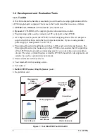
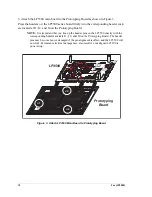
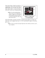
3. Attach the LP3500 main board to the Prototyping Board as shown in Figure 3.
Press the headers on the LP3500 series board firmly into the corresponding header sock-
ets located at J1, J2, and J4 on the Prototyping Board.
NOTE:
It is important that you line up the header pins on the LP3500 exactly with the
corresponding
header sockets
J1, J2, and J4
on the Prototyping Board. The header
pins may become bent or damaged if the pin alignment is offset, and the LP3500 will
not work. Permanent electrical damage may also result if a misaligned LP3500 is
powered up.
Figure 3. Attach LP3500 Main Board to Prototyping Board
GND RxE TxE
GND RxC TxC GND RxB
TxB GND + 485 GND +K OUT9 OUT8 OUT7 OUT6 OUT5 OUT4 OUT3 OUT2 OUT1 OUT0
GND
VIN GND
VBAT EXT
GND PWM2 PWM1 PWM0
GND AIN7
AIN6 AIN5
AIN4 AIN3
AIN2 AIN1
AIN0 GND
IN15
IN
14
IN
13
IN
12
IN
11
IN1
0
IN09
I
N08
G
ND
IN
07
IN
06
IN
05
IN0
4
IN0
3
IN0
2
IN01
I
N00
G
ND
J2
J21
J22
J23
J11
J12
J1
J13
J41
J42
J4
J43
J44
GN
D
VIN
LP3500
Prototyping
Board
S1
S2
S3
S4
RN1
DS
4 D
S3
D
S2
D
S1
D1
PW
R
J5
R1
VIN
GN
D
VIN
GND
VIN
GND
VIN
GN
D
GND
VIN
J3
3 V VBAT
J2
J4
J1
JP1
JP2
JP3
JP4
JP5 JP6
JP8
JP11 JP7
JP1
0
JP9
JP1
2
RP1
D3
RP2
D6
D12
D10
RP4
RP3
D16
D14
Q3
Q4
D23
D24
Q7
D27
Q9
RP10
D29
Q11
D31
Q15
RP12
RP11
Q21
Q19
Q18
PROGRAM
PORT
TP2
/RESET
RESET
S2
R14
C14
R15
C9
R5
R8
C27
R19
R21
R27
R24
C34
R28
C38
R35
C25
C31
C18
C28
C30
RP9
RP8
R59
C49
R52
R53
C63
R46
U2
815
07
IN
R10
R11
R12
R2
R3
R4
+K
GND
VCC
U6
U7
C42
C41
D9
C7
C5
C1
C4
C69
C68
C23
C17
Summary of Contents for Fox LP3500
Page 1: ...Fox LP3500 C Programmable Single Board Computer User s Manual 019 0111 041029 E ...
Page 6: ...Fox LP3500 ...
Page 14: ...8 Fox LP3500 ...
Page 22: ...16 Fox LP3500 ...
Page 86: ...80 Fox LP3500 ...
Page 120: ...114 Fox LP3500 ...
Page 130: ...124 Fox LP3500 ...
Page 134: ...128 Fox LP3500 ...
Page 138: ...132 Fox LP3500 ...
Page 142: ...136 Fox LP3500 ...
Page 144: ......


