background image

10GBASE-KR Ethernet TRD

8

UG1058 (v2017.1) April 19, 2017

www.xilinx.com

Chapter 1:

Introduction

• Ethernet Controller application GUI/Driver:

°

Provides a graphical user interface running on the control computer to pass user 

inputs to the 10GBASE-KR TRD and to display status through the KCU1250 board 

USB-to-UART port.

• Eye scan system:

°

AXI DRP bridge:
- Custom logic that allows access to DRP registers of the transceiver through any 

AXI master such as the MicroBlaze processor subsystem.

°

AXI block RAM controller:
- An AXI slave IP core that allows access to local block RAM by AXI master devices 

such as the MicroBlaze processor subsystem and the JTAG to AXI Master IP core.

- The block RAM stores the data read from the DRP port of the transceiver.

°

JTAG to AXI Master:
- An AXI Master IP core that can generate AXI transactions and drive AXI signals 

internal to FPGA in the system.

- Communicates with the AXI block RAM controller via the AXI Interconnect.
- Allows the Vivado® tools logic analyzer Tcl console running on the control 

computer to interact with FPGA through the USB-to-JTAG port on the KCU1250 

board.

°

MicroBlaze processor subsystem:
- An AXI Master that communicates with the AXI DRP bridge and AXI block RAM 

controller via the AXI Interconnect.

- Drivers running on the MicroBlaze processor subsystem implement an algorithm 

to measure a statistical eye (bit error ratio (BER) versus time and voltage offset). 

Data sampling points are available to read via the DRP port of the transceiver. 

Point-by-point measured data is stored in a block RAM to be burst read by the 

control computer via the JTAG to AXI Master.

°

AXI Interconnect:
- Allows multiple AXI masters (MicroBlaze processor subsystem and JTAG to AXI 

Master) to communicate with multiple AXI slaves (AXI DRP Bridge and AXI block 

RAM controller).

Send Feedback

Summary of Contents for KCU1250 10GBASE-KR

Page 1: ...KCU1250 10GBASE KR Ethernet TRD User Guide KUCon TRD05 Vivado Design Suite UG1058 v2017 1 April 19 2017...

Page 2: ...2015 4 with version 2016 1 11 23 2015 2015 4 Replaced all references to Vivado Design Suite version 2015 3 with version 2015 4 10 02 2015 2015 3 Replaced all references to Vivado Design Suite version...

Page 3: ...am the Clocks Sources 22 Program the FPGA 23 Configure VIO 25 Running the Design 31 Forward Error Correction 38 Dynamic Reconfiguration Ports 42 Chapter 4 Implementing and Simulating the Design Implem...

Page 4: ...4 UG1058 v2017 1 April 19 2017 www xilinx com Appendix D Additional Resources and Legal Notices Xilinx Resources 89 Solution Centers 89 References 89 Training Resources 91 Please Read Important Legal...

Page 5: ...to set up operate test and modify the design 10GBASE KR TRD Overview The 10GBASE KR TRD Figure 1 1 targets the Kintex UltraScale XCKU040 2FFVA1156C FPGA running on the KCU1250 characterization board...

Page 6: ...Generator and Monitor block and reports Ethernet performance It passes this information to the Ethernet Controller application GUI running on the control computer via the USB to UART port on the KCU1...

Page 7: ...n the user interface running at 156 25 MHz Is monitored through an AXI4 Lite interface Traffic Generator and Monitor Generates Ethernet traffic Monitors bandwidth utilization on the transmit and recei...

Page 8: ...XI transactions and drive AXI signals internal to FPGA in the system Communicates with the AXI block RAM controller via the AXI Interconnect Allows the Vivado tools logic analyzer Tcl console running...

Page 9: ...se these numbers as a rough estimate of resource utilization These numbers might vary based on the version of the 10GBASE KR TRD and the tools used to regenerate the design Table 1 1 10GBASE KR TRD Re...

Page 10: ...d A plug to micro B plug Power Supply 100 VAC 240 VAC input 12 VDC 5 0A output Backplane Z Pack TINMAN Customer System kit from Tyco Electronics Ref 3 Two Samtec Bulls Eye cables from Avnet Ref 4 Four...

Page 11: ...ivado Design Suite User Guide Release Notes Installation and Licensing UG973 Ref 8 Note Snapshots of the Vivado integrated design environment IDE in this document are from an older version of Vivado t...

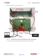
Page 12: ...SW1 to the OFF position SW1 in Figure 2 1 2 Connect the KCU1250 board to the control computer and power supply as shown in Figure 2 1 TIP Figure 2 1 shows only the top edge of the KCU1250 board 3 Powe...

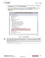
Page 13: ...ndard COM Port and then click Properties TIP Make note of the COM port numbers assigned by the control computer OS in your setup to Silicon Labs CP210x USB to UART Bridge Standard COM Port and Silicon...

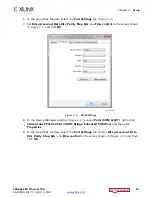
Page 14: ...in Figure 2 3 and click OK 8 In the Device Manager window Figure 2 2 expand Ports COM LPT right click Silicon Labs CP210x USB to UART Bridge Enhanced COM Port and then click Properties 9 In the prope...

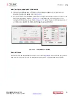
Page 15: ...erm connection and serial port settings as shown in Figure 2 4 These settings must match the control computer COM port settings shown in Figure 2 3 Select the serial COM port associated with Silicon L...

Page 16: ...rd software GUI Figure 2 5 2 Right click either the EthernetController 32 installer for a 32 bit operating system or EthernetController 64 installer for a 64 bit operating system and select Run as adm...

Page 17: ...2 6 click I Agree to continue installation 5 Browse to the location where the Ethernet Controller application will be installed and click Install Figure 2 7 X Ref Target Figure 2 6 Figure 2 6 License...

Page 18: ...ion after design bring up open the Control Panel In the Control Panel click All Control Panel Items Programs and Features and uninstall program Xilinx Ethernet Controller Powered by Xilinx Ready to Br...

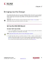
Page 19: ...before performing the bring up procedures described in this chapter Set Up the KCU1250 Board Connect Bulls Eye Cables 1 Connect the SAMTEC Bulls Eye cables to J41 GTH Transceiver Quad_226 and J42 GTH...

Page 20: ...out pins of Oscillator Si570 on the Superclock module 5 Connect the power supply to the KCU1250 board 6 Connect one end of the Micro USB cable to USB UART port J1 and the other to the Control PC 7 Con...

Page 21: ...e Backplane Power Supply 100VAC 240VAC Input 12 VDC 5 0A Output Board Power Switch SW1 To U80 USB JTAG J1 USB UART USB cable standard A plug to micro B plug Connect SMA cables 15 16 17 and 18 from J42...

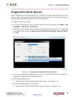
Page 22: ...t All Programs Tera Term Tera Term 2 In the New connection window configure the settings as shown in Figure 3 3 Select the serial COM port associated with Silicon Labs Dual CP210x USB to UART Bridge E...

Page 23: ...MHz Type 156 25 and press Enter c Choose Si5368 operating mode Select Free Run using XA XB crystal Type 2 and press Enter 7 Close the Tera Term Pro terminal program window Program the FPGA 1 Launch t...

Page 24: ...U1250 board by selecting the default value on each wizard page Click Next Next Next Finish c In the hardware view right click xcku040 and click Program Device Figure 3 6 d In the Bitstream file field...

Page 25: ...the reference design After programming each VIO core can be controlled in the Vivado IDE To add probes to each VIO window 1 Open the VIO dashboard On the top panel of the Vivado IDE click Window Dash...

Page 26: ...channel 0 through the training port of the 10 Gigabit Ethernet PCS PMA IP core hw_vio_4 1 stat_ch1_ Monitors the status vector signals of the 10 Gigabit Ethernet PCS PMA IP core for channel 1 hw_vio_3...

Page 27: ...a Advertise Channel 1 is KR capable Set value 0080 on ch1_an_adv_data_31_16 b Advertise Channel 1 supports FEC and is requesting FEC support from the partner Set value C000 on ch1_an_adv_data_47_32 c...

Page 28: ...ing done to 1 on channel 0 This indicates to the Training Algorithm that the LP transmitter has been successfully trained Set value 1 on ch0_training_done l Enable Training on channel 0 Set value 1 on...

Page 29: ...7 1 April 19 2017 www xilinx com Chapter 3 Bringing Up the Design Source the script in the Tcl console of the Vivado IDE as shown in Figure 3 10 X Ref Target Figure 3 10 Figure 3 10 Source enable_fec_...

Page 30: ...is complete an_complete and the 10GBASE KR is negotiated successfully in the stat_ch0 and stat_ch1 VIO windows Figure 3 11 It should take only a second or two for 10GBASE KR IP core to negotiate succ...

Page 31: ...ated with the Silicon Labs CP210x USB to UART Bridge Standard COM Port and click Connect Figure 3 13 to open the Ethernet Controller application for the 10GBASE KR TRD TIP The COM port associated with...

Page 32: ...t channel 0 and channel 1 are up and ready when the ETH0 PHY and ETH1 PHY indicators are green Figure 3 14 In the control panel for both channel 0 and channel 1 select Internal Generator and enter 150...

Page 33: ...entered are 46 bytes to 1 500 bytes TIP The relationship between payload size and throughput can be demonstrated by changing the payload size Reducing the payload size causes a dip in performance Ref...

Page 34: ...dropped Figure 3 16 4 Next select the Channel 1 Statistics tab and verify if any packets were in error or were dropped Figure 3 17 The TX MAC statistics for Channel 0 should match the RX MAC statisti...

Page 35: ...the USB to JTAG port U80 on the KCU1250 board The control computer periodically reads data samples via hw_axi_1 and creates an eye scan For more details refer to In System Eye Scan of a PCI Express L...

Page 36: ...er 3 Bringing Up the Design IMPORTANT Do not disconnect the USB to JTAG connection This connection is required for the control computer to interact with the JTAG to AXI Master IP core X Ref Target Fig...

Page 37: ...mes available after the run_eyescan tcl file is sourced To initiate a scan type run_eyescan in the Tcl console Figure 3 19 This command initiates Vertical and Horizontal sweeps Data sample collection...

Page 38: ...he GTH transceiver parallel data via VIO The unmodified file is located at working_directory kcu1250_10gbase_kr hardware vivado runs impl_run 10gbasekr_trd srcs sources_1 bd mac_phy ip mac_phy_ten_gig...

Page 39: ..._10gbasekr_trd ready_to_test fec_and_err_injection debug_nets ltx c Click Program Figure 3 21 There are seven VIO cores in the reference design After programming they can be controlled in the Vivado I...

Page 40: ...0 1 0 ch0_fec_corr_blocks Toggle 0 1 0 ch0_fec_uncorr_blocks Table 3 2 VIO Dashboard Mapping for the FEC and Error Injection BIT File VIO Dashboard Mapping Comments hw_vio_7 1 training_ _ch1 Configur...

Page 41: ...the insert_ _bit_error_ VIO window Set insert_multi_bit_rx_vector to h FFF This signal allows you to set the number of bits which are in error in succession A value of h FFF indicates a burst of 12 bi...

Page 42: ...1 For reads Set the training_addr_ch to a DRP address example h 00_007F TX_MARGIN_FULL_1 TX_MARGIN_FULL_0 Set the training_rnw_ch to 1 Toggle 0 1 0 enable_ch The read value will be available on train...

Page 43: ...Reference Design directory structure is described in Appendix A Directory Structure IMPORTANT The 10 Gigabit Ethernet MAC IP core 10G MAC requires a license to build the design Obtain the license at t...

Page 44: ...n it 1 Launch the Vivado Integrated Design Environment IDE and set up the reference design project In Windows 7 Click Start All Programs Xilinx Design Tools Vivado 2017 1 Vivado 2017 1 a In the Tcl co...

Page 45: ...s maximum allowed by Windows move the kcu1250_10gbasekr_trd directory directly under C 2 Select the Sources tab In the Hierarchy window two IP Integrator IPI block designs are referenced Figure 4 2 Bl...

Page 46: ...esigns The top level file also instantiates the VIO cores to configure and monitor the 10 Gigabit Ethernet PCS PMA IP core 3 In the Flow Navigator click Generate Bitstream 4 In the No Implementation R...

Page 47: ...ller in mac_phy bd 1 To generate the application ELF file to run on the MicroBlaze processor the block design must be exported and built in the SDK To launch SDK with the mac_phy block design exported...

Page 48: ...w xilinx com Chapter 4 Implementing and Simulating the Design 2 In the SDK window Figure 4 4 select File New Application Project to build an application X Ref Target Figure 4 4 Figure 4 4 Creating an...

Page 49: ...www xilinx com Chapter 4 Implementing and Simulating the Design 3 In the Application Project window Figure 4 5 enter the project name as kcu1250_10gbasekr_top and click Next X Ref Target Figure 4 5 Fi...

Page 50: ...58 v2017 1 April 19 2017 www xilinx com Chapter 4 Implementing and Simulating the Design 4 Select Empty Application and click Finish Figure 4 6 X Ref Target Figure 4 6 Figure 4 6 Select Empty Applicat...

Page 51: ...ter 4 Implementing and Simulating the Design 5 In the project explorer tab Figure 4 7 right click kcu1250_10gbasekr_top select Import and under the General tab select File System Click Next X Ref Targ...

Page 52: ...re source Select the source directory in the left pane and click Finish Figure 4 8 The application ELF file will be generated and available at working_dir kcu1250_10gbasekr_trd hardware vivado runs im...

Page 53: ...Controller in eyescan_sys bd 1 To generate the application ELF file to run on the MicroBlaze processor the design must be exported and built in the SDK To launch SDK with eyescan_sys block design exp...

Page 54: ...xilinx com Chapter 4 Implementing and Simulating the Design 2 In the SDK window Figure 4 10 select File New Application Project to build an application X Ref Target Figure 4 10 Figure 4 10 Building an...

Page 55: ...om Chapter 4 Implementing and Simulating the Design 3 In the Application Project window Figure 4 11 enter the project name as kcu1250_10gbasekr_eyescan and click Next X Ref Target Figure 4 11 Figure 4...

Page 56: ...v2017 1 April 19 2017 www xilinx com Chapter 4 Implementing and Simulating the Design 4 Select Empty Application and click Finish Figure 4 12 X Ref Target Figure 4 12 Figure 4 12 Selecting Empty Appli...

Page 57: ...4 Implementing and Simulating the Design 5 In the project explorer tab Figure 4 13 right click kcu1250_10gbasekr_eyescan select Import and under the General tab select File System Click Next X Ref Ta...

Page 58: ...escan Select the source_eyescan directory in the left pane and click Finish Figure 4 14 The application ELF file will be generated and available at working_dir kcu1250_10gbasekr_trd hardware vivado ru...

Page 59: ...scripts create_download_bit tcl The create_download_bit tcl script runs the update_mem command and combines kcu1250_10gbasekr_top bit kcu1250_10gbasekr_top elf and kcu1250_10gbasekr_eyescan elf into s...

Page 60: ...el 0 The test bench waits to receive the 10 packets on each channel without errors and then ends the simulation with a Simulation Passed message Simulating the AXI UART Lite IP and MicroBlaze processo...

Page 61: ...ation in Modelsim Questa 1 In the Flow Navigator under Simulation click Run Simulation Run Behavioral Simulation Figure 4 16 To run a simulation using the Vivado Design Suite Simulator 1 In the Flow N...

Page 62: ...lect Vivado Simulator in the Target simulator field and click Yes when asked if it is OK to change your target simulator to Vivado Simulator click OK in the Project Settings window 3 In the Flow Navig...

Page 63: ...ne CARD Backplane KCU1250 Board CHANNEL 1 CHANNEL 0 CHANNEL 1 CHANNEL 0 XCKU040 2FFGA1156C FPGA 64 bits XGMII 64 bits at 156 25MHz 10GBASE KR 64 bits at 156 25MHz AXI Interconnect AXI UART Lite MicroB...

Page 64: ...Core The 10 Gigabit Ethernet PCS PMA 10GBASE KR IP core provides an XGMII interface to connect to a 10 Gigabit Ethernet MAC IP core and implements a 10 3125 Gb s serial single channel PHY GTH transce...

Page 65: ...onitor block monitors the AXI4 Stream ports of the 10 Gigabit Ethernet MAC IP core and reports throughput The User Control and Status Register block passes information to and from the Ethernet Control...

Page 66: ...channel 0 48 h111100000000 For channel 1 48 h222200000000 XIL_MAC_ID_OTHER Parameter Destination MAC Address For channel 0 48 h222200000000 For channel 1 48 h111100000000 Clock and Reset Ports reset I...

Page 67: ...hin this block counts the clocks until one second has elapsed during which time counters have collected data about link performance Four counters collect information on the transactions on the AXI4 St...

Page 68: ...clk Input 156 25 MHz clock Transmit Ports on the AXI4 Stream Interface tx_axis_tdata 63 0 Input Data to be transmitted to the 10 Gigabit Ethernet MAC IP core tx_axis_tkeep 7 0 The transmit keep signal...

Page 69: ...last Input End of frame indicator on received packets Valid only along with asser tion of rx_axis_tvalid rx_axis_tvalid Input Source ready to provide data Indicates that the MAC is presenting valid da...

Page 70: ...m are MicroBlaze local memory Processor system reset MicroBlaze debug module AXI Interrupt controller In Vivado IPI adding the MicroBlaze IP core and running the connection automation creates the Micr...

Page 71: ...ontroller application to the AXI UART Lite to the MicroBlaze processor subsystem to other peripherals and back For more details on the MicroBlaze processor core see the MicroBlaze Soft Processor Core...

Page 72: ...and JTAG to AXI Master IP core The block RAM stores the data read from the DRP port of the transceiver For more details on the AXI Block RAM Controller IP see the AXI BRAM Controller website Ref 28 JT...

Page 73: ...ontroller The address map for the AXI slaves is shown in Figure 5 6 For more details on the AXI Interconnect see the AXI Interconnect website Ref 25 Clocking and Reset The 10 Gigabit Ethernet PCS PMA...

Page 74: ...et IP core in the processor system This reset also drives the eye scan system Another external reset dip switch drives the Channel 1 10 Gigabit Ethernet PCS PMA IP core the 10 Gigabit Ethernet MAC IP...

Page 75: ...CH0 PHY CH0 MAC CH0 Traffic Gen Mon CH1 PHY CH1 Traffic Gen Mon CH1 MAC reset ch0 reset_ch0_n Processor System Reset peripheral_aresetn AXI UART Lite AXI Interrupt Controller AXI Interconnect intercon...

Page 76: ...tes with the MicroBlaze Processor Server Application through a UART interface to control test parameters collect statistics and display current status of the design The GUI displays the following info...

Page 77: ...oard through the UART COM port exposed by the Silicon Labs UART driver All transmitted and received data adheres to a custom command model followed by the client and server Command Format The command...

Page 78: ...tual register offset in the server application Using different command numbers instead of the actual register values allows the GUI to remain constant in spite of changes in the hardware design or the...

Page 79: ...ite commands i e if a write command with a certain command number is used to update a register value the same command number can be used with a read command to retrieve the value MicroBlaze Processor...

Page 80: ...iver and communicates with the client application running on the control computer The main task of the server is to read write values from to the registers specified in the READ WRITE commands issued...

Page 81: ...initiates either AXI Read Write request to the register offset values identified 11 The Executor then sends an appropriate response to the client on control computer through the UART driver NOTE The...

Page 82: ...rectory structures for the 10GBASE KR TRD is shown in Figure A 1 X Ref Target Figure A 1 Figure A 1 Targeted Reference Design Directory Structure scripts uc1250_10gbasekr_trd ready_to_test source GUI...

Page 83: ...urces needed to generate a bitstream sources Contains subfolders that contain HDL files custom IP that is packaged VIO IP files constraint files and test bench files hdl Contains HDL files ip_packaged...

Page 84: ...miter 1 byte MAC destination address 6 bytes MAC source address 6 bytes Length Type field 2 bytes FCS 4 bytes This gives a total overhead of 38 bytes per Ethernet packet Table B 1 shows the effective...

Page 85: ...when read Each peripheral connected to the MicroBlaze processor subsystem is assigned an offset address which is the base address for that peripheral Figure 5 5 shows the addresses assigned to the Tr...

Page 86: ...ed Payload Byte Count Register 0x4AA0_000C Bit Position Mode Default Value Description 1 0 Read Only 00 Sample count Increments once every second 31 2 0 Receive payload byte count This field contains...

Page 87: ...Count Register 0x4AA1_0008 Bit Position Mode Default Value Description 1 0 Read Only 00 Sample count Increments once every second 31 2 0 Transmit packet count This field contains the count for the eve...

Page 88: ...ister 0x4AA1_0014 Bit Position Mode Default Value Description 0 Read or Write 0 Reserved 1 0 Enable generator if internal generator is selected 31 16 d 125 Ethernet frame Data payload size allowed val...

Page 89: ...ies and troubleshooting tips References The most up to date information for this design is available on these websites KCU1250 Characterization Kit KCU1250 Characterization Kit Documentation KCU1250 C...

Page 90: ...10 Gigabit Ethernet Media Access Controller 10GEMAC website 17 10 Gigabit Ethernet PCS PMA with FEC Auto Negotiation 10GBASE KR website 18 Vivado Design Suite User Guide Logic Simulation UG900 19 10G...

Page 91: ...produce modify distribute or publicly display the Materials without prior written consent Certain products are subject to the terms and conditions of Xilinx s limited warranty please refer to Xilinx s...

Reviews: