background image


WM_PRJ_Q2400_PTS_005 -007  


18th January 2006  


 Confidential©  

All rights reserved 


Page: 

19

 / 

51


This document is the sole and exclusive property of WAVECOM. Not to be 

distributed or divulged without prior written agreement. 


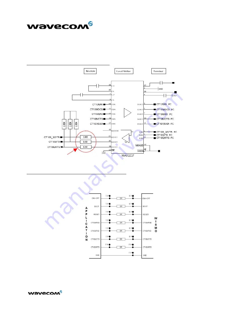
To enable the module to switch OFF correctly, the level shifter outputs (module 

side) or host processor outputs must be set at low level (0V) or in high 
impedance.  

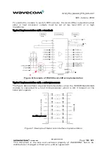
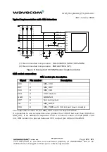
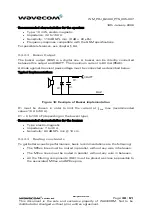
Typical implementation with a terminal: 


VCC 

+3V 

+3V 

+3V 

DCE DTE 


Figure 6: Example of RS232 level shifter implementation 

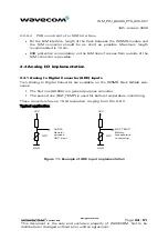
Typical implementation with a microprocessor: 

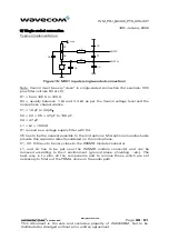
The figure above shows a typical implementation when the WISMO Quik Q24x6 

module is connected to a host microprocessor which is 2.8 V tolerant on the 

serial port signals. 

Host Microprocessor


Figure 7: Example of Serial Link interface implementation 

Summary of Contents for WISMO Quik Q2406

Page 1: ...WISMO Quik Q2400 series Q2406 and Q2426 Customer Design Guidelines Revision 007 Date January 2006...

Page 2: ...ument is the sole and exclusive property of WAVECOM Not to be distributed or divulged without prior written agreement WISMO Quik Q2400 series Q2406 and Q2426 Customer Design Guidelines Reference WM_PR...

Page 3: ...echanical information due to change of module design 003 26 Feb 05 Add SIM 1 8 3V management Update of 3V SIM Socket implementation diagram 004 26 Feb 05 No content modification document goes from ver...
Page 4: ...part references and suppliers 8 versions of the WISMO Quik Q24x6 sub series are available Q2406A E GSM GPRS 900 1800 MHz version with 16 Mbits of Flash memory and 2 Mbits of SRAM 16 2 Q2406B E GSM GPR...

Page 5: ...1 1 3 Additional customizing functions 10 1 1 4 RoHS compliance 10 2 Baseband Design 11 2 1 Power supply and ground design rules 11 2 1 1 Electrical constraints 11 2 1 2 Design Requirements 13 2 1 3 P...

Page 6: ...istics 38 3 2 Antenna implementation 38 3 2 1 Recommendations 38 3 2 2 RF connection 39 4 Mechanical specifications 41 5 PCB design 42 5 1 General design rules 42 5 2 Design rules for application manu...
Page 7: ...tion 24 Figure 12 Microphone decoupling capacitor 25 Figure 13 Example of main microphone MIC2 implementation differential connection 26 Figure 14 MIC1 inputs differential connection 27 Figure 15 MIC1...
Page 8: ...r its use Please read carefully the safety precautions for a terminal based on WISMO Quik Q24x6 Series General information about Wavecom and its range of products is available at the following interne...

Page 9: ...exclusive property of WAVECOM Not to be distributed or divulged without prior written agreement Reference documents 1 WISMO Quik Q2406 and q2426 Product Specification WM_PRJ_Q2400_PTS_002 2 WISMO Qui...

Page 10: ...der 3 6 Volts 1 Watt GSM1800 1900 radio section running under 3 6 Volts 1 1 1 3 Power supply voltage Digital section running under 2 8 Volts 3V only SIM interface for both 1 8 V and 5 V SIM interface...

Page 11: ...ce and Microphone Base connector Battery Antenna SIM connector 1 1 4 RoHS compliance The WISMO Quik Q24x6 sub series is now compliant with RoHS Restriction of Hazardous Substances in Electrical and El...

Page 12: ...he bursted emission in GSM GPRS the power supply must be able to deliver high current peaks in a short time and assured that the voltage delivered to the module remains always under the limits specifi...

Page 13: ...the total impedance battery contacts protections PCB should be 150 m to limit voltage drop out within emission burst As the radio power amplifier is directly connected to VBATT the module is sensitive...

Page 14: ...id any phase error Insufficient power supply voltage could dramatically affect some RF performances TX power of course and modulation spectrum EMC performances spurious emission Emissions spectrum Pha...

Page 15: ...nal impedance of the battery must be lower than 150 m to limit voltage drop out within emission burst max drop 0 3 V 2W Battery internal impedance must take into account the internal impedance of the...

Page 16: ...ear the module power supply could also be added refer to section 2 1 3 3 The routing must be done in such a way that the total impedance line must be 10 m 217 Hz This impedance must include the via im...

Page 17: ...better results In case a ferrite bead is used the recommendation given for the power supply connection must be carefully followed high current capacity and low impedance 2 2 Digital I O and periphera...

Page 18: ...h a standard 96 kHz interface The maximum speed transfer is 400 kbits s Note The two wire interface is reserved for future use A software emulated version of this interface using GPIOs is available Se...

Page 19: ...S Clear To Send output CT106 CTS Data Terminal Ready input CT108 2 DTR Data Set Ready output CT107 DSR Note the WISMO Quik Q24x6 module is a DCE Data Communication Equipment The Q24x6 sub series has b...

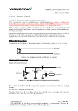
Page 20: ...side or host processor outputs must be set at low level 0V or in high impedance Typical implementation with a terminal VCC 3V 3V 3V DCE DTE R Figure 6 Example of RS232 level shifter implementation Ty...

Page 21: ...lue is determined by its input capacitance That explains why some combinations speed voltage are incompatible 2 2 6 SIM interface 2 2 6 1 SIM 3V management The SIM interface controls a 3 V SIM card on...

Page 22: ...LC208SC6 SGS THOMSON 2 Recommended components ESDA6V1SC6 ST Figure 8 Example of 3V SIM Socket implementation SIM socket connection SIM socket pin description Signal Pin number Description VCC 1 SIM_VC...

Page 23: ...As for 3 V SIM it is recommended to add Transient Voltage Suppressors on the signals connected to the SIM socket refer to Figure 9 Typical implementation CIN RIN DATA DDRV DVCC M2 M1 M0 CLK RST I O V...

Page 24: ...s for 3 V SIM it is recommended to add Transient Voltage Suppressors on the signals connected to the SIM socket refer to Figure 10 Typical implementation CIN RIN DATA DDRV DVCC M2 M1 M0 CLK RST I O VC...

Page 25: ...cm ESD protection is mandatory on the SIM lines if access from outside of the SIM connector is possible 2 3 Analog I O implementation 2 3 1 Analog to Digital Converter ADC inputs Two Analog to Digita...

Page 26: ...ral The MIC2 inputs already include the biasing for an electret microphone allowing an easy connection to a handset The MIC1 inputs do not include an internal bias MIC1 SPK1 is then appropriate for a...

Page 27: ...one MIC2 implementation differential connection C1 33 pF to 47 pF C2 C3 C4 47 pF to 100 pF L1 L2 100 nH C1 has to be the nearest possible to the microphone Microphone manufacturers provide this capaci...

Page 28: ...100 to 330 R2 R3 usually between 1 k and 3 3 k as per the microphone characteristics C1 33 pF to 47 pF C2 C3 C4 47 F to 100 pF C5 47 F L1 L2 100 nH R1 and R4 are used as a voltage supply filter with...

Page 29: ...0 R2 usually between 1 k and 3 3 k as per the VAUDIO voltage level and the microphone characteristics C1 10 pF to 33 pF C2 C3 C5 47 pF to 100 pF C4 47 F L1 L2 100 nH R1 is used as a voltage supply fil...

Page 30: ...as shielding in order to avoid any disturbance on the audio path Speaker outputs SPK2 are push pull amplifiers and can be loaded down to 150 and up to 1 nF These outputs are differential and the outp...

Page 31: ...rent is 80 mA PEAK A diode against transient peak voltage must be connected as described below Typical implementation C1 D1 VBATT BUZ R1 Figure 18 Example of Buzzer implementation R1 must be chosen in...

Page 32: ...X55 may cause damage to the battery This circuit uses an interface which consists of a current source inputs CHG_IN where the constant current has to flow in order to charge the battery This current v...

Page 33: ...to be chosen to have a RC filter with a time constant lower than 2 ms Calculation examples CTN 25 C 47 k CTN 55 C 10 k CTN 10 C 300 k CTN 10 C x VCC CTN 10 C R1 x BAT_TEMP full range R1 47 k BAT_TEMP...

Page 34: ...e Flash memory of the WISMO module The internal boot procedure is started when this pin is low during the reset of the module In normal mode this pin has to be left open In Internal boot mode low leve...

Page 35: ...external device It then behaves as an output If no external reset is necessary this input can be left open If used emergency reset it has to be driven by an open collector or an open drain output BOO...

Page 36: ...n Operating conditions Parameter Condition Min Max Unit Output voltage I 10 mA 2 74 2 86 V Output Current 10 mA 2 10 VCC_RTC Real Time Clock Supply 2 10 1 General VCC_RTC input is used to provide a ba...

Page 37: ...RTC Regulator 2 5 V 10 With very Low Iq VBATT 470 1K Ex 470uF Shottky Diode En Vout Gnd Vin Figure 22 RTC Supplied by a capacitor Estimated range with 470 F Capacitor 30 seconds 2 10 2 2 Super Capacit...

Page 38: ...gure 24 RTC supplied by a battery cell with regulator Estimated range with 2 mAh rechargeable battery 3 days Warning Before battery cell assembly insure that cell voltage is lower than 2 75V to avoid...

Page 39: ...at least Frequency depends on application A dual Band antenna shall work in all these frequency bands 3 2 Antenna implementation The impedance is 50 nominal and the DC impedance is 0 3 2 1 Recommendat...

Page 40: ...ble The coaxial cable shall not be placed close to devices operated at low frequencies Some signals like VBATT and charger line may require some EMI RFI decoupling parallel 33 pF capacitor close to th...

Page 41: ...r written agreement 3 Antenna cable preparation is shown in Figure 27 Figure 27 Antenna cable preparation drawing not to scale Note The WISMO Quik Q24x6 sub series does not include any antenna switch...

Page 42: ...dule to be soldered on the Ground plane see Wavecom recommendation for lead free soldering in Section 5 3 Figure 28 gives the overall dimension of the module taking into account the PCB dimension and...

Page 43: ...ground line on the PCB It is recommended to protect clock signals with a ground belt Refer to the following sections for other constraints 2 1 3 for the Power Supply 2 2 6 4 for the SIM interface 2 3...

Page 44: ...18th January 2006 Confidential All rights reserved Page 43 51 This document is the sole and exclusive property of WAVECOM Not to be distributed or divulged without prior written agreement 5 5 Pads des...

Page 45: ...ted by the application to the RF receiver in the receiver band ESD protection on SIM if accessible from outside serial link etc Refer to section 2 2 6 SIM interface Length of the SIM interface lines p...

Page 46: ...he standard Xmodem protocol Therefore the application shall either allow a direct access to the WISMO serial link through an external connector or implement any mechanism allowing the WISMO firmware t...

Page 47: ...connected to the serial bus of the modem The necessary signals to proceed with the downloading are Rx Tx RTS CTS and GND Prior to running the WAVECOM downloader the modem has to be set in download mo...

Page 48: ...RESET and GND Prior to running the Wavecom downloader the module has to be set in download mode For this the BOOT signal has to be set to low while powering ON or resetting the modem Typical implemen...

Page 49: ...cument is the sole and exclusive property of WAVECOM Not to be distributed or divulged without prior written agreement CT103 TXD GPIO_SCL GPIO_SDA CT106 CTS CT108 2 DTR CT104 RXD CT105 RTS NC_BOOT NC_...

Page 50: ...8th January 2006 Confidential All rights reserved Page 49 51 This document is the sole and exclusive property of WAVECOM Not to be distributed or divulged without prior written agreement Figure 32 Dow...

Page 51: ...he following reference 14 5087 060 930 861 The matting connector has the following reference 24 5087 060 X00 861 with X 2 or 9 The stacking height is 3 0 mm For further details see GPC data sheets in...

Page 52: ...written agreement 9 4 Speaker Possible suppliers SANYO HOSIDEN PRIMO PHILIPS 9 5 Antenna Cable The following cable reference has been qualified for being mounted on WISMO Quik Q24x6 sub series RG178 9...

Page 53: ...France Tel 33 0 1 46 29 08 00 Fax 33 0 1 46 29 08 08 Wavecom Inc 4810 Eastgate Mall Second Floor San Diego CA 92121 USA Tel 1 858 362 0101 Fax 1 858 558 5485 WAVECOM Asia Pacific Ltd 4 F Shui On Cent...

Reviews: