


500-003124-000
4-7
recommended.
When accessing the Data Registers as bytes, it is possible for the
value in the Data Register to be updated
between
byte reads, potentially scrambling
the data. Section 4.5 provides methods to avoid scrambled byte data reads.
The data is a linear binary representation of the input voltage on the
corresponding channel at the time of the most recent conversion. The LSB weight (that
is, the voltage value corresponding to a single bit of data) depends on the input voltage
range, which in turn depends on the range and gain jumper configuration (see Section
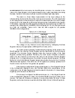
5 for details). Calculate the LSB weight by dividing the full-scale range by 4096. For
example, the LSB weight for a VMIVME-3124 configured for
10 V at unity gain would
be 4.883 mV (20/4096). Table 4.2.5-1 lists the LSB weights for all possible
VMIVME-3124 configurations.
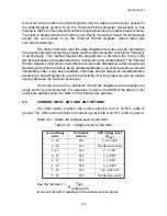
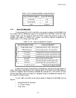
Table 4.2.5-1 LSB Weight
LSB Weight
Voltage Range
Gain x1
Gain x10
Gain x100
5 V
2.441 mV
.2441 mV
24.41
V
10 V
4.883 mV
.4883 mV
48.83
V
0-10 V
2.441 mV
.2441 mV
24.41
V
The voltage on any channel can be determined by multiplying the Data
Register value by the appropriate LSB Weight from Table 4.2.5-1.
Two other values necessary to determine the meaning of the values in the
Data Registers: the Channel Pointer Register and the Max Buffer bit, both previously
described. The Channel Pointer Register holds the channel number of the Data
Register currently being updated. Therefore, the most recent complete conversion
data is for the channel one less than the value of the Channel Pointer Register
(modulo 32 or 16, depending upon the number of active Data Registers). The Max
Buffer bit in the Control/Status Register determines whether there are 16 or 32 active
differential data registers. If the bit is set, all 32 registers are actively updated, but if
the bit is clear, only the first 16 registers are updated.
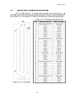
If the board is configured for single-ended inputs (i.e. if the Single-Ended bit
in the Configuration Register is set), then the Max Buffer bit is meaningless. In this
configuration, the 32 Data Registers contain the data for channels 0-31 consecutively,
beginning with channel 0 at offset $40.
If the board is configured for differential inputs (i.e., if the Single-Ended bit
in the Configuration Register is clear), then the Max Buffer bit may be either set or
cleared. The trade-off is between simplicity of access (Max Buffer bit clear; 16 Data
Registers) and relaxed access requirements (Max Buffer bit set; 32 Data Registers).


