Physical Details
EBX-37 Reference Manual
12
Figure 5. VL-CBR-4004 Dimensions and Mounting Holes
(Not to scale. All dimensions in inches.)
J1 J2 J3 J4
J6 J7 J8 J9
J5
+
2.38
2.87
0.25
0.40
1.95
0.70
0.63
0.62
0.06
Page 1: ...Reference Manual DOC REV 5 25 2017 VL EBX 37 Mamba Intel Core 2 Duo SBC with Video Ethernet USB Serial SATA Audio Analog Digital I O PCIe Mini Card eUSB and SPX...
Page 2: ...very effort has been made to ensure this document is error free VersaLogic makes no representations or warranties with respect to this product and specifically disclaims any implied warranties of merc...
Page 3: ...vision 6 5 102 release Support Page The following resources are available for the VL EBX 37 Reference Manual PDF format Data sheet VersaAPI Installation and Reference Guide This is a private page for...
Page 4: ...on 7 Basic Setup 7 CMOS Setup 9 Operating System Installation 9 Physical Details 10 Dimensions and Mounting 10 Hardware Assembly 13 Standoff Locations 13 External Connectors 14 VL EBX 37 Connector Loc...
Page 5: ...SVGA Output Connector J11 27 LVDS Flat Panel Display Connector J31 J33 28 Compatible LVDS Panel Displays 29 Console Redirection 29 Ethernet Interface J12 J15 30 Ethernet Connectors 30 Status LED J5 3...
Page 6: ...rrupts 54 On board I O Devices 55 Special Registers 56 PLED and Product Code Register 56 PLD Revision and Type Register 57 Special Control Register 58 Appendix A References 59 Appendix B Custom Progra...
Page 7: ...ible PS 2 keyboard and mouse support PC 104 Plus PCI ISA expansion TVS devices for ESD protection CPU temperature sensor EBX standard 5 75 x 8 00 footprint Field upgradeable BIOS with OEM enhancements...
Page 8: ...24 bits Up to 64 MB shared DRAM pre allocated plus up to 1700 MB using Intel DVMT SATA Interface Two SATA 3 Gb s ports Flash Interface USB SSD interface eUSB PCIe Mini Card socket Ethernet Interface T...
Page 9: ...Introduction EBX 37 Reference Manual 3 VL EBX 37 Block Diagram Figure 1 VL EBX 37 Block Diagram...
Page 10: ...ir To reliably function at extreme temperatures the extended temperature model specifications deviate from the standard model in the following ways The DRAM interface is slowed PC3 6400 memory runs at...
Page 11: ...ct with the bottom side of the VL EBX 37 LITHIUM BATTERY Warning To prevent shorting premature failure or damage to the lithium battery do not place the board on a conductive surface such as metal bla...
Page 12: ...e of your company your phone number and e mail address The name of a technician or engineer that can be contacted if any questions arise Quantity of items being returned The model and serial number ba...
Page 13: ...ng steps outline the procedure for setting up a typical development system The VL EBX 37 should be handled at an ESD workstation or while wearing a grounded antistatic wrist strap Before you begin unp...
Page 14: ...R 201x into socket J31 on the bottom of the board Attach the adapter cable to the LVDS display On models A and F socket J33 can alternately be used Plug the USB CD ROM drive keyboard and mouse into on...
Page 15: ...D ROM drive and select to boot from the CD ROM drive 7 Install Operating System Install the operating system according to the instructions provided by the OS manufacturer See Operating System Installa...
Page 16: ...andards which provide for specific mounting hole and PC 104 Plus stack locations as shown in the diagram below Figure 3 VL EBX 37 Dimensions and Mounting Holes Not to scale All dimensions in inches 3...
Page 17: ...ent excessive flexing when expansion modules are mated and de mated Flex damage caused by excessive force on an improperly mounted circuit board is not covered under the product warranty Figure 4 VL C...
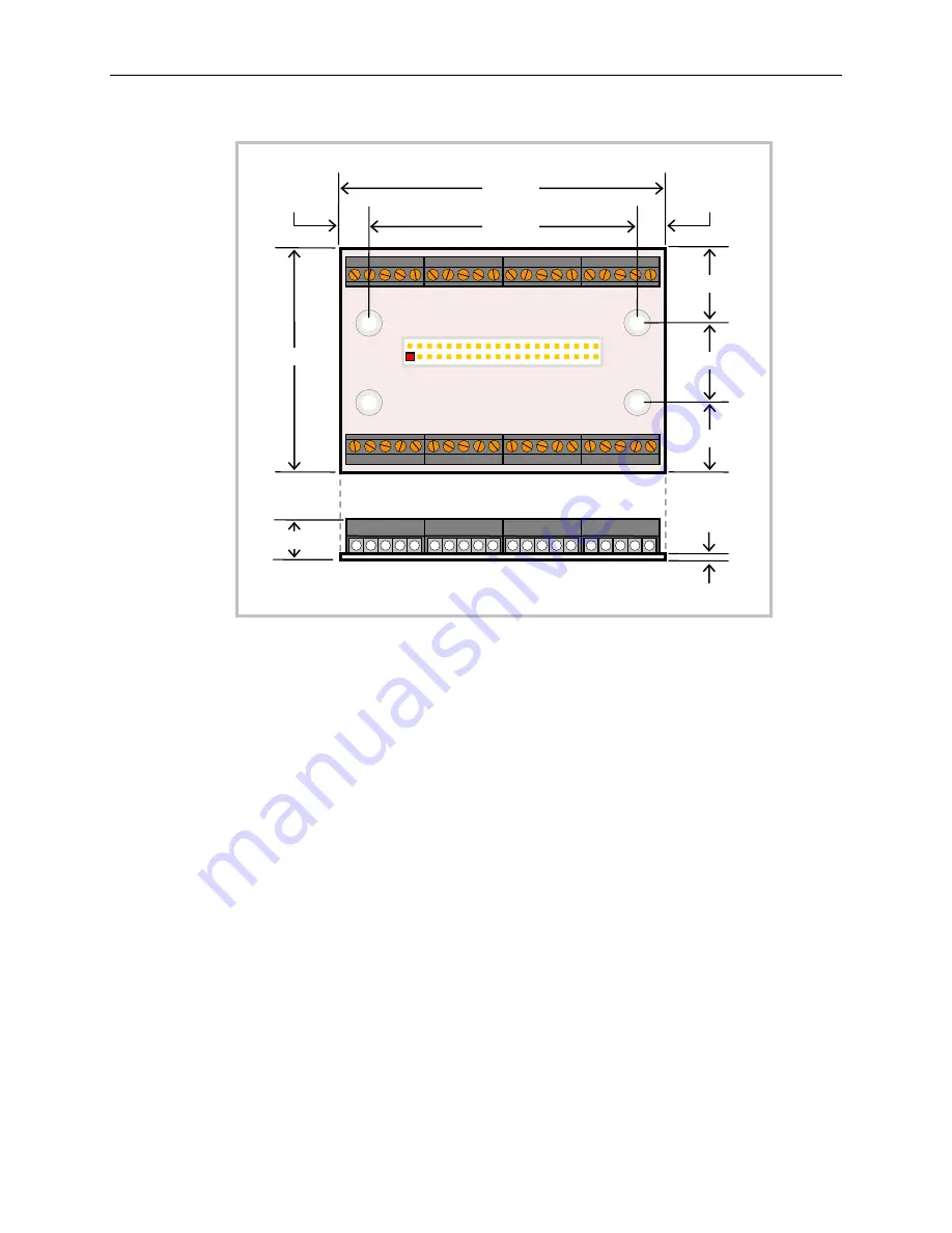
Page 18: ...cal Details EBX 37 Reference Manual 12 Figure 5 VL CBR 4004 Dimensions and Mounting Holes Not to scale All dimensions in inches J1 J2 J3 J4 J6 J7 J8 J9 J5 2 38 2 87 0 25 0 25 0 40 1 95 0 70 0 63 0 62...
Page 19: ...also serve as mounting struts for the PC 104 stack The entire assembly can sit on a table top or be secured to a base plate When bolting the unit down make sure to secure all eight standoffs A and B t...
Page 20: ...CI J20 21 ISA Battery J6 Power J12 Ethernet J4 J10 USB5 USB4 J3 J9 USB2 USB3 J2 J8 USB0 USB1 J1 J7 SATA1 SATA0 J18 User I O J17 Digital I O J22 Analog I O Timers J23 SPX Intel ICH9M Intel GM45 Intel C...
Page 21: ...ical Details EBX 37 Reference Manual 15 VL EBX 37 CONNECTOR LOCATIONS BOTTOM Figure 8 VL EBX 37 Connector Locations Bottom J29 SO DIMM 2 DDR3 J31 LVDS J27 eUSB Pin 1 J33 Dual Link High Res LVDS Models...
Page 22: ...rd 0 622 3 423 32 J15 Gigabit Ethernet 2 RJ45 1 632 7 280 30 J16 PC 104 Plus AMP 1375799 1 2 112 3 100 33 J17 Digital I O 1 32 FCI 89361 340LF VL CBR 4004A 12 2 mm 40 pin to 40 pin IDC to VL CBR 4004...
Page 23: ...utton Reset Conta Clip 10250 4 5 pin screw terminal J3 COM1 COM2 Kycon K42 E9P P A4N Dual stacked DB 9 male J4 PS 2 Keyboard and Mouse Kycon KMDG 6S 6S S4N Dual stacked PS 2 female J5 COM4 Conta Clip...
Page 24: ...8 VL CBR 4004 CONNECTOR LOCATIONS Figure 10 VL CBR 4004 Connectors The VL CBR 4004 can be attached to connector J7 digital I O and connector J22 analog I O and timers 2 1 40 39 J1 J2 J3 J4 J6 J7 J8 J9...
Page 25: ...l 2 3 In Erase CMOS RAM and real time clock 1 2 In 22 V2 System BIOS Selector In Backup system BIOS selected Out Primary system BIOS selected The Primary system BIOS is field upgradeable using the BIO...
Page 26: ...Input 10 GND Ground Note The 3 3VDC 12VDC and 12VDC inputs on the main power connector are only required for PC 104 Plus and PC 104 expansion modules that require these voltages POWER REQUIREMENTS The...
Page 27: ...xceed 18 Avoid using any additional connectors in the power delivery system The power and ground leads should be twisted together or as close together as possible to reduce lead inductance A separate...
Page 28: ...or 64 bit versions depending on the processor of the target system on which it will be executing Due to the way that this board maps memory 32 bit OS versions will not be able to identify or use more...
Page 29: ...tory Defaults and Restart on the Exit tab but CMOS restoration will continue to use custom defaults as long as they are available To remove custom defaults either re program the BIOS or follow the Sav...
Page 30: ...rdware monitor which includes a 16 bit fan tachometer register that can be read to obtain the speed of the fan on the VL EBX 37 When one byte of the 16 bit register is read the other byte latches the...
Page 31: ...to 16 bit address Bdata Bindex 1 Start Hardware Monitoring outp Bindex RLSREG Index Ready Lock Start Reg outp Bdata inp Bdata START Set bit 0 to start while keypressed ESC if kbhit keypressed getch R...
Page 32: ...ctors If the power supply you are using does not provide SATA connectors adapters are available Table 5 SATA Port Pinout J1 or J7 Pin Signal Name Function 1 GND Ground 2 TX Transmit 3 TX Transmit 4 GN...
Page 33: ...re It supports two types of video output SVGA and LVDS Flat Panel Display SVGA OUTPUT CONNECTOR J11 An adapter cable part number VL CBR 1201 is available to translate J11 into a standard 15 pin D Sub...
Page 34: ...Table 7 LVDS Flat Panel Display Pinouts J31 Pin J31 Signal Name J31 Function J33 Pin J33 Signal Name J33 Function 1 GND Ground 1 GND Ground 2 NC Not Connected 2 NC Not Connected 3 LVDSA3 Diff Data 3 3...
Page 35: ...ommunications port CMOS Setup and some operating systems such as DOS can use this console for user interaction Console redirection settings are configured on the Features tab of CMOS Setup The default...
Page 36: ...hese interfaces are protected against ESD damage ETHERNET CONNECTORS Two board mounted RJ45 connectors are provided to make connection with Category 5 or 6 Ethernet cables The 82574IT Ethernet control...
Page 37: ...hernet 1 7 ORN2 Orange LED Ethernet 1 8 GRN2 Green LED Ethernet 1 9 GND Ground 10 W_DISABLE PCIe Mini Card Disable W_Disable Signal The W_DISABLE is for use with optional wireless PCIe Mini Cards The...
Page 38: ...ame Function 1 WAKE Wake 2 3 3VAUX 3 3V auxiliary source 3 NC Not connected 4 GND Ground 5 NC Not connected 6 1 5V 1 5V power 7 CLKREQ Reference clock request 8 NC Not connected 9 GND Ground 10 NC Not...
Page 39: ...wing I O ranges are available to the ISA bus 019h 01Eh 022h 023h 026h 027h 02Ah 02Bh 032h 033h 036h 037h 03Ah 03Bh 03Eh 03Fh 043h 04Dh 053h 05Fh 063h 065h 067h 070h 078h 07Fh 0A2h 0A3h 0A6h 0A7h 0AAh...
Page 40: ...VL CBR 4004 Pin Silkscreen 1 Digital I O 1 J1 5 IO1 2 Digital I O 2 4 IO2 3 Digital I O 3 3 IO3 4 Digital I O 4 2 IO4 5 Ground 1 GND1 6 Digital I O 5 J2 5 IO5 7 Digital I O 6 4 IO6 8 Digital I O 7 3...
Page 41: ...is the default setting CA0h MOV DX CA8h MOV AL 26h SPICONTROL SPI Mode 00 24bit auto SPI 6 OUT DX AL MOV DX CA9h MOV AL 30h SPISTATUS 8MHz no IRQ left shift OUT DX AL MOV DX CABh MOV AL 08h SPIDATA1...
Page 42: ...MHz no IRQ left shift OUT DX AL MOV DX CABh MOV AL 44h SPIDATA1 Mirror Open Drain interrupts OUT DX AL MOV DX CACh MOV AL 0Ah SPIDATA2 MCP23S17 address 0x0A OUT DX AL MOV DX CADh MOV AL 40h SPIDATA3 M...
Page 43: ...e command OUT DX AL CALL BUSY Poll busy flag to wait for SPI transaction Write 55h to MCP23S17 register GPIOA MOV DX CABh MOV AL 55h SPIDATA1 data to write OUT DX AL MOV DX CACh MOV AL 14h SPIDATA2 MC...
Page 44: ...7 IRQSEL1 0 IRQ Select IRQ3 D6 IRQSEL0 0 D5 SPICLK1 1 SPI SCLK Frequency 8 333 MHz D4 SPICLK0 1 D3 HW_IRQ_EN 0 Hardware IRQ Enable Disabled D2 LSBIT_1ST 0 SPI Shift Direction Left Shifted D1 0 0 This...
Page 45: ...DIRECTION OF DIO LINES D15 D8 AS INPUTS Direction All Inputs OUT SPIDATA1 HFF MCP23S17 IODIRA Register Address OUT SPIDATA2 H0 MCP23S17 SPI Control Byte Write OUT SPIDATA3 H40 WHILE INP SPISTATUS AND...
Page 46: ...1 Ground Ground 3 Top DB9 2 Receive Data 27 5 RTS TxD 4 7 Request to Send 28 4 TXD TxD 5 3 Transmit Data 29 Ground Ground 6 8 Clear to Send 30 2 RXD RxD 7 4 Data Terminal Ready 31 3 CTS RxD 8 9 Ring I...
Page 47: ...he termination resistor should be enabled for RS 422 and the RS 485 endpoint station It should be disabled for RS 232 and the RS 485 intermediate station If RS 485 mode is used the half duplex differe...
Page 48: ...ectors are protected against ESD damage Table 14 COM1 2 Pinout VL CBR 5009 Connector J3 COM1 COM2 Top DB 9 J3 Pin Bottom DB 9 J3 Pin RS 232 1 1 DCD 2 2 RXD 3 3 TXD 4 4 DTR 5 5 Ground 6 6 DSR 7 7 RTS 8...
Page 49: ...3 GND Ground 4 MKPWR 5V Protected 5 KBCLK Keyboard Clock 6 No Connection Programmable LED J18 Connector J18 includes an output signal for attaching a software controlled LED Connect the cathode of th...
Page 50: ...and odd analog channels for example inputs 1 and 2 can also be combined as differential inputs The converter has a 100 kilo samples per second Ksps sampling rate with a 4 s acquisition time with per...
Page 51: ...nformation on custom orders ANALOG INPUT USING THE SPI INTERFACE See SPI Registers for a description of the SPI interface and registers Initiating an Analog Conversion Using the SPI Interface The foll...
Page 52: ...egister I O address CAFh to start a conversion 7 Poll the the ADCBUSY0 Bit 2 of the FPGA ADC DAC control status register I O address CAFh until this bit is a 0 not busy to indicate a conversion is com...
Page 53: ...ion on custom orders Analog Output Using the SPI Interface The following procedure can be used to set an analog output using the SPI interface 1 Write 27h to the SPICONTROL register I O address CA8h T...
Page 54: ...Timer 3 Clock Input 3 IO27 34 Output OCTC4 Timer 4 Counter Output 4 I028 36 Input GCTC4 Timer 4 Gate Input J9 1 IO29 37 Input ICTC4 Timer 4 Clock Input 2 IO30 38 Output OCTC5 Timer 5 Counter Output 3...
Page 55: ...nly by the permanent Master device on board The others are Data In and Data Out with respect to the Master The SPX implementation adds additional features such as chip selects and an interrupt input t...
Page 56: ...and auto slave select modes SPILEN1 SPILEN0 Frame Length 0 0 8 bit 0 1 16 bit 1 0 24 bit 1 1 32 bit D3 MAN_SS SPI Manual Slave Select Mode This bit determines whether the slave select lines are contro...
Page 57: ...QSEL by an SPI device 0 SPI IRQ disabled default 1 SPI IRQ enabled Note The selected IRQ is shared with PC 104 ISA bus devices CMOS settings must be configured for the desired ISA IRQ D2 LSBIT_1ST SPI...
Page 58: ...he SPI data word for example the LSB of a 24 bit frame would be SPIDATA1 Data is sent according to the LSBIT_1ST setting When LSBIT_1ST 0 the MSbit of SPIDATA3 is sent first and received data will be...
Page 59: ...t J26 Pin Signal Name Function 1 LINE_OUTR Line Out Right 2 Ground Ground 3 LINE_OUTL Line Out Left 4 Ground Ground 5 LINE_INR Line In Right 6 Ground Ground 7 LINE_INL Line In Left 8 Ground Ground eUS...
Page 60: ...dled through CMOS Setup Table 24 VL EBX 37 IRQ Settings default setting allowed setting Source IRQ 0 1 2 3 4 5 6 7 8 9 10 11 12 13 14 15 Timer 0 Keyboard Slave PIC COM1 COM2 COM3 COM4 Floppy RTC Mouse...
Page 61: ...I O Devices I O Device Standard I O Addresses PLED and Product ID Register CA0h Revision Indicator Register CA1h BIOS and Jumper Status Register CA2h Interrupt Control Register CA3h Interrupt Status...
Page 62: ...gister Bit Assignments Bit Mnemonic Description D7 PLED Light Emitting Diode Controls the programmable LED on connector J18 0 Turns LED off 1 Turns LED on D6 D0 PC Product Code These bits are hard cod...
Page 63: ...PLD code revision PLD4 PLD3 PLD2 PLD1 PLD0 Revision 0 0 0 0 0 Rev 0 1x These bits are read only D2 TEMP Temperature Rating This bit indicates whether the VL EBX 37 is rated for standard or extended te...
Page 64: ...he status of the system BIOS selector jumper at V2 1 2 0 Jumper installed backup system BIOS selected 1 No jumper installed primary system BIOS selected This bit is read only D6 BIOS_OR BIOS Jumper Ov...
Page 65: ...asheet Chipset Intel GM45 Intel ICH9 Intel GM45 Datasheet Intel ICH9 Datasheet Super I O Chip SMSC SCH3114 SCH3114 Datasheet Ethernet Controller Intel 82574IT Ethernet Controller Intel 8257IT Datashee...
Page 66: ...1 Enable interrupt D6 D5 IRQSEL 2 0 Specifies the interrupt mapping this setting is ignored when IRQEN 0 interrupts are disabled 000 IRQ3 default 001 IRQ4 010 IRQ5 011 IRQ10 100 IRQ6 101 IRQ7 110 IRQ...
Page 67: ..._TC4 Status for the 8254 Timer 4 output terminal count Interrupt when read 0 Timer output terminal count has not transitioned from 0 to a 1 level 1 Timer output terminal count has transitioned from a...
Page 68: ...mer 4 input clock is from User I O connector Input ICTC4 1 Timer 4 input clock is 4 16625 MHz internal clock PCI clock divided by 8 D2 TM3SEL Configure the clock source for 8254 Timer 3 0 Timer 3 inpu...
Page 69: ...J22 The internal clock is the PCI clock divided by 8 33 33 MHz 8 4 167 MHz ICTC3 can only be used with Timer 3 ICTC4 can only be used with Timer 4 The clock for Timer 5 is always the internal clock ex...
Page 70: ...MBASE13 TIMBASE12 TIMBASE11 TIMBASE10 TIMBASE9 TIMBASE8 Table 33 8254 Timer Base MS Address Register Bit Assignments Bit Mnemonic Description D7 D0 TIMBASE 15 8 Most significant 8 bits of the 16 bit T...
Page 71: ...riting a 0 is ignored D3 Reserved This bit is reserved Only write 0 to this bit and ignore read values D2 ADCBUSY0 This read only status bit returns the A D conversion status 0 A D is not busy doing a...