DNA/DNR-429-512/566 ARINC 429 Layer
Chapter 1
10
Introduction
Tel: 508-921-4600
www.ueidaq.com
Vers:
4.5
Date: December 2013
DNx-429-Chap1x.fm
© Copyright 2013
United Electronic Industries, Inc.
For the parity bit above, transmission and reception have different behaviors:
•
Transmit: parity can be selected to be Odd, Even, or None.
Selecting Odd/Even enables parity bit insertion into transmitter data bit
32. The parity generator counts the ONES in the 31-bit word. If Odd is
selected, the 32nd bit transmitted will make parity odd. If Even is
selected, the parity is even. The parity bit is automatically set and you
can't "force" it when sending a label. If None is selected, data is inserted
on bit 32 (taking whatever bit 32 you supply).
•
Receive: parity bit is is calculated by the chip, the value from the bus is
not used. The receiver parity circuit counts 1’s received, including the
parity bit, ARINC bit 32. If the result is odd, then "0" will appear in bit 32.
When receiving, the received parity bit is matched against the expected
value. If the received data is correct and parity is even, then the parity bit
should be 1 in the received word; if it is 0 it is a parity error. If the parity
is odd it should be 0; and error is 1. If the parity is disabled it sets zero or
one (depending on calculations) and you need to re-calculate parity for
bits 1-31 to deduce the actual value of the transmitted parity bit.
1.6.2
Receiver
Block
As indicated in
Figure 1-2
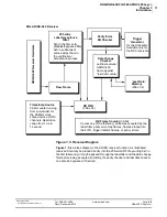
on page 6, the RX0 receiver in each Building Block
has a software-selectable label acceptance filter that accepts or rejects
incoming data words. As an option, you can choose to accept only “changed
data”. This option uses the “last received data” memory and places only
“changed” data into the receive FIFO. Unchanged data is discarded. The RX
FIFO can store up to 256 last received ARINC-429 32-bit frames, if
timestamping is not selected. If timestamping is selected, the RX FIFO is limited
to 128 frames and 128 timestamps. If the label filter is not selected, data is
placed directly into the 256-word FIFO.
Each building block shares communication configuration settings. This means
that the RX0, RX6, and TX0 of Building Block 1 share speed settings. Thus on
the 429-512 the pair of receivers (RX0 and RX6) will use the same speed. The
429-566 RX0 and TX0 channel also uses the same speeds.
The receivers are electrically connected in different ways on the 429-512 and
566. On the 429-512 board each of the two receivers is individually addressable.
If the board is a -566 version, however, (one receiver and one transmitter per
channel), the second receiver is used as a loopback controller for the associated
transmitter. To make the Loopback Connection between a TX1 and its
associated loopback RX1 on the -566 version, you must set up a port on the
channel.


