DNA/DNR-429-512/566 ARINC 429 Layer
Chapter 1
6
Introduction
Tel: 508-921-4600
www.ueidaq.com
Vers:
4.5
Date: December 2013
DNx-429-Chap1x.fm
© Copyright 2013
United Electronic Industries, Inc.
1.6
Device
Architecture
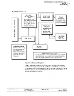
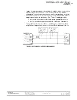
The DNx-429-512/566 Layer has 6 parallel ARINC processors running at
66MHz. Sub-processor DSPs run inside each ARINC processor. A block
diagram of the board is shown in
Figure 1-2
.
Figure 1-2. DNA/DNR-429-512/566 Logic Block Diagram
As shown in the diagram above, each RX/TX block contains two ARINC
Receivers and one ARINC Transmitter. The ARINC Receiver/Transmitter and
communication protocol functions are handled by Holt
(www.holtic.com)
HI-3282 serial transmitter/dual receiver chips (for both the 429-512 and -566)
and associated HI-8585 line drivers (for the 429-566 output only).
Filter bypass
Speed selector, error reporting, etc.
TX0 channel FPGA/DSP block
Speed selector, error reporting, etc.
TX Por
t
Ac
cess C
ontroller
RX0 channel FPGA/DSP block
2RX/1TX ARINC-429 transceiver protocol controllers (FPGA/DSP control/access Block 0)
SDI Filter
Label
Acceptance
Filter
RX FIFO
with
Timestamp
ARINC-429 (RX/TX Block 1)
ARINC-429 (RX/TX Block 2)
ARINC-429 (RX/TX Block 3)
ARINC-429 (RX/TX Block 4)
ARINC-429 (RX/TX Block 5)
RX6 channel FPGA/DSP block
data
data
data
control
control
control
status
status
status
ARI
N
C 429
Re
ce
iv
er
R
X
0
A
R
INC 429
T
ransmit
ter TX
0
ARI
N
C
42
9
R
ec
eiver RX1
Scheduler
Timebases(2)
FIFO
Timebase
256 x 25
Entries
Scheduler
Commands
256 x 32
Entries
Scheduler
Data
256 x 32
TX FIFO
Low Priority
Bypass Data
High Priority
Bypass Data
ARINC Pro
tocol
Con
tro
ller
S
ta
nda
rd DNA CL
I
– in 2RX configuration, RX6 is same as RX0
– in 1RX/1TX configuration, RX6 is used for loopback control
of TX0 channel
Trigger
Input 0
Output 0
Input 6
loopback
NOTE
: Block 0 has 3 ports: TX0, RX0, RX6
Block 1 has 3 ports: TX1, RX1, RX7
Block 2 has 3 ports: TX2, RX2, RX8
Block 3 has 3 ports: TX3, RX3, RX9
Block 4 has 3 ports: TX4, RX4, RX10
Block 5 has 3 ports: TX5, RX5, RX11


