


Electronic System
- 48 -
Pin
9,11,13,15:
GND
Pin
10,12,14,16:
DC
+12V
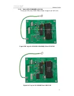
CN2--- From Main CPU PCB
Pin
1:
GND
Pin 2:
DC +5V
Pin 3-6:
Control wavelength step motor
Pin 7-10:
Control filter step motor
Pin 11-14:
Control lamp Change step motor
J4---
To lamp Change step motor
Pin 1-4:
Drive slit step motor
Pin
5: DC
+12V
J5---
To filter step motor
Pin 1-4:
Drive filter step motor
Pin
5: DC
+12V
J6---
To wavelength step motor
Pin 1-4:
Drive wavelength step motor
Pin
5: DC
+12V
J7---
To slit step motor
Pin 1-4:
Drive slit step motor
Pin
5: DC
+12V
J9---To filter Photo-coupler
Pin
1: GND
Pin 2:
DC +5V (0V). 0V: only at initiative position
Pin
3: DC
+1.2V
J11---To slit Photo-coupler
Pin
1: GND
Pin 2:
DC 0V (+5V). +5V: only at initiative position
Pin
3: DC
+1.2V
J12---To lamp limit switch
Pin
1: GND
Pin 2:
DC +5V (0V). 0V: only at initiative position
Pin
3: DC
+5V
J14---To wavelength Photo-coupler and limit switch
Pin
1: GND
Pin 2:
DC 0V (+5V). +5V: when the mobile block at start or
end point
Pin
3: DC
+5V
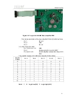
5.2.3 Transferring
PCB(In
Upper
Case)(SST8.417.100)
The layout of the Transferring PCB(In Upper Case) is shown in figure
5.17
Summary of Contents for SQ Series
Page 5: ......
Page 8: ...Introduction 3 Figure 1 5 Model UV 4802...
Page 12: ...Layout 7 Figure 3 2 Layout of UV 2800 Inside Bottom View...
Page 13: ...Layout 8 39 40 41 42 43 Figure 3 3 Layout of UV 2800 Top View...
Page 14: ...Layout 9 230V 44 45 46 47 48 49 50 51 Figure 3 4 Layout of UV 2800 Back View...
Page 18: ...Layout 13 Figure 3 7 Layout of UV 2802 S UV 2802PC S Inside Bottom View...
Page 19: ...Layout 14 43 44 45 46 47 Figure 3 8 Layout of UV 2802 S Top View...
Page 20: ...Layout 15 230V Figure 3 9 Layout of UV 2802 S UV 2802PC S Back View...
Page 23: ...Layout 18 Figure 3 11 Layout of UV 3802 Inside Bottom View...
Page 24: ...Layout 19 44 45 46 47 48 Figure 3 12 Layout of UV 3802 Top View...
Page 25: ...Layout 20 230V Figure 3 13 Layout of UV 3802 Back View...
Page 28: ...Layout 23 Figure 3 14 Layout of UV 4802 Inside Top View...
Page 29: ...Layout 24 Figure 3 15 Layout of UV 4802 Inside Bottom View...
Page 30: ...Layout 25 43 44 45 46 47 Figure 3 16 Layout of UV 4802 Top View...
Page 31: ...Layout 26 230V Figure 3 17 Layout of UV 4802 Back View...
Page 35: ...Optical 30 Figure 4 3 Optical System schematic diagram of UV 4802...
Page 49: ...Electronic System 44 Figure 5 13 Layout of Main CPU PCB...
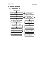
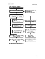
Page 63: ...Trouble Shooting 58 6 Trouble Shooting 6 1 Tungsten lamp off...
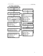
Page 69: ...Trouble Shooting 64 6 8 Slit check failed Only for UV 2802S UV 2802PCS...
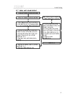
Page 72: ...Trouble Shooting 67 6 13 Get dark current for a long time...
Page 74: ...Trouble Shooting 69 6 15 Backlight OK but display nothing on LCD Display...
Page 77: ...Trouble Shooting 72 6 18 No DC 12V on PCB SST8 412 113...