Electronic System
- 40 -
Pin 3, 4, 5:
DC +12V
Pin 8, 9, 10:
GND
J2---To (Main) Amplifier PCB
Pin 1:
DC +9V
Pin
2:
GND
Pin
3:
DC
-9V
J3---To Transferring PCB(In Upper Case)
Pin (1, 3):
AC 1200V
J4---To Main CPU PCB
Pin 1, 2:
DC +12V
Pin 3, 4:
GND
Pin 5, 6:
DC +5V
J5---To Slave Amplifier PCB
Pin 1:
DC +9V
Pin
2:
GND
Pin
3:
DC
-9V
5.2 Control and Drive System
The working principle as follow (shown in figure 5.10, 5.11 and 5.12):
1. User setup the “Test Parameters” by operating the Keypad. The main
CPU (on “Main CPU PCB”) command the motor to goto the setup
wavelength, select the correct light source and filter;
2. Halogen or deuterium lamp to supply the light, the Monochromator to
isolate the wavelength of interest and eliminate the unwanted second
order radiation, the sample compartment to accommodate the sample
solution;
3. The detector to receive the transmitted light and convert it to an
electrical signal, the slave CPU (on “Slave CPU PCB”) control to
amplifier the electrical signal and convert it to be digital signal, send it to
main CPU;
4. The main CPU gets the digital signal, process and outputs the results
(display, print or send to PC, and so on).
Summary of Contents for SQ Series
Page 5: ......
Page 8: ...Introduction 3 Figure 1 5 Model UV 4802...
Page 12: ...Layout 7 Figure 3 2 Layout of UV 2800 Inside Bottom View...
Page 13: ...Layout 8 39 40 41 42 43 Figure 3 3 Layout of UV 2800 Top View...
Page 14: ...Layout 9 230V 44 45 46 47 48 49 50 51 Figure 3 4 Layout of UV 2800 Back View...
Page 18: ...Layout 13 Figure 3 7 Layout of UV 2802 S UV 2802PC S Inside Bottom View...
Page 19: ...Layout 14 43 44 45 46 47 Figure 3 8 Layout of UV 2802 S Top View...
Page 20: ...Layout 15 230V Figure 3 9 Layout of UV 2802 S UV 2802PC S Back View...
Page 23: ...Layout 18 Figure 3 11 Layout of UV 3802 Inside Bottom View...
Page 24: ...Layout 19 44 45 46 47 48 Figure 3 12 Layout of UV 3802 Top View...
Page 25: ...Layout 20 230V Figure 3 13 Layout of UV 3802 Back View...
Page 28: ...Layout 23 Figure 3 14 Layout of UV 4802 Inside Top View...
Page 29: ...Layout 24 Figure 3 15 Layout of UV 4802 Inside Bottom View...
Page 30: ...Layout 25 43 44 45 46 47 Figure 3 16 Layout of UV 4802 Top View...
Page 31: ...Layout 26 230V Figure 3 17 Layout of UV 4802 Back View...
Page 35: ...Optical 30 Figure 4 3 Optical System schematic diagram of UV 4802...
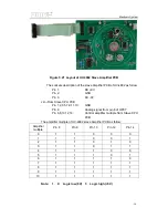
Page 49: ...Electronic System 44 Figure 5 13 Layout of Main CPU PCB...
Page 63: ...Trouble Shooting 58 6 Trouble Shooting 6 1 Tungsten lamp off...
Page 69: ...Trouble Shooting 64 6 8 Slit check failed Only for UV 2802S UV 2802PCS...
Page 72: ...Trouble Shooting 67 6 13 Get dark current for a long time...
Page 74: ...Trouble Shooting 69 6 15 Backlight OK but display nothing on LCD Display...
Page 77: ...Trouble Shooting 72 6 18 No DC 12V on PCB SST8 412 113...


