


LEON-G100 / LEON-G200 - System Integration Manual
GSM.G1-HW-09002-G3
Preliminary
System description
Page 71 of 125
If the
ADC1
pin is not used, it can be left floating on the application board.
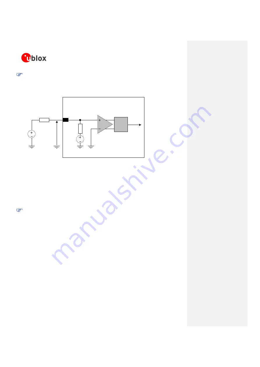
The electrical behavior of the measurement circuit in voltage mode can be modeled by a circuit equivalent to
that shown in Figure 42. This includes a resistor (R
eq
), voltage source (U
eq
), analog preamplifier (with typical gain
G=0.5), and a digital amplifier (with typical gain g
ADC
=2048 LSB/V).
LEON-G100
ADC1
Ueq
Req
Usig
Rsig
Uadc
G
5
g
ADC
Figure 42: Equivalent network for ADC single-ended measurement
The ADC software driver takes care of the parameters shown in Figure 42 (R
eq
, U
eq
, G, g
ADC
): the voltage
measured by
ADC1
is U
adc
and its value expressed in mV is given by the AT+UADC=0 response (for more details
on the AT command refer to
u-blox AT Commands Manual
[2]).
The detailed electrical specifications of the Analog to Digital Converter input (Input voltage span, Input resistance
in measurement mode R
eq
, Internal voltage U
eq
): are reported in the
LEON-G100 / LEON-G200
As described in the ADC equivalent network shown in Figure 42, one part of the whole ADC circuit is outside
the module: the (U
sig
) and the (R
sig
) are characteristics of the application board because they represent the
Thévenin's equivalent of the electrical network developed on the application board.
If an external voltage divider is implemented to increase the voltage range, check the input resistance in
measurement mode (Req) of
ADC1
input and all the electrical characteristics.
If the Thévenin's equivalent of the voltage source (U
sig
) has a significant internal resistance (R
sig
) compared to the
input resistance in measurement mode (R
eq
) of the ADC, this should be taken into account and corrected to
properly associate the AT+UADC=0 response to the voltage source value, implementing the ADC calibration
procedure suggested in the section 1.11.1 below.
If the customer implements the calibration procedure on the developed application board, the influence of the
internal series resistance (R
sig
) of the voltage source (U
sig
) is taken into account in the measurement: the
AT+UADC=0 response can be correctly associated to the value of the voltage source applied on the application
board.
1.11.1
ADC Calibration
To improve the absolute accuracy of the 12-bit analog-to-digital converter (ADC), it is suggested to follow the
calibration procedure here described.
The calibration aim is to evaluate the relationship between the value, expressed in mV, of the voltage source
(V_S, which Thévenin's equivalent is represented by U
sig
and R
sig
shown in Figure 42) that has to be measured and
the AT+UADC=0 response (ADC_VALUE, that is the U
adc
value expressed in mV) when V_S is applied, calculating
the calibration GAIN and OFFSET parameters value.


