
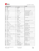
AMY-5M
-
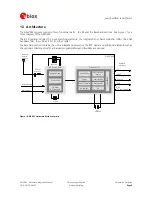
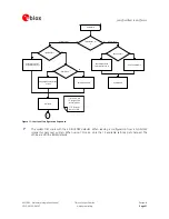
Hardware
Integration
Manual
Objective
Specification
Design-In
GPS.G5-MS5-08207
u-blox
proprietary
Page 12
your position is our focus
An
additional
monitor
switches
the
supply
of
the
back-up
region
VDD_B
from
VDD_IO
to
V_BCKP,
once
VDD_IO
falls
below
its
operational
specification.
Thus,
a
separate
supply
source
can
be
used
to
maintain
RTC
and
backup
RAM
information
even
if
VDD_IO
fails.
If
this
feature
is
not
needed,
V_BCKP
must
be
connected
to
either
VDCDC
or
GND.
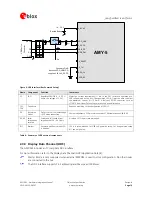
2.1.1.7
USB Interface Power Supply
VDD_USB
supplies
the
I/Os
of
the
USB
interface.
If
the
USB
interface
is
not
used,
the
VDD_USB
pin
must
be
connected
to
GND.
If
the
application
uses
USB,
the
correct
USB
power
mode
needs
to
be
configured
(bus-powered
or
self
powered).
See
the
u-blox 5 Protocol Specification
[3].
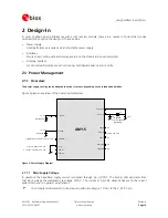
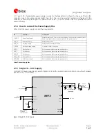
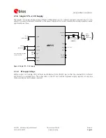
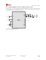
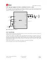
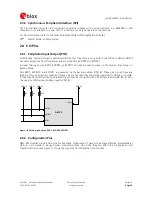
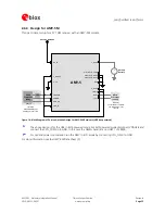
2.1.2 Power Management Configuration
Depending
on
the
application,
the
power
supply
schematic
will
differ.
Some
examples
are
shown
in
the
following
sections:
•
Supply
voltage
nominal
3.3
V
(2.5
–
3.6
V)
see
section
2.1.5
•
Supply
voltage
nominal
1.8
V
(1.75
–
2.0
V)
see
section
2.1.6
•
Direct
supply
of
core
voltages
(VDD_RF,
VDD_3V
1.8
V,
V_DCDC
1.4
V)
see
section
2.1.7
•
Dual
power
supply
using
3.0V
and
1.4V
(VDD_3V
3.0
V,
V_DCDC
1.4
V)
see
section
2.1.8
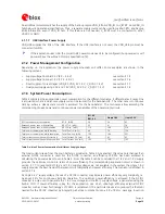
2.1.3 System Power Consumption
Table
2
compares
the
approximate
power
consumption
for
the
different
scenarios.
It
differentiates
2
cases.
One
is
acquisition
where
a
worst-case
supply
current
is
assumed
for
the
base-band-IC.
The
other
case
is
continuous
tracking
where
a
steady
state
current
is
assumed
for
the
base-band-IC.
The
two
cases
allow
assessing
the
dimensioning
of
peak
power
and
continuous
power
capabilities
of
the
power
supply
circuit.
RF 1.8 V
BB 1.4 V
Single 1.8V
Single 3.3V
RF
Front
end
power
consumption
RF-IC
[mW]
34
34
63
Baseband
power
cons.
while
tracking
BB-IC
Trk.
[mW]
32
41
76
Baseband
power
cons.
while
acquisition
BB-IC
Acq.
[mW]
116
149
274
Total
power
consumption
while
tracking
Total
Pwr.Trk.
[mW]
66
76
139
Total
power
consumption
while
acquisition
Total
Pwr.
Acq
[mW]
150
184
337
Total
current
consumption
while
tracking
Total
Current
Trk.
[mA]
42
42
42
Total
current
consumption
while
acquisition
Total
Current
Acq.
[mA]
102
102
102
Table 2: u-blox 5 Power Consumption for different Supply Voltages
The
total
current
drawn
from
the
main
battery
is
provided
in
Table
2.
As
expected,
this
value
only
changes
if
an
external
DC/DC
converter
is
used.
For
the
DC/DC
converter,
an
efficiency
of
80%
has
been
assumed
in
calculating
the
power
values
shown
in
Table
2.
From
this
table
it
can
be
concluded
that
1.4
V
and
1.8
V
supply
provides
the
optimum
solution
in
terms
of
power
efficiency.
The
corresponding
application
circuit
is
shown
in
section
2.1.7.
In
case
distinct
1.4
V
and
1.8
V
supply
voltages
are
not
available
in
the
system,
the
single
1.8
V
supply
provides
the
best
trade-off
between
circuit
complexity
and
power
efficiency.
This
scenario
is
described
in
section
2.1.6.
At
single
3.3
V
supply
voltage
the
use
of
a
DC/DC
converter
may
increase
power
efficiency
only
marginally,
i.e.
by
about
22%
for
continuous
tracking
operation.
The
optimum
power-efficiency
is
achieved
if
the
DC/DC
converter
is
only
used
to
generate
the
1.4
V
core
voltage
and
the
RF-IC
supply
voltage
is
generated
using
the
built-in
LDO.
If
power-efficiency
is
key
for
the
application,
use
of
an
ultra-high
efficiency
external
DC/DC
converter
such
as
Linear
Technology’s
LTC3410
is
recommend.
This
particular
device
also
reduces
the
footprint
needed
for
the
DC/DC
converter
by
integrating
all
active
components
into
a
2.8
×
18
mm
2
package.
In
section


