

AMY-5M
-
Hardware
Integration
Manual
Objective
Specification
Design-In
GPS.G5-MS5-08207
u-blox
proprietary
Page 11
your position is our focus
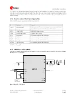
2.1.1.2
Base-Band I/O Supply Voltage
In
general,
the
digital
I/Os
of
the
base-band
part
are
supplied
with
VDD_IO
from
the
host
system.
The
wide
range
of
VDD_IO
allows
seamless
interfacing
to
standard
logic
voltage
levels.
VDD_IO
must
be
supplied
in
any
case
with
a
voltage
in
the
specified
range,
as
some
CFG_xx
pins
are
always
read
during
system
boot
in
order
to
define
the
initial
configuration
of
the
receiver.
The
power
management
unit
does
not
supervise
VDD_IO.
External
circuitry
must
guarantee
that
VDD_IO
is
within
operating
specification
before
the
system
boots
and
that
it
remains
within
specification
until
the
system
shuts
down.
See
also
section
2.1.1.6.
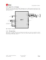
2.1.1.3
Base-Band Core Voltages
The
core
voltages
VDD_B
and
VDD_C
core
are
generated
separately,
in
order
to
enable
main
supply
VDD_C
switch
off
while
the
back-up
domain
VDD_B
remains
alive.
The
core
voltages
are
generated
by
means
of
internal
LDOs.
The
input
voltage
range
of
the
LDOs
is
wide
and
allows
the
use
of
several
types
of
batteries.
2.1.1.4
Backup Power Supply
A
backup
battery
can
be
connected
to
supply
the
RTC
and
the
backup
RAM
in
case
of
power
failure
at
the
main
battery
(VDD_IO).
An
internal
switch
will
supply
the
internal
VDD_B
power
domain
in
case
VDD_IO
drops
below
the
specified
minimum
value.
VDD_IO
will
supply
the
VDD_B
power
domain
if
a
sufficiently
high
input
voltage
is
detected.
See
also
section
2.1.1.6.
It
is
recommended
to
limit
V_BCKP
and
VDD_IO
to
3.6
V.
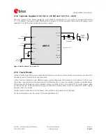
2.1.1.5
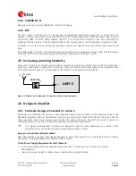
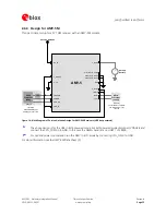
RF Supply Voltages
The
main
supply
of
the
RF
unit
is
1.8
V
supplied
to
the
VDD_RF
pin.
Optionally,
this
voltage
can
be
generated
with
the
internal
LDO
from
the
VDD_3V
input.
Depending
on
the
application,
the
VDD_3V
pin
can
be
supplied
independently,
or
it
can
be
connected
to
the
V_DCDC.
VDD_RF
must
be
a
clean
supply
to
obtain
optimal
performance.
Since
the
V_DCDC
current
is
very
dynamic,
a
filter
is
recommended
to
ensure
little
or
no
ripple
on
VDD_RF.
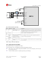
2.1.1.6
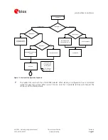
Built-In Supply Voltage Monitors
Built-in
supply
voltage
monitors
ensure
that
the
system
always
operates
in
safe
regions.
The
following
conditions
need
to
be
met
in
order
the
system
to
run
properly:
1.
The
core
voltages
VDD_C
and
VDD_B
need
to
be
within
specification.
These
voltages
are
supervised
by
internal
supply
monitors
(signals
POR_C
and
POR_B
in
Figure
2)
2.
The
RF
supply
voltage
VDD_RF
needs
to
be
within
specification.
3.
IF
external
memory
(FLASH/EEPROM)
is
used,
its
supply
voltage,
i.e.
VDD_IO,
needs
to
be
within
the
specification
of
this
part
With
respect
to
points
2
and
3
listed
above,
the
voltage
that
defines
the
lowest
operational
boundary
condition
of
the
system
shall
be
supervised
at
the
V_RESET
pin.
This
is
usually
either
the
TCXO
supply
voltage
(VDD_3V)
or
the
RF
IC
supply
voltage
(VDD_RF).
In
designs
using
FLASH/EEPROM
memory
it
may
also
be
VDD_IO.
Normally,
higher
system
supply
voltages
take
longer
to
rise
and
fall
faster
than
lower
supply
voltages.
E.g.
if
in
a
given
application,
the
RF
section
requires
1.8
V
but
external
FLASH
memory
requires
2.7
V,
it
is
advisable
to
monitor
VDD_IO
rather
than
VDD_RF.
The
threshold
at
V_RESET
for
releasing
the
MR_N
master
reset
signal
can
be
configured
using
the
V_TH
pin.
It
can
be
set
to
either
2.5
V
or
1.8
V.
If
V_TH
is
open,
the
threshold
is
set
to
1.8
V,
if
this
pin
is
connected
to
GND
the
threshold
is
at
2.5
V.
Internally,
VDD_B
and
VDD_C
are
supervised
by
power-on
reset
circuits.
Reset
signals
on
backup
and
core
domains
POR_B
and
POR_C
are
only
released
once
the
respective
supply
voltages
fall
within
the
operational
conditions.


