


tains plus " + " potential, the waveform moves upward
and if it contains minus " —" potential, the waveform
moves downward.
The reference point of " 0 " potential is checked at
GND position.
A P P L I C A T I O N S
D U A L - T R A C E A P P L I C A T I O N S
Introduction:
The most obvious and yet the most useful feature of the
dual-trace oscilloscope is that it has the capability for
simultaneously viewing two waveforms that are frequency-
or phase-related, or that a common synchronizing voltage,
such as in digital circuitry. Simultaneous viewing of input
and its output is an invaluable aid to the circuit designer or
the repairman. Several possible applications of the
dual-trace oscilloscope will be reviewed in detail to
familiarize the user further in the basic operation of this os-
cilloscope.
Frequency Divider Waveforms Viewing:
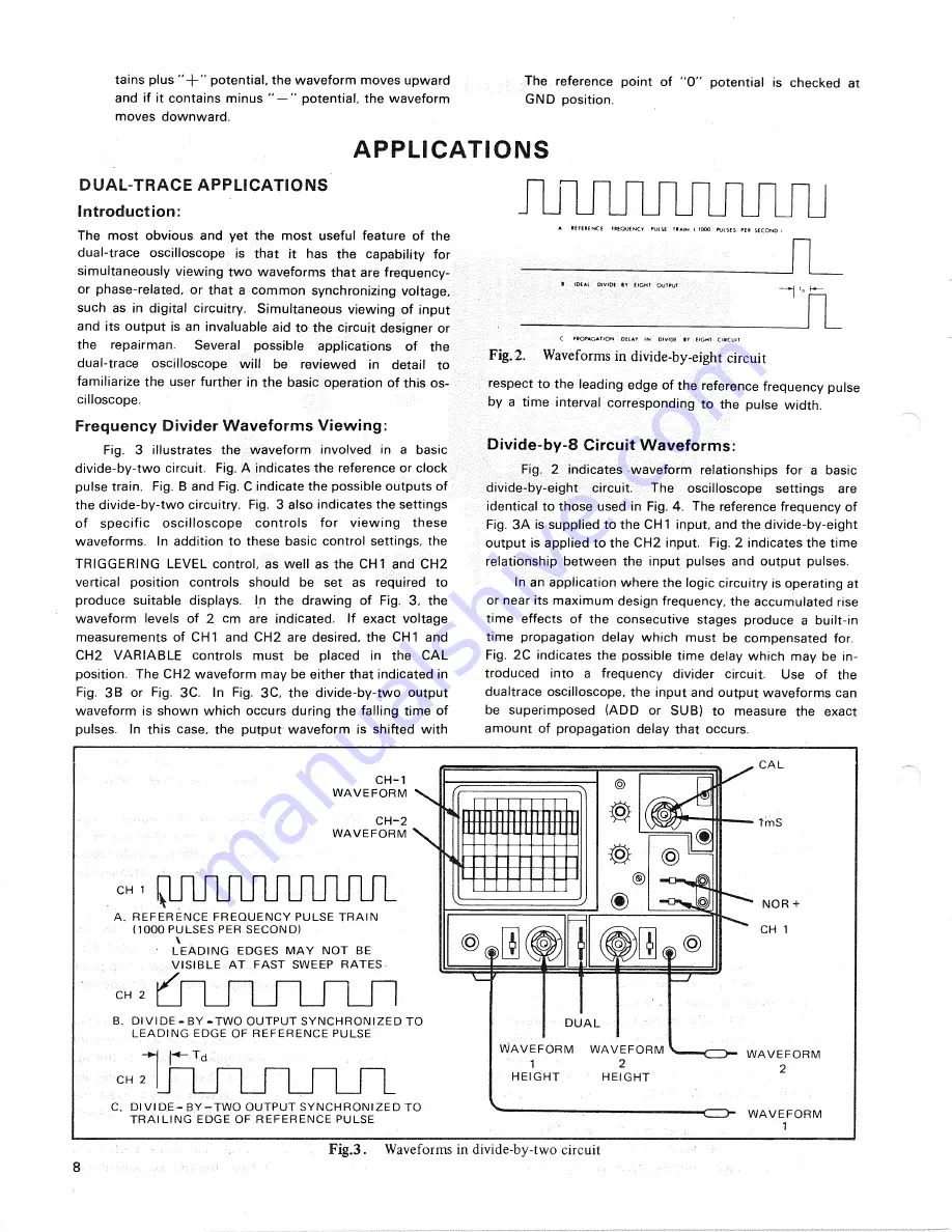
Fig. 3 illustrates the waveform involved in a basic
divide-by-two circuit. Fig. A indicates the reference or clock
pulse train. Fig. B and Fig. C indicate the possible outputs of
the divide-by-two circuitry. Fig. 3 also indicates the settings
of specific oscilloscope controls for viewing these
waveforms. In addition to these basic control settings, the
TRIGGERING LEVEL control, as well as the CH1 and CH2
vertical position controls should be set as required to
produce suitable displays. In the drawing of Fig. 3, the
waveform levels of 2 cm are indicated. If exact voltage
measurements of CH1 and CH2 are desired, the CH1 and
CH2 V A R I A B L E controls must be placed in the C A L
position. The CH2 waveform may be either that indicated in
Fig. 3 B or Fig. 3C. In Fig. 3C, the divide-by-two output
waveform is shown which occurs during the falling time of
pulses. In this case, the putput waveform is shifted with
respect to the leading edge of the reference frequency pulse
by a time interval corresponding to the pulse width.
Divide-by-8 Circuit
Waveforms:
Fig. 2 indicates waveform relationships for a basic
divide-by-eight circuit. The oscilloscope settings are
identical to those used in Fig.
4.
The reference frequency of
Fig. 3A is supplied to the CH1 input, and the divide-by-eight
output is applied to the CH2 input. Fig. 2 indicates the time
relationship between the input pulses and output pulses.
In an application where the logic circuitry is operating at
or near its maximum design frequency, the accumulated rise
time effects of the consecutive stages produce a built-in
time propagation delay which must be compensated for.
Fig. 2C indicates the possible time delay which may be in-
troduced into a frequency divider circuit. Use of the
dualtrace oscilloscope, the input and output waveforms can
be superimposed (ADD or SUB) to measure the exact
amount of propagation delay that occurs.
C H - 1
W A V E F O R M
C H - 2
W A V E F O R M
CH 1
A. R E F E R E N C E F R E Q U E N C Y P U L S E T R A I N
( 1 0 0 0 P U L S E S PER SECOND)
CH
2
B. D I V I D E - B Y - T W O OUTPUT S Y N C H R O N I Z E D T O
L E A D I N G E D G E OF R E F E R E N C E P U L S E
CH
2
C. D I V I D E - B Y - T W O OUTPUT S Y N C H R O N I Z E D T O
T R A I L I N G E D G E OF R E F E R E N C E P U L S E
W A V E F O R M
2
W A V E F O R M
1
Fig
.3
. Waveforms in divide-by-two circuit
Fig.
2.
Waveforms in divide-by-eight circuit
L E A D I N G E D G E S M A Y NOT B E
V I S I B L E A T F A S T SWEEP R A T E S
W A V E F O R M
1
H E I G H T
W A V E F O R M
2
H E I G H T
8


