BIOS SETUP
28
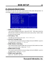
3.5 Advanced Chipset Features
This option will change the values of the chipset registers and the system settings will alter. Do
not change any values if you are unfamiliar with the chipset.
•
DRAM Timing Selectable
This controls the SDRAM performance: default is “By SPD”. BIOS will auto detect the
SPD information of the Memory Module and choose the proper setting. “By User” allows
the timing to be set manually.
•
CAS Latency Time
This allows the CAS Latency to be set to: “1.5”, “2”, “2.5”, or “3”.
•
Active to Precharge Delay
This controls the idle clocks after issuing a precharge command to SDRAM. Leave it on
the default setting. Options are: “7”, “6”, or “5”.
•
DRAM RAS# to CAS# Delay
This controls the latency between DRAM active command and the read/write command.
Leave it on the default setting. Options are: “3” or “2”.
•
DRAM RAS# Precharge
This controls the idle clocks after issuing a precharge command to SDRAM. Leave it on
the default setting. Options are: “3” or “2”.
•
DRAM Data Integrity Mode
Options are: “Non-ECC” and “ECC”.
Transcend Information, Inc.


