


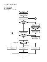


Disc kind misjudgement
(Initial setting is NG.)
Replace pickup head.
Lens cleaning.
Check IC502.
Are FE and RFSB
signals for each disc normal?
Check peripheral
circuit of IC604.
2-2
Y
N
Check laser current.
Check laser current.
50 mA lop 90 mA
Check pins 14, 15
and 16 of IC502
serial bus.
Check peripheral
circuits of IC502,
Q501.
lop = Voltage between
(E534 and E536)/10
W
Replace pickup
mechanism.
Check wiring for
pickup head.
Check peripheral circuits
of IC502, Q501.
lop 90 mA
lop 50 mA
3
Y
Fig. 1-3-4
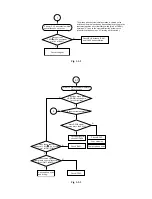
Fig. 1-3-5
DVD single (single-layer) disc
detection waveform
FE signal
Pin150 (TP405) of IC401
RFSB signal
Pin152 (TP503) of IC401
1.65V
V : 500 mV/div
H : 2 ms/div
DVD dual (dual-layer) disc
detection waveform
V : 500 mV/div
H : 2 ms/div
CD disc
detection waveform
V : 500 mV/div
H : 2 ms/div
Fig. 1-3-6
Fig. 1-3-7
Fig. 1-3-8
Summary of Contents for SD-2050
Page 1: ...DVD VIDEO PLAYER SERVICE MANUAL May 2000 s FILE NO 810 200005 SD 2050 DIGITAL VIDEO ...
Page 5: ...SECTION 1 GENERAL DESCRIPTIONS SECTION 1 GENERAL DESCRIPTIONS 1 OPERATING INSTRUCTIONS ...
Page 51: ...47 Others Memo ...
Page 80: ...4 2 Power Supply Block Diagram Fig 3 4 2 ...
Page 82: ...Fig 3 4 5 4 3 3 Front Display Power Switch Block Diagram ...
Page 84: ...Fig 3 4 7 4 4 2 Logical System Block Diagram ...
Page 85: ...4 5 Output Block Diagram Fig 3 4 8 ...
Page 88: ...10 1 3 4 A B C D E G 2 5 6 7 8 9 F Fig 3 5 3 5 2 Front Display Power Switch Circuit Diagram ...
Page 95: ...Fig 3 5 5 5 3 2 Main Circuit Diagram ...
Page 96: ...5 3 2 Main Circuit Diagram ...
Page 97: ......
Page 98: ......
Page 99: ......
Page 100: ......
Page 101: ......
Page 102: ......
Page 103: ...Fig 3 5 5 ...
Page 105: ...Fig 3 5 6 10 1 3 4 A B C D E G 2 5 6 7 8 9 F 11 H 5 4 Output Circuit Diagram ...
Page 115: ...10 1 3 4 A B C D E G 2 5 6 7 8 9 F Fig 3 6 6 EU01 Main PC Board Top pattern character symbol ...
Page 125: ......


