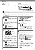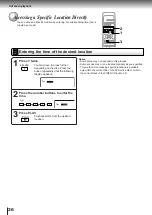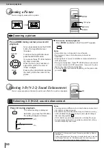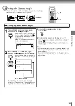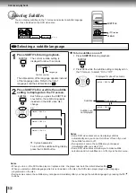
22
Basic playback
Playing a Disc (continued)
You can play discs at various speeds, and resume playback from the location
where you stopped playback.
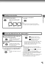
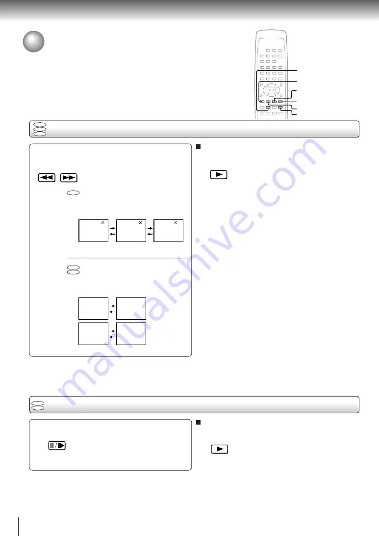
Playing fast in reverse or forward direction
To resume normal playback
Press PLAY.
Notes
• The DVD video player does not play sound and subtitles
during reverse and forward scan of DVD video discs.
However, the DVD video player plays sound during fast
forward or fast reverse play of audio CDs.
• The playback speed may differ depending on the disc.
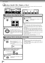
Playing frame by frame
Press PAUSE/STEP during still playback.
Each time you press the PAUSE/
STEP button, the picture advances
one frame.
To resume normal playback
Press PLAY.
Note
The sound is muted during frame by frame playback.
DVD
VCD
CD
DVD
VCD
PAUSE/STEP
PLAY
PLAY
FWD
REV
PAUSE/STEP
PLAY
SLOW
STOP
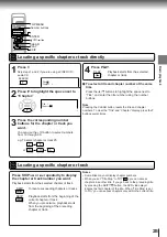
Press REV or FWD during playback.
REV: Fast reverse playback
FWD: Fast forward playback
Each time you press the REV or
FWD button, the playback speed
changes.
Each time you press the REV or
FWD button, the two speeds
alternate.
TV screen
x2 the normal
speed
x8 the normal
speed
x30 the normal
speed
TV screen
Fast reverse
playback
Fast forward
playback
VCD
CD
DVD
FR1
FR2
FF1
FF2
2
8
30
REV
FWD
Summary of Contents for SD-2050
Page 1: ...DVD VIDEO PLAYER SERVICE MANUAL May 2000 s FILE NO 810 200005 SD 2050 DIGITAL VIDEO ...
Page 5: ...SECTION 1 GENERAL DESCRIPTIONS SECTION 1 GENERAL DESCRIPTIONS 1 OPERATING INSTRUCTIONS ...
Page 51: ...47 Others Memo ...
Page 80: ...4 2 Power Supply Block Diagram Fig 3 4 2 ...
Page 82: ...Fig 3 4 5 4 3 3 Front Display Power Switch Block Diagram ...
Page 84: ...Fig 3 4 7 4 4 2 Logical System Block Diagram ...
Page 85: ...4 5 Output Block Diagram Fig 3 4 8 ...
Page 88: ...10 1 3 4 A B C D E G 2 5 6 7 8 9 F Fig 3 5 3 5 2 Front Display Power Switch Circuit Diagram ...
Page 95: ...Fig 3 5 5 5 3 2 Main Circuit Diagram ...
Page 96: ...5 3 2 Main Circuit Diagram ...
Page 97: ......
Page 98: ......
Page 99: ......
Page 100: ......
Page 101: ......
Page 102: ......
Page 103: ...Fig 3 5 5 ...
Page 105: ...Fig 3 5 6 10 1 3 4 A B C D E G 2 5 6 7 8 9 F 11 H 5 4 Output Circuit Diagram ...
Page 115: ...10 1 3 4 A B C D E G 2 5 6 7 8 9 F Fig 3 6 6 EU01 Main PC Board Top pattern character symbol ...
Page 125: ......


