background image

2.5      2.5-inch HDD 

2  Troubleshooting 

Satellite A100/A105 / TECRA A7   Maintenance Manual


2-13 

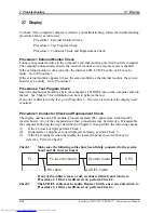
create a DOS partition on drive C.  Then restart the computer..  If the 
problem persists, go to Procedure 3. 


Summary of Contents for Satellite A100 Series

Page 1: ...Satellite A100 A105 TECRA A7 Maintenance Manual Toshiba Personal Computer Satellite A100 A105 TECRA A7 PSAA8 PSAA9 PTA70 PTA71 PSAAx Maintenance Manual TOSHIBA CORPORATION ...

Page 2: ...ii S No ...

Page 3: ...ECRA A7 at the time of this manual s production However succeeding computers and manuals are subject to change without notice Therefore Toshiba assumes no liability for damages incurred directly or indirectly from errors omissions or discrepancies between any succeeding product and this manual Trademarks Intel and Pentium are registered trademarks of Intel Corporation IBM IBM PC XT PC AT PS 2 and ...

Page 4: ...ning indicates the existence of a hazard that could result in bodily injury if the safety instruction is not observed CAUTION Caution indicates the existence of a hazard that could result in property damage if the safety instruction is not observed NOTE Note contains general information that relates to your safe maintenance service Improper repair of the computer may result in safety hazards Toshi...

Page 5: ...Procedures explains how to diagnose and resolve FRU problems Chapter 3 Test and Diagnostics describes how to perform test and diagnostic operations for maintenance service Chapter 4 Replacement Procedures describes the removal and replacement of the FRUs Appendices The appendices describe the following Handling the LCD module Board layout Keyboard scan character codes Key layout Wiring diagrams BI...

Page 6: ...pears on the keyboard is printed in boldface type Key operation Some operations require you to simultaneously use two or more keys We identify such operations by the key top symbols separated by a plus sign For example Ctrl Pause Break means you must hold down Ctrl and at the same time press Pause Break If three keys are used hold down the first two and at the same time press the third User input ...

Page 7: ...ries 20 1 1 1 Main Battery 20 1 1 2 Battery Charging Control 20 1 1 3 RTC Battery 21 Chapter 2 Troubleshooting 2 1 Outline 2 1 2 2 Basic Flowchart 2 2 2 3 Power Supply 2 6 Procedure 1 Power Icon Check 2 6 Procedure 2 Connection Check 2 8 Procedure 3 Replacement Check 2 8 2 4 System Board 2 9 Procedure 3 Replacement Check 2 10 2 5 2 5 inch HDD 2 11 Procedure 1 Message Check 2 11 Procedure 2 Partiti...

Page 8: ...cedure 3 Connector Check and Replacement Check 2 18 2 9 LAN 2 20 Procedure 1 Test Program Check 2 20 Procedure 2 Connector Check and Replacement Check 2 20 2 10 SD MS MS pro MMC XD Card Optional 2 21 Procedure 1 Test Program Check 2 21 Procedure 2 Connector Check 2 21 2 11 Finger Print Optional 2 22 Procedure 1 Test Program Check 2 22 Procedure 2 Connector Check 2 22 2 12 3D Sensor 2 23 Procedure ...

Page 9: ... Quick Start 3 3 2 1 Quick Test 3 3 2 2 Customization Test 3 3 2 3 Keyboard Layout test 7 3 2 4 Hotkey Test 8 3 2 5 Audio Play Test 8 3 2 6 Audio Record Test 8 3 2 7 DMI Read 8 3 2 8 DMI Write 9 3 2 9 3D Sensor Test 10 3 2 10 FPRD Test 16 3 2 11 FENR Test 16 3 2 12 IrDA ManMaster Test 16 3 2 13 IrDA ManSlave Test 17 3 2 14 System Information 17 3 2 15 View Logs 19 3 2 16 Exit to MS DOS 19 3 2 17 T...

Page 10: ...h Parameters 28 3 3 6 LOG Parameters Setting 28 3 3 7 Specify LOG Viewer 29 3 3 8 Display LOG File 30 3 3 9 LOG Viewer 30 3 3 10 LOG File Sample 32 3 4 Subtests 33 3 5 System Test 36 3 6 Memory Test 40 3 7 Storage 46 3 8 Video 50 3 9 Communication COMM 59 3 10 Peripheral 61 3 11 Error Codes and description 63 3 12 Quick Test Item List i ...

Page 11: ...ack 4 8 Installing the Battery Pack 4 9 Removing the PCI Expresss Card 4 10 Installing the PCI Expresss Card 4 11 Removing the Optional PC Card 4 12 Installing the Optional PC Card 4 13 Removing the Momery Card 4 14 Installing the Momery Card 4 15 Removing the Optional Memory 4 16 Installing the Optional Memory 4 18 Removing the MDC Card 4 19 Installing the MDC Card 4 21 4 2 HDD 4 22 Removing the ...

Page 12: ...the Display Assembly 4 34 Installing the Display Assembly 4 35 4 8 Top Cover 4 36 Removing the Top Cover 4 36 Installing the Top Cover 4 38 4 9 CPU Cooling Module and Fan 4 39 Removing the CPU Cooling and Fan for VGA Card Model 4 39 Installing the CPU Cooling and Fan for VGA Card Model 4 41 Removing the CPU Cooling and Fan 4 42 Installing the CPU Cooling and Fan 4 43 4 10 VGA Card for VGA Card Mod...

Page 13: ...57 Removing the 15 4 inch LCD module 4 57 Installing the 15 4 inch LCD Module 4 59 4 17 Speakers 4 60 Removing the Speakers 4 60 Installing the Speakers 4 60 4 18 Switch Cover and Switch Board 4 61 Removing the Switch Cover and Switch Board For Consumer Model 4 61 Installing the Switch Cover and Switch Board 4 62 Removing the Switch Cover and Switch Board For Commercial Model 4 63 Installing the S...

Page 14: ... A Handling the LCD Module A 1 Appendix B Board Layout B 1 Appendix C Keyboard Scan Character Codes C 1 Appendix D Key Layout D 1 Appendix E Wiring Diagrams E 1 Appendix F BIOS Rewrite Procedures F 1 Appendix G EC KBC Rewrite Procedures G 1 Appendix H GREASE NFORMATION H 1 ...

Page 15: ...Chapter 1 Hardware Overview ...

Page 16: ...1 Hardware Overview ii Satellite A100 A105 TECRA A7 Maintenance Manual ...

Page 17: ...ter 1 Contents 1 1 Features 1 1 2 System Unit Components 9 1 3 2 5 inch HDD 15 1 4 DVD ROM Drive 16 1 5 CD RW DVD ROM Drive 17 1 6 DVD Super Multi R Double Layer 18 1 7 Power Supply 19 1 8 Batteries 20 1 1 1 Main Battery 20 1 1 2 Battery Charging Control 20 1 1 3 RTC Battery 21 ...

Page 18: ...configuration 8 Figure 1 4 System unit block diagram 9 Figure 1 5 2 5 inch HDD 15 Figure 1 6 DVD ROM drive 16 Tables Table 1 1 2 5 inch HDD specifications 15 Table 1 2 DVD ROM drive specifications 16 Table 1 3 CD RW DVD ROM drive specifications 17 Table 1 4 DVD Super Multi drive R Double Layer specifications 18 Table 1 5 Battery specifications 20 Table 1 6 Quick normal charging time 21 ...

Page 19: ...puter has the following features Processor The CPU is the Intel Yonah Processor and Intel Yonah based Celeron M Intel Yonah Processor 667MHz T2300 1 66G T2400 1 83G T2500 2G T2600 2 16G T2700 2 33G T1300 1 66G T1400 1 83G Hz Intel Yonah based Celeron M Processor 533MHz 410 420 430 Host bridge system controller System controller Intel 945GM 945PM 940GML Memory The computer has two SO DIMMs slot com...

Page 20: ...h brightness 15 4 WXGA HHCSV 490 NITs High brightness color display resolution 1280 800 262 144 colors with dithering Keyboard The keyboard has 29 kinds countries key Batteries The computer has a removable 6 9 12 Cell Lithium Ion battery pack and an internal RTC battery rechargeable Universal Serial Bus USB ports The computer has four USB 2 0 ports It is supported to daisy chain a maximum of 127 U...

Page 21: ... button and One kind of Dual mode Pad for BTO Sound system The ALC861 integrated audio controller supports multimedia The sound system contains the following Stereo speakers Headphone jack Internal microphone External microphone jack LAN The internal LAN board supports 10 100 Mbit and Giga bit for BTO enabling connection to a LAN at up to 1GMbps It also supports Wake up On LAN From S3 S4 S5 and PX...

Page 22: ... no longer necessary to input the password from the keyboard Just by swiping the finger against the fingerprint sensor TPM 1 2 The Trusted Platform Module TPM is an integrated circuit and software platform that provides computer manufacturers with the core components of a subsystem used to assure authenticity integrity and confidentiality in e commerce transactions and Internet communications CD K...

Page 23: ...rdware Overview Satellite A100 A105 TECRA A7 Maintenance Manual 5 The FIR Port is optional integrated device It provided an IrDA 1 1 compatible FIR port enabling wireless communication at a high speed of 1 15 or 4 Mbps ...

Page 24: ...re Overview 1 1 Features 6 Satellite A100 A105 TECRA A7 Maintenance Manual Figures 1 1 1 2 1 3 and 1 4 show the computer and its system unit configuration respectively Figure 1 1 id Parts description placement ...

Page 25: ...OUT SMS C KBC 1100 FSB 533 667MHz ODD C IR U S B 6 EXPRESSCARD 1 8V DDR2Interface 533 667M Hz Blue to oth HDD R J11 PORT REPLIC ATOR C O N N C U S B 2 C O N N B ICH7 M Wire less LAN 1394 Primary_IDE SIO 1036 3 3V PC I_Interface 33MHz IMVP 6 C O N N A U S B 7 U S B 5 U S B 1 HP J AC K J AC K MIC SPEAKER ANT PARALLEL POR T BIO S DDR2 _SODIMM0 DMIx4 6 52 B GA SMSC 1 8V D DR2Interface 533 667MH z VR A...

Page 26: ... TECRA A7 Maintenance Manual 8 DC IN Kensi ngton Battery Speaker RGB USB 2 Rj45 Rj11 S Video 1394 USB 2 Microphone Headphone Volume Speaker ODD HDD PC Card 1 Express Card 1 Kill SW 5 in 1 Card Reader Parallel FIR CIR Figure 1 3 System Board configuration ...

Page 27: ...CH7 M South Bridge Ac97 IDE Cont USB Cont 02 PCI PC Bridge Int HDD SATA 40 120GB 9 5 m m DVD ROM DVD CD RW COMBO DVD Super Multi R Double layer SATA L A N C o n t 1 0 1 0 0 8 2 5 6 2 G Z 1 G 8 2 5 7 3 E Mini PCI Slot 802 11g a g Wireless Lan A n t e n n a EEPROM R j 4 5 CARD BUS C o n t r o l l e r T I P C I 7 4 1 2 P C I 4 5 1 2 _ 5 i n 1 C a r d R e a d e r PCMCIA 1394 CNNx1 TPA6011 Speaker M I ...

Page 28: ...vel 2 cache 2 MB Advanced Power Management features including Enhanced Intel SpeedStep technology Yonah Based Celeron M 533MHz Core speed TBD System bus 533 MHz On die level 2 cache 1 MB Memory Two expansion memory slots were provided They can hold 256 512 1024MB expansion memory modules available as options to grow up to 4 0 GB PC2 4200 533 667MHz DDRII SDRAM supported 256 512 1024MB modules supp...

Page 29: ...sed for VGA BIOS 42Kb used for PXE 14Kb used for string 47Kb used for ROMEXEC 133Kb used for BIOS code 6Kb used for mini loader System controllers North Bridge Intel 945 GM PM 940GML CPU interface and control System Memory Support PCI Express Graphics PEG Interface Integrated Display Interface Support Internal Graphics Features Direct Media Interface DMI Power Management Serial ATA Interface ICH7 ...

Page 30: ... Pro MMC XD Card controller IEEE 1394 Controller Audio Controller The ALC861 integrated audio controller supports multimedia The sound system feature contains the following 4 Stereo DACs support 16 20 24 bit PCM format for 7 1 channel audio solution 1 stereo ADCs support 16 bit PCM forma t Front Surround Cen Lfe Side Surround DACs support independent 48KHz 96KHz sample rate ADC support 48K 96K sam...

Page 31: ...rt Battery capacity check Flash memory reprogramming function EC access interface I2C communication control Battery EE PROM 24C02 equivalent 128 words x 16 bits I2C interface integrated in the battery pack Storing records of battery use Clock Generator ICS9LP306 Generating the clock signal required for the system Modem Controller Built in MDC card with askey Functions of the modem controller Digit...

Page 32: ...tic detection of unplugged mode Remote boot PXE 2 1 Smart power down when link is not detected 82573E PCIe Power Management Peak bandwidth 2 gigabytes second per direction Digital Adaptive Equalization control Optimized transmit and receive queues On board microcontroller SNMP and RMON statistic counters SDG 3 0 WfM 3 0 and PC2001 compliance Wake on LAN support Wireless LAN controller Support foll...

Page 33: ...ed are 40 60 80 100 120 GB The HDD interface conforming to Serial ATA for 40 60 80 100 120 GB The HDD is shown in Figure 1 5 and some of its specifications are listed in Table 1 1 Figure 1 5 2 5 inch HDD Table 1 1 2 5 inch HDD specifications Item Specifications Capacity GB 40GB 60GB 80GB 100GB 120GB Rotational speed RPM 5400 rpm 5400 rpm 7200 rpm 5400 rpm 7200 rpm 5400 rpm 7200 rpm 5400 rpm User d...

Page 34: ...M and 3 600 Kbytes per second from CD ROM The DVD ROM drive is shown in Figure 1 6 and its specifications are listed in Table 1 2 Figure 1 6 DVD ROM drive Table 1 2 DVD ROM drive specifications Item DVD ROM Data transfer rate Mbytes s 33 3 U DMA transfer mode 2 16 7 PIO mode 4 Multiword DMA mode 2 Access time ms Average random access 100ms Data buffer size Kbytes 512KB Formats supported DVD R W Re...

Page 35: ...eed and CD RW at 4x speed The specifications of the CD RW DVD ROM drive are listed in Table 1 3 Table 1 3 CD RW DVD ROM drive specifications Item DVD ROM mode CD RW mode 33 3 U DMA transfer mode 2 Data transfer rate Mbytes s 16 7 PIO mode 4 Multiword DMA mode 2 Access time ms Average random access 150 ms 130 ms Data buffer size Mbytes 2MB DVD DVD ROM DVD R DVD RAM CD Formats supported CD DA CD E G...

Page 36: ...VD R at 8x speed and DVD R Double Layer at 4x speed and DVD R Double Layer at 4x speed and DVD RW at 8x speed and DVD RAM at 5x speed The specifications of the DVD Super Multi R Double Layer drive are listed in Table 1 4 Table 1 4 DVD Super Multi drive R Double Layer specifications Item DVD ROM mode CD ROM mode 33 3 U DMA transfer mode 2 Data transfer rate Mbytes s 16 6 PIO mode 4 Multiword DMA mo...

Page 37: ...he supply of DC power supply input AC Adapter output to the power supply unit Controls the supply of power to the system block load logic circuit side Controls forced shutdown if the power supply malfunctions 3 Logic circuit control Instructs the gate array to enable disable tuning the power on Controls power on off operation 4 Status display Turns on the Power LED in Blue or Green or AMBER Batter...

Page 38: ...m Ion 10 8 V 8600 mAh RTC battery Lithium Ion 3 0 V 14 mAh 1 1 1 Main Battery The main battery pack serves as the computer s main power source when the AC adapter is not attached The main battery maintains the state of the computer so that it can resume it 1 1 2 Battery Charging Control Battery charging is controlled by LPC 47N249 When the AC adapter and battery pack are attached to the computer t...

Page 39: ...ge time Any of the following cases stops battery charge 1 The battery becomes fully charged 2 The AC adapter or battery pack is removed 3 The battery or AC adapter voltage is abnormal Detection of full charge A full charge is detected only when the battery is being charged by quick or normal charge A full charge is detected when either of the following conditions is met 1 The current in the batter...

Page 40: ...2 Troubleshooting 2 i Satellite A100 A105 TECRA A7 Maintenance Manual 2 Chapter 2 Troubleshooting ...

Page 41: ...k 2 15 Procedure 5Connector Check and Replacement Check 2 16 2 6 Keyboard 2 17 Procedure 1 Test Program Check 2 17 Procedure 2 Connector Check and Replacement Check 2 17 2 7 Display 2 18 Procedure 1External Monitor Check 2 18 Procedure 2Test Program Check 2 18 Procedure 3Connector Check and Replacement Check 2 18 2 8 ODD Optical Disk Drive 2 20 Procedure 1ODD Cleaning Check 2 20 Procedure 2Test Pr...

Page 42: ... 25 Procedure 2Replacement Check 2 25 2 13 Parallel Port Optional 2 26 Procedure 1Test Program Check 2 26 Procedure 2Connector Check 2 26 2 14 Audio Test 2 27 Procedure 1 Test Program Check 2 27 Procedure 2 Connector Check and Replacement Check 2 27 2 15 IEEE 1394 Test 2 28 Procedure 1Test Program Check 2 28 Procedure 2Connector Check 2 28 2 16 Cooling Module 2 29 Procedure 1Test Program Check 2 2...

Page 43: ...2 Troubleshooting 2 iv Satellite A100 A105 TECRA A7 Maintenance Manual Figures Figure 2 1 Basic flowchart 2 3 Tables Table 2 1 HDD error code and status 2 15 ...

Page 44: ...XD 8 Finger Print 9 Speaker 9 IEEE 1394 10 Cooling module See Chapter 4 for the procedures to replace FRUs and Chapter 3 for the procedures to use test programs The following tools are required to perform the diagnostic procedures 1 Diagnostics maintenance test program disk 2 Phillips screwdrivers 2 mm 2 5 mm 3 Cleaning disk kit for ODD drive cleaning 4 Bootable CD 5 PC Card loopback connector 6 M...

Page 45: ...sword has been registered and if so ask him or her to enter the password If the user has forgotten the system password use a jump wire to make a short circuit on M B C88 then turn the computer power on When booted the computer overrides password protection and automatically erases the current password Make sure the Windows XP Home Edition has been installed on the HDD Any other operating system ca...

Page 46: ...uch with Tomorrow Toshiba displayed Follow the power supply diagnostic procedure in Section 2 3 Follow the power supply diagnostic procedure in Section 2 3 Follow the system board diagnostic procedure in Section 2 4 Follow the display diagnostic procedure in Section 2 7 Password displayed OS started See the previous page to delete the password Follow the HDD diagnostic procedure in Section 2 5 Yes...

Page 47: ...h test with the diagnostic program Any error detected by the diagnostic program Perform the continuous test to check if the error is intermittent Follow the ODD diagnostic procedure in Section 2 8 Identify the test resulting in the error and perform the appropriate diagnostic procedures Any error detected by the diagnostic program Identify the test resulting in the error and perform the appropriat...

Page 48: ...the display troubleshooting procedures in Section 2 7 5 If an error is detected by the ODD test follow the ODD troubleshooting procedures in Section 2 8 6 If an error is detected by the LAN test follow the LAN troubleshooting procedures in section 2 9 7 If an error is detected by the SD Card test follow the SD Card troubleshooting procedures in section 2 10 8 If an error is detected by the Finger ...

Page 49: ...k Procedure 2 Connection Check Procedure 3 Replacement Check Procedure 1 Power Icon Check The following two power LEDs indicate the power supply status Battery LED DC IN LED The power supply controller displays the power supply status through the Battery and DC IN LEDs as in the tables below Battery LED Battery LED Power supply status On in Amber Battery being charged On in Green Blue Battery full...

Page 50: ...ng DC in Off Else If the DC IN LED off follow the steps below 1 Remove the battery pack and the AC adapter to shut off power supply to the computer 2 Attach the battery and AC adapter back again If the LED still off follow the steps below Check 1 Make sure the DC IN LED goes on in Green or Blue If it does not go to Procedure 2 Check 2 Make sure the Battery LED goes on in Amber or Blue or Green If ...

Page 51: ...aptor and AC power cord If the DC IN LED does not go on go to Procedure 3 If the battery LED does not go on perform Check 3 Check 3 Make sure the battery pack has been correctly installed in the computer If the battery LED does not go on while the battery pack has been installed correctly go to Procedure 3 Procedure 3 Replacement Check The system board power supply board or CPU may be faulty Disas...

Page 52: ...lowing error message is displayed on the screen press the F1 key as prompted These errors occur when the system configuration preserved in the RTC memory generally called CMOS memory does not match the actual configuration or when the data is lost If you press the F1 key as prompted by the message the TSETUP screen appears to set the system configuration If the error message appears frequently whe...

Page 53: ...2 Troubleshooting 2 4 System Board 2 10 Satellite A100 A105 TECRA A7 Maintenance Manual ...

Page 54: ...e procedures described in Chapter 3 1 System test 2 Memory test 3 Keyboard test 4 Display test 5 Hard Disk test 6 Mouse test 7 SD Card Memory stick test 8 ODD test 9 Sound test 10 LAN test If an error is detected during these tests go to Procedure 3 Procedure 3 Replacement Check The system board memory or CPU may be defective Disassemble the computer following the steps described in Chapter 4 and ...

Page 55: ...ages may appear on the display Follow the steps below to check the HDD Check 1 If either of the following messages appears go to Procedure 2 If the following messages do not appear perform Check 3 Insert system disk in drive Press any key when ready or Non System disk or disk error Replace and press any key Check 2 Check TSETUP to see if the Hard Disk option has been set to Not used If so choose a...

Page 56: ...2 5 2 5 inch HDD 2 Troubleshooting Satellite A100 A105 TECRA A7 Maintenance Manual 2 13 create a DOS partition on drive C Then restart the computer If the problem persists go to Procedure 3 ...

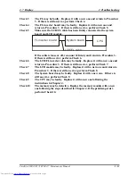
Page 57: ...ears on the display the system files have been transferred to the HDD Restart the computer If the problem persists go to Procedure 3 System transferred NOTE If the computer is running Windows XP Home edition and the hard disk capacity is more than 512 MB the FDISK program will ask if you need support for a partition larger than 2 GB Select Y for large partition support however be sure to read the ...

Page 58: ...ames are listed in Table 2 1 If an error code is not generated and the problem still exists go to Procedure 5 Table 2 1 HDD error code and status Code Status 1 Get Parameter Fail 2 Read Old Data Error 3 Write Pattern Error 4 Read Back Data Error 5 Data Compare Error 6 Restore Data Error 7 Read Verify Error 9 Seek Error 10 Disk Controller Self Test Failed 11 Disk Controller Test unexpected interrup...

Page 59: ...and CPU HDD System board CPU If any connector is loose or off reconnect it firmly and return to Procedure 1 If there is still an error perform Check 2 Check 2 The HDD may be damaged Replace it with a new one following the disassembling instructions in Chapter 4 If the problem persists perform Check 3 Check 3 The System board may be damaged Replace it with a new one following the disassembling inst...

Page 60: ...r following the steps described in Chapter 4 and perform the following checks Check 1 Make sure the keyboard cable has been firmly connected to the system board Keyboard System board CPU If the cable is loose or off reconnect it firmly and return to Procedure 1 If there is still an error perform Check 2 Check 2 The keyboard may be faulty Replace it with a new one following the instructions in Chap...

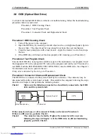
Page 61: ...e Chapter 3 for information on how to perform the test If an error is detected in the test go to Procedure 3 If no error is detected the display itself is normal Procedure 3 Connector Check and Replacement Check The display unit has an LCD module Fluorescent lamp FL panel close switch and FL inverter board Any of the components or their connections may be defective Disassemble the computer followi...

Page 62: ...onnect it firmly and return to Procedure 3 If there is still an error perform Check 6 Check 6 The LCD FL inverter cable may be faulty Replace it with a new one and return to Procedure 3 If there is still an error perform Check 7 Check 7 The LCD module may be faulty Replace it with a new one and return to Procedure 3 If there is still an error perform Check 8 Check 8 The System board may be faulty ...

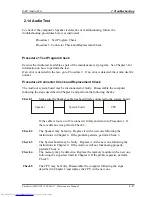
Page 63: ...part of the maintenance test program Insert the diagnostics CD in the computer s CD turn on the computer and run the test Then insert a test ODD Toshiba EMI DVD ROM TEST DISK TSD 1 into the ODD drive See Chapter 3 for information on how to perform the test If any error is detected by the test go to Procedure 3 Procedure 3 Connector Check and Replacement Check The ODD drive is connected to the syst...

Page 64: ...stem board may be faulty Replace it with new one following the instructions in Chapter 4 If the ODD drive is still not functioning properly perform Check 5 Check 5 The memory may be defective Replace the memory module with a new one following the steps described in Chapter 4 If the problem persist perform Check 6 Check 6 The memory may be defective Replace the memory module with a new one followin...

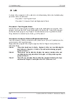
Page 65: ... abnormal is detected by the check go to Procedure 2 Procedure 2 Connector Check and Replacement Check The LAN connector RJ45 is mounted on the system board If the LAN malfunctions the system board or CPU might be faulty Disassemble the computer following the steps described in Chapter 4 and perform the following checks Check 1 The system board may be faulty Replace it with a new one following the...

Page 66: ...rmation on how to perform the test If any error is detected by the test go to Procedure 2 Procedure 2 Connector Check The Memory Card connector is mounted on the system board If the Memory Card malfunctions the system board or CPU might be faulty Disassemble the computer following the steps described in Chapter 4 and perform the following checks Check 1 The system board may be faulty Replace it wi...

Page 67: ...ter 3 for information on how to perform the test If any error is detected by the test go to Procedure 2 Procedure 2 Connector Check The Finger Print connector is mounted on the system board If the Finger Print malfunctions the system board or Finger Print Board might be faulty Disassemble the computer following the steps described in Chapter 4 and perform the following checks Check 1 The Finger Pr...

Page 68: ... This program checks the3D sensor Insert the Bootable CD into the CD Turn on the computer and run the test See Chapter 3 for information on how to perform the test If any error is detected by the test go to Procedure 2 Procedure 2 Replacement Check The 3D sensor chipset is mounted on the system board If the 3D sensor malfunctions the system board might be faulty Disassemble the computer following ...

Page 69: ...lel board or or cable or system board or CPU might be faulty Disassemble the computer following the steps described in Chapter 4 and perform the following checks Check 1 The parallel board may be faulty Replace it with a new one following the instructions in Chapter 4 If the Parallel Port is still not functioning properly perform Check 2 Check 2 The parallel board cable may be faulty Replace it wi...

Page 70: ...er following the steps described in Chapter 4 and perform the following checks Check 1 Make sure the Speaker cable has been firmly connected to the system board If the cable is loose or off reconnect it firmly and return to Procedure 1 If there is still an error perform Check 2 Check 2 The Speaker may be faulty Replace it with a new one following the instructions in Chapter 4 If the problem persis...

Page 71: ...t If any error is detected by the test go to Procedure 2 Procedure 2 Connector Check The IEEE 1394 connector is mounted on the system board If the IEEE 1394 malfunctions the system board or CPU might be faulty Disassemble the computer following the steps described in Chapter 4 and perform the following checks Check 1 The system board may be faulty Replace it with a new one following the instructio...

Page 72: ...t be faulty Disassemble the computer following the steps described in Chapter 4 and perform the following checks Check 1 Make sure the cooling module has been firmly connected to the connector on the system board Also make sure that the tape is not stuck to any part of the fan and that the fan is free of foreign matter Cooling module System board CPU If the connector is disconnected connect it fir...

Page 73: ...Chapter 3 Diagnostic Programs ...

Page 74: ...10 3 2 10 FPRD Test 16 3 2 11 FENR Test 16 3 2 12 IrDA ManMaster Test 16 3 2 13 IrDA ManSlave Test 17 3 2 14 SystemInformation 17 3 2 15 View Logs 19 3 2 16 Exit to MS DOS 19 3 2 17 The Diagnostics Screen Explanation 19 3 3 Options 23 3 3 1 Overview 23 3 3 2 Batch Parameters Configuration 24 3 3 3 Item s Parameters Configuration 26 3 3 4 Load Batch Parameters 27 3 3 5 Save Batch Parameters 28 3 3 ...

Page 75: ... A100 A105 TECRA A7 Maintenance Manual iii 3 4 Subtests 33 3 5 System Test 36 3 6 Memory Test 40 3 7 Storage 46 3 8 Video 50 3 9 Communication COMM 59 3 10 Peripheral 61 3 11 Error Codes and description 63 3 12 Quick Test Item List i ...

Page 76: ......

Page 77: ...e Windows The OPTION includes the following functions Select All Items Test All Items Edit Batch Parameters Load Batch Parameters Save Batch Parameters Log Parameters Specify Log Viewer Display Error Log File DOS Shell Exit to DOS The DIAGNOSTIC TEST Devices include the following tests System Test Memory Test Storage Test Video Test Communication Test Peripheral Test Audio Test DMI Read Write Syst...

Page 78: ...s could be selected from the DIAGNOSTIC TEST menu Note When booting up the unit for the first time the system will automatically select the location of the result log file If a USB floppy drive is connected and there is an unprotected floppy diskette with more then 50KB spare space in the drive system will save all log files into the root directory the diskette otherwise system will save all log f...

Page 79: ...n When Quick log is being created meanwhile a file named quick log has already existed the system will automatically rename Quick log to Quick old for the backup purpose of the log file For the detail of test item please refer to Quick Test Item List 3 2 2 Customization Test When this item is selected the system will run the diagnostic programs according to the procedures you defined When the test...

Page 80: ...CRA A7 Maintenance Manual Select Test Mouse or press F8 to run the test The prompt information would be displayed in the screen as below This test item needs user to verify whether the mouse works normally The test result will be displayed in the following screen ...

Page 81: ...t item by using arrow keys then press Enterto start If there are parameters provided user should set parameters in the parameter dialog window CPU Speed Test Step by Step 1 Select test item Select System CPU CPU Speed then press the Enterkey 2 Parameters Setting Choose the OK button after you set the proper parameters in the following window ...

Page 82: ... key and set the parameters artificially See 3 3 3 Item s Parameters Configuration Then press F8 to start the test User should configure each parameter in advance otherwise the default parameters would be used Using this method user is allowed to select more than one test item at one time 2 Running the current test item As to the method adopted in CPU Speed test user should highlight the test item...

Page 83: ...hoose the item the names of these countries will be displayed on the screen for user choice User press any index of token in ASCII and the program will test the kind of keymap of the country The test screen would be shown as below It requires user to press the key and check whether the key in the screen changes color or not User can terminate test by typing END When testing the Fn key it must pres...

Page 84: ... methods of testing hotkey are different from keyboard tests sometimes depending on the specific type of notebooks and this explains why some types of notebooks can be tested together with keyboard while others cannot Press E N D to quit the test 3 2 5 Audio Play Test Check whether the system could playback audio normally When the test is completed a file named Audio_P log will be saved in the def...

Page 85: ...ber etc The following screen will be displayed In this screen there are two lines whichattribute could be edited and updated The 1st line the font in yellow with blue background shows the attribute s value that is read from the current system and the 2nd line the font in red with turquoise background shows the same value as that in the 1st line before user s editing User can modify the attribute s...

Page 86: ...een modified would be marked in red otherwise in yellow User could press F2 to save the changes or press F4 to ignore and exit the current program 3 2 9 3D Sensor Test In 3D Sensor test the system checks whether the HDD protection is normal This program judges by sampling five kinds of data shown below No Item Contents 1 Access platform An access platform is leveling The Fixture which fixes PC by ...

Page 87: ...A7 Maintenance Manual 11 The display of a test program and the set method of PC are shown below Display of a Test Program The portion which PC and Test Fixture contact is green Set method of PC 3 Test1 Judgment If all data is less than ranges it will be OK X Z Upper ...

Page 88: ... 12 Satellite A100 A105 TECRA A7 Maintenance Manual The display of a test program and the set method of PC are shown below Display of a Test Program Set method of PC 4 Test2 Judgment If all data is less than ranges it will be OK Upper Rear ...

Page 89: ...Satellite A100 A105 TECRA A7 Maintenance Manual 13 The display of a test program and the set method of PC are shown below Display of a Test Program Set method of PC 5 Test3 Judgment If all data is less than ranges it will be OK Upper Right ...

Page 90: ...14 Satellite A100 A105 TECRA A7 Maintenance Manual The display of a test program and the set method of PC are shown below Display of a Test Program Set method of PC 6 Test4 Judgment If all data is less than ranges it will be OK Upper Front ...

Page 91: ...ent If all data is less than ranges it will be OK 8 Inspection Judgment If all data is less than ranges it will be OK 9 Setting Calibration data When an inspectionresult is O K calibrationat HPC If it succeeded the system will prompt a message of PASS otherwise the message will be FAIL The test information will be written in log file Note Please do not use this program when you test PC without 3D ...

Page 92: ...ful the system will request another scan for totally five times and display FAIL if it always fails Note Because execution of this test vanishes all fingerprint data When you perform this test please make it only failure of a fingerprint sensor 3 2 12 IrDA ManMaster Test This test item supports the transfer rates of 2 4Kbps 9 6Kbps 19 2Kbps 38 4Kbps 57 6Kbps 115 2Kbps 0 576Mbps 1 152Mbps and 4 00M...

Page 93: ...2 13 IrDA ManSlave Test Below is the Slave Testing window 3 2 14 System Information This function is used to read the system information When the test is completed a file named System log will be saved in the defined location During the reading process the following screen will be displayed to indicate that the progress is in detection ...

Page 94: ...t the bottom the function keys are listed for user operation During the detection keyboard operation is invalid When the detection is finished the hardware components informationwill be displayed as follows User can use function keys listed on the bottom of the screen to display the configuration of the component or exit the current program On the left column the components information is listed a...

Page 95: ...oice to view a log file in the screen as follows 3 2 16 Exit to MS DOS Select this item to exit to MS DOS 3 2 17 The Diagnostics Screen Explanation Below is an example of running a test item It includes the following parts Diagnostics Windows Test Status Area Progress Bar Error List Test Item s Title Status Bar and Message Box ...

Page 96: ...Windows Test item name test process and test result are displayed in the left Test status and result are displayed in the upper right corner of the screen It displays the test status ofthe current test item TEST in testing PASS test finished and its result is passed FAIL test finished and its result is failed and SKIP test skipped The error list of each test module is displayed at the lower right ...

Page 97: ...Diagnostic Ver1 10 Test Module Name Label the name and version of the test module For example in the above screen the name of the test module is Memory Tester Build Date 2002 12 31 Status Bar Located at the bottom of the screen as follows The status bar is used to indicate the current script setting and test status It consists of two lines that includes the information as follows Test Mode TIMEBOU...

Page 98: ...Mode it would displays ORDER SEQ as in the above screen LOG File Name Display the file name of the test log e g Quick Log in the above screen Start Test Time S TIME Display the test start time for the current test item or the test script e g S TIME 2004 01 04 19 21 16 in the above screen Break On Error Display HALT as shown in the above screen when Break On Error is enabled Wait On Error Display W...

Page 99: ...test item s parameters and those parameters created by the LOG file Options Menu Notes Select All None Items Switch between selecting all test items and selecting none The hot key is F6 Test Selected Items Execute all selected test items in this editor The hot key is F8 If Interactive option in batch parameters has not been selected a warning message would be shown as below Edit Batch Parameters ...

Page 100: ...eters Configure LOG parameters Specify LOG Viewer Specify the viewer for the LOG file Display Error Log File Load the LOG file viewer specified in the Specify Log Viewer to view the LOG file DOS Shell Enter the DOS Shell and execute the DOS programs You can also exit to the Service Diagnostics Editor by the command of EXIT Exit to DOS Exit the Service Diagnostics Editor and back to DOS 3 3 2 Batch...

Page 101: ...tem fails Pause Enable Pause at the end of each test items and wait for the user to response with the test items that requires the user to assist the test processes such as the keystroke test Interactive If the item is enabled during the test the test items that need user to response can run normally such as Mouse test If it is disabled those test items will report FAIL When the option here is ena...

Page 102: ... and Time Limit Min Time Limit Hrs Specify the hours whether TIMEBOUND is chosen under the batch mode Time Limit Min Specify the minutes whether TIMEBOUND is chosen under the batch mode Number Of Loops Specify the repeating times when Loop Bound is chosen under the batch mode 3 3 3 Item s Parameters Configuration The test items parameters configuration screen can be accessed through Service Diagno...

Page 103: ...the current test item Parameters For the test items with specific parameters this option will call the related configuration screens Otherwise the program will show the following dialogue window Parameters for the specific test items Some test items Memory HDD e g have their individual parameters which can be configured in their parameters setting window 3 3 4 Load Batch Parameters Batch parameter...

Page 104: ...pecify the INI files that you wanted to be edited or modified 3 3 5 Save Batch Parameters Here you can save the edited or modified content to the batch parameters files 3 3 6 LOG Parameters Setting You can access the Log Parameters screen through Service Diagnostics Options Generate Report Report Destination ...

Page 105: ...Test End Time If selecting this parameter the end time of the test will be recorded Log Errors Only If selecting this parameter errors will be recorded only when the test fails Log Errors Only with Time If selecting this parameter errors and time will be recorded only when the test fails Append to Old Log File If selecting this parameter the new log will be added to the old one Log Device Info on ...

Page 106: ...wing program of Service Diagnostics is LogView exe 3 3 8 Display LOG File You can specify the Log file for viewing in the Display Error Log File screen In this screen you can specify a Log file and view it with the viewer designated in Specify LOG Viewer 3 3 9 LOG Viewer Service Diagnostic Log viewer ...

Page 107: ... forward on the screen Esc Exit the Log viewer F1 Display the Help information about the Logviewer operations and the functional keys Ctrl Home Go to the start of the log file Ctrl End Go to the end of the log file Ctrl F3 Prompt the search dialogue for the user to input the string to be looked for and specify the searching method F3 Find the next corresponding strings given ...

Page 108: ...e And we use the Internal Name as name in the program s UI which corresponds to the test item name and could be modified according to the user s favorite The following section is a sample of log file DIAG REPORT Module Name Service Diagnostic Ver 1 00 Memory Tester Build Date 2004 4 12 Walk High Begin Time Mon Jan 05 10 45 36 2005 Base Memory Test PASS Extended Memory Test PASS End Time Mon Jan 05...

Page 109: ... Timer 03 Clock Calendar RealClock 04 PCI System PCI 05 Plug and Play PnP 06 ACPI Test ACPI 03 FAN 01 CPU Fan Speed Test FANSpeed Memory 01 BIOS ROM BIOSROM 02 Parity Parity 03 Pattern 01 Bit Stuck High Test BSHigh 02 Bit Stuck Low Test BSLow 03 Checker Board Test ChkBd 04 CAS Line Test CASLine 05 Incremental Test Incrment 06 Decremental Test Decrment 07 Incremental Decremental Test Idcrment 04 Ex...

Page 110: ...05 Data CD Sequence Seek CDRWSFSeek 06 Tray Eject Test CDRWTray Video 01 Text Mode 01 Character Test CharTest 02 Text Attribute Attribut 03 Text Page Selection PageSel 04 Text Color Color 05 80 25 Text Mode Text Mode 02 640 480 VGA Mode VGAMode 03 VESA Video Modes 01 640X480 Video Modes VESA 640x480x256 Mode VESA 640x480x64K Mode VESA 640x480x32bit Mode V640480_15 V640480_16 V640480_24 V640480_32 ...

Page 111: ...COMM 01 LPT 01 Register Check LPTRegister1 02 IRQ Check LPTInterrupt1 03 External Loopback LPTExLoopback1 04 ECP Mode LPTECP1 02 IrDA 01 IrDA Master IrMaster 02 IrDA Slave IrSlave 03 LAN Card 01 Device ID Detection DeviceID 02 Vendor ID Detection VendorID 03 Mac Address Detection MAC Address 04 1394 01 GUID Detection 1394 R W Test Peripheral 01 Keyboard 01 Keyboard Data Line KBDataLn 02 Keyboard L...

Page 112: ...lity Test This test item is to check whether the CPU works normally through math and logic calculation which means verifying the general registers math registers and logic registers 2 CPU Speed This test item is to detect the work frequency of the current CPU User should change the parameters setting in the following window before the test CPU Speed Comparison Whether you want to make a comparison...

Page 113: ...calculation is up to the IEEE standards NPU Interrupt Test This test item is to check whether NPU transfers the abnormal Interrupt program correctly by forcing an abnormal float 4 CPU Information This test item is used for getting showing CPU Information It will be displayed as follows 5 CPU Protected Mode Test This test item is to check whether CPU protected mode instruction works normally 6 MMX ...

Page 114: ...test item is to check 1 Whether the current system supports Plug n Play 2 Whether there is an ESCD Extended System Configuration Data in the BIOS 3 Whether there is PCI to ISA bridge in the system 4 Whether there is PCI bus in the system 6 ACPI Test ACPI test includes two sub items as below System Address Map Test Check the correctness of ACPI system memory map and whether its mapping scope is wit...

Page 115: ...3 5 System Test 3 Diagnostic Programs Satellite A100 A105 TECRA A7 Maintenance Manual 39 ...

Page 116: ...ting and reading memory Below is the parameter setting dialog window Test Option Choose the Memory part to take the test Base Memory or Extended Memory Extended Memory Test Range Specify the test coverage range of Extended Momory If user chooses Total Size it means that the whole Extended Momorywill be tested Although user can input the parameter into other select box but the selected result is in...

Page 117: ...ng and reading with a series of designed pattern data Below is the parameter setting dialog window Test Option Choose the Memory part to take the test Base Memory or Extended Memory Extended Memory Test Range Specify the test coverage range of Extended Momory If user chooses Total Size it means that the whole Extended Momorywill be tested Although user can input the parameter into other select box...

Page 118: ...cker Board Test Data pattern Lo byte and hi byte are composed with 0101 0x5 and 1010 0xA 4 CAS Line Test Data pattern Lo byte and hi byte are composed with 0000 0x0 and 1111 0xF 5 Incremental Test Data pattern A series of increasing data from 0 by adding 1 each time 6 Decrement Test Data Pattern A series of decreasing data from the maximum e g 0xFFFF by subtracting 1 each time 7 Incremental Decrem...

Page 119: ... the range of extended memory that is to be tested The test coverage will be according to the value setting in Percent mentioned at below Percent Choose the percentage of the defined range of the memory to be tested Time Limit h Choose or Input the time hour of the defined range of the memory to be tested Time Limit m Choose or Input the time minute of the defined range of the memory to be tested ...

Page 120: ... test item is to check whether the CPU internal cache memory could be accessed correctly Subtest 10 Random Memory Random Memory test includes the following two test items Randomize Test and Random Incremental Read Write Test The parameter dialog window is the same as that in Subtest 03 Extended Pattern 1 Randomize Test This test item is to check whether the memory could be correctly accessed with ...

Page 121: ...mory Test 3 Diagnostic Programs Satellite A100 A105 TECRA A7 Maintenance Manual 45 Subtest 12 Memory Speed Test This test item is to check the data transferring rate for the cache memory and the system memory ...

Page 122: ...ad Write function through data writing and reading to HDD This test item needs user to submit the parameters IDE HDD Test Range Specify the test coverage range of IDE HDD If user chooses Total Size it means that the whole IDE HDD will be tested Although user can input the parameter into other select box but the selected result is invalid If user chooses Special Size the test ofIDE HDD will be take...

Page 123: ...d data only 3 Unprotected Write Write data on the disk without backup original data Option Select sequential test or random test 2 Sequential Random Seek The test item is to check the correctness of the HDD s sector s seeking function This test item involves the following parameters IDE HDD Test Range is same as the description of the upper item LBA Start LBA End specify start and finish byte in L...

Page 124: ...r could specify the percentage in the below dialog Percent 1 100 Specify the coverage rate in percentage of the total disk Time Limit h Choose or Input the time hour of the defined range of the total disk to be tested Time Limit m Choose or Input the time minute of the defined range of the total disk to be tested 6 SMART Test SMART stands for Self Monitoring Analysis and Reporting Technology SMART...

Page 125: ...irst locate the minimum LBA address then the maximum the sub minimum the sub maximum and meet at center point This test needs a data CD 4 Data CD Random Seek Check the random seek function of ODD drive Random access will reflect the performance of the heads random movement and seek It tests for 1000 times 5 Data CD Sequence Seek Check the sequential seek function of ODD drive Perform location test...

Page 126: ...cks whether the video memoryworks normally by writing data into the video memory then reading it out and comparing the two value Subtest 01 Text Mode 1 Character Test Tests two types of font patterns Font 9 14 Font 9 16 It requires the user to check whether all characters of each font type displayed correctly by answering the questions prompted on screen It will be displayed as follows 2 Text Attr...

Page 127: ...in hi intensity attribute 6 Text in blinking hi intensity attribute Users need to check whether all texts displayed correctly in the above six attributes and key in the answer Y or N to the prompts Is this display OK Y N Enter Y Below is the test screen of Text Attribute 3 Text Page Selection This test item is to check whether the video memory could be correctly written and read in VGA text mode A...

Page 128: ...attribute byte of a character defines 8 background colors black blue green cyan red brown magenta and light gray and the bit0 3 defines 16 foreground colors dark gray light blue light green light cyan light red light magenta yellow and white besides the above 8 colors In the test user is required to respond according to the instruction in the screen 5 80 25 Text Mode This test item is to check whe...

Page 129: ... 640 480 VGA Mode This test item is to check whether 680 480 VGA Text mode works normally In the test user is required to respond according to the instruction in the screen Subtest 03 VESA Video Modes This test item is to check whether all the video modes supported by the video card works normally In the test user is required to respond following the instruction in the screen ...

Page 130: ...nce Manual 1 640X480 Video Modes Test p 2 800X600 Video Modes Test 3 1024X768 Video Modes Test Subtest 04 VESA Video Memory This test item is to check whether VESA video memory could be correctly accessed write data read data Below is the test item s parameter dialog window ...

Page 131: ...o Memory the test program will not operate and display properly in further tests Subtest 05 AGP Test This test item is to report the system s Accelerated Graphics Port status and check whether AGP registers works normally Subtest 06 LCD Panel Test This test item is to check whether there is any fault in its resolution by displaying the RGB gradient color screens ...

Page 132: ...em is to check whether the system the video adapter and the display could display the purity color of red green blue black and white In the test user is required to respond according to the instruction in the screen Subtest 09 Direct Color Test This test item is to check the video adapter s composing ability of direct color in high and true color mode In the test user is required to respond accord...

Page 133: ...lite A100 A105 TECRA A7 Maintenance Manual 57 Subtest 10 DAC Palette Address This test item is to check the function of DAC registers and Palette registers In the test user is required to respond according to the instruction in the screen ...

Page 134: ...anslate that means the copy of data block for 3 types from video memory to video memory from video memory to system memory and from system memory to video memory What should be done is to write the data of the type of BitBLT operation and the location of BitBLT source area and destination area into the BitBLT registers and all those operations will be completed automatically by BitBLT engine with ...

Page 135: ...insert into the tested LPT port Below is the connector s description Fixture Description Note 1 17 Pin number PD0 PD7 Data Line Status Line ERROR S3 SELECT S4 ACK S6 PE S5 BUSY S7 Control Line AUTFD C1 PINIT C2 STROBE C0 SLIN C3 1 Register Check Check whether the data register and control register works normally 2 IRQ Check Check whether LPT interrupt works normally 3 External Loop back Check whet...

Page 136: ...check whether the module can detect the existence of the network card and display its related information 1 Device ID Detection Detect the device ID of the network card 2 Vendor ID Detection Detect the vendor ID of the network card 3 MAC Address Detection Detect the MAC address of the network card Subtest 03 1394 GUID Detection This test item is used to read and display GUID from 1394 register ...

Page 137: ...ine Test Check whether the keyboard data line works normally 2 Keyboard Led Test Check whether the keyboard led works normally There are three kinds of LEDs test including 1 Caps Lock LED Num Lock LED and Scroll Lock LED 2 Power LED Battery LED etc 3 HDD LED 3 Keyboard Clock Line Test Check whether the keyboard clock line works normally Subtest 02 Mouse Test Check whether the point devices work no...

Page 138: ... 1 Touch Pad Before test Touch Pad s function user should set a timeout time at below screen At the below screen of Touch Pad test user can press the left button right button and move the mouse to verify its functions for times and the test will end either by user break or test time is out ...

Page 139: ...U Logic Error The CPU Logic Register is damaged As above 04 CPU Type Error The CPU Type is not supportable Check whether the CPU is Intel CPU 05 CPU Speed Error The CPU speed differs from the expected value Check the CPU speed and the set expected speed 06 NPU General Function Error The NPU arithmetic unit is damaged Replace the CPU 07 NPU Interrupt Error The NPU is damaged As above 08 CPU Informa...

Page 140: ...annels As above 14 Speed Error Failure during the transfer speed test As above 03xx Board 01 DMA Test Error DMA channel cannot transfer data normally Repeat multiple times Whether there is always the same error replace the board 04 Interval Timer Error The difference between the actual precision of the interval timer and its theory value is out of the permitted range The timer counts imprecisely A...

Page 141: ...nitor 1 Check whether there is any physical problem with the video card 2 Check whether there is any physical problem with the monitor 06 Character Test Error Physical problems with the video card Check whether there is any physical problem with the video card 07 DAC Palette Address Test Error As above As above 08 Color Purity Test Error Physical problems with the video card or the monitor Check w...

Page 142: ... 27 15bits Video Mode Test Error As above As above 28 16bits Video Mode Test Error As above As above 29 24bits Video Mode Test Error As above As above 30 32bits Video Mode Test Error As above As above 31xx Audio 01 Audio Play Fail Cannot play music Check the Audio connection replace the external fixture and repeat the test 02 Record Fail Cannot record As above 11xx LPT 01 Data Register Error The d...

Page 143: ...ion and repeat the test 03 Clock Line Test Fail Clock Line Test fails As above 04 Data Line Test Fail Data Line Test fails As above 05xx Mouse 01 Touch Pad Test Fail Touch Pad Test Fail Check the mouse connection and repeat the test 14xx IrDA Test 01 2400BPS Test Error Failure with the infrared port or the configuration program is not executed Rerun the configuration program or check the infrared ...

Page 144: ...SMART and test again 11 Disk read attribute threshold error Disk read attribute threshold error Send the HD for repair 12 Disk read attribute value error Disk read attribute value error As above 13 Disk SMART attribute value error Disk SMART attribute value error As above 21xx ODD 01 No Disk in CDROM No disk is found in the CD ROM Insert a disk into the CD ROM 02 The Disk in CDROM is not Data Disk...

Page 145: ...emory Bit Stuck High Test 10 or 3 minutes Bit Stuck Low Test 10 or 3 minutes Address Test Board Interval Timer Clock Calendar ACPI Test FAN FAN Speed Video 1024X768 Video Modes Test VESA 1024x768x64K Mode VESA 1024x768x32bit Mode VESA Video Memory 10 or 3 minutes Color Purity Test Direct Color Test LCD Panel HDD Sequential Random Read 25 or 3 minutes SMART Check LAN Card Device ID Detection Vendor...

Page 146: ...Chapter 4 Replacement Procedures 4 1 ...

Page 147: ...4 Replacement Procedures 4 ii Satellite A100 A105 TECRA A7 Maintenance Manual ...

Page 148: ...ples 4 7 Removing the Battery Pack 4 8 Installing the Battery Pack 4 9 Removing the PCI Expresss Card 4 10 Installing the PCI Expresss Card 4 11 Removing the Optional PC Card 4 12 Installing the Optional PC Card 4 13 Removing the Momery Card 4 14 Installing the Momery Card 4 15 Removing the Optional Memory 4 16 Installing the Optional Memory 4 18 Removing the MDC Card 4 19 Installing the MDC Card ...

Page 149: ...sembling the ODD Bay Module 4 33 4 7 Display Assembly 4 34 Removing the Display Assembly 4 34 Installing the Display Assembly 4 35 4 8 Top Cover 4 36 Removing the Top Cover 4 36 Installing the Top Cover 4 38 4 9 CPU Cooling Module and Fan 4 39 Removing the CPU Cooling and Fan for VGA Card Model 4 39 Installing the CPU Cooling and Fan for VGA Card Model 4 41 Removing the CPU Cooling and Fan 4 42 In...

Page 150: ... FL Inverter Board 4 56 4 16 LCD Modules 4 57 Removing the 15 4 inch LCD module 4 57 Installing the 15 4 inch LCD Module 4 59 4 17 Speakers 4 60 Removing the Speakers 4 60 Installing the Speakers 4 60 4 18 Switch Cover and Switch Board 4 61 Removing the Switch Cover and Switch Board For Consumer Model 4 61 Installing the Switch Cover and Switch Board 4 62 Removing the Switch Cover and Switch Board...

Page 151: ...25 Figure 4 13 Removing the keyboard 4 26 Figure 4 14 Removing the bluetooth card 4 27 Figure 4 15 Removing the wireless LAN card 4 29 Figure 4 16 Removing the ODD bay module 4 31 Figure 4 17 Removing the ODD bay module 4 32 Figure 4 18 Removing the bracket from ODD drive 4 33 Figure 4 19 Removing the screws from the back of the computer 4 34 Figure 4 20 Removing the display assembly 4 35 Figure 4...

Page 152: ...isplay mask 4 53 Figure 4 34 Removing the FL inverter board 4 55 Figure 4 35 Removing the 15 4 inch LCD module and screws 4 57 Figure 4 36 Removing the 15 4 inch LCD module 4 58 Figure 4 37 Removing the speakers 4 60 Figure 4 38 Removing the switch cover 4 61 Figure 4 39 Removing the switch board 4 62 Figure 4 40 Removing the switch board 4 63 Figure 4 41 Removing the touch pad and button board 4 ...

Page 153: ...n in the bottom area To replace the FRUs first identify the suspect FRU for the system failure Next according to this chart determine the FRUs that need to be removed before removing the suspect FRU After you determine those FRUs go to the appropriate sections according to the section numbers shown in the boxes Then start removal and replacement How to use the chart two examples For removing the S...

Page 154: ...4 Replacement Procedures 4 1 General 4 2 Satellite A100 A105 TECRA A7 Maintenance Manual ...

Page 155: ...er supply and FL inverter carry high voltages When you partially disassemble the computer and turn on the components use extreme care not to touch the connectors and components to avoid the risk of electrical shock Do not disassemble individual components during first level maintenance WARNING 1 To avoid the risk of electrical shock turn the computer off and remove the AC adapter from the electric...

Page 156: ...ly Loose screws can cause short circuits overheating smoke or fire 3 Before raising a FRU or other component make sure that all the component cables have been disconnected to avoid the risk of electrical shock caused by accidental contact with the energized components 4 For AC input be sure to use the AC adapter and AC power cable that come with your computer or Toshiba recommended equivalents 5 T...

Page 157: ...xplained in Chapter 2 of this manual to identify the FRU that has probably caused the system failure Perform only the required machine operations Use only the disassembly and reinstallation procedures described in this manual Place the removed components in a safe place away from the computer so that they are not damaged or get in the way of you doing your work Normally a number of screws need to ...

Page 158: ...e by raising the pressure plate up to a satisfactory height Normal pin connectors are used for all the other types of cables These connectors can be installed or removed by simply inserting them or pulling them out Assembly Procedures You have to reassemble the computer after you have disassembled the computer and fixed the component that caused the problem When reassembling the computer keep the ...

Page 159: ...lat blade screwdriver Torx screwdriver Tweezers for pulling out screws ESD mats for the floor and work desks An ESD wrist strap or heel grounder Anti static carpets or flooring Air ionizers for highly electrostatic sensitive areas A plastic card in credit card size Screw Tightening Torque To secure screws follow the torque values listed below Over tightening can damage components and screws Under ...

Page 160: ... 6 mm Symbols of Screws on the Computer Body For easy maintenance the screw types are shown on the computer body as symbols A symbol consists of a letter representing the screw type and a numeral representing the screw length Screw type Letter Bind screw B stands for bind Flat head screw F stands for flat head Super flat head screw S stands for super flat head Tapping screw T stands for tapping Ot...

Page 161: ...s use care not to short circuit the terminals Do not drop hit twist or bend the battery packs Do not scratch or break up their casing 1 Turn the computer upside down so that the back is facing to you 2 Slide out the battery lock 3 Slide the battery release latch and remove the battery pack from the computer Figure 4 1 Removing the battery pack NOTE Dispose of the used battery packs as required by ...

Page 162: ...which can explode due to improper replacement use handling or disposal Always dispose of the battery packs as required by local ordinances or regulations Use only replacement batteries recommended by Toshiba NOTE Visually check the battery s terminals If they are dirty clean them with a dry cloth 1 Gently insert a new or recharged battery pack into place Check that the battery release latch slides...

Page 163: ...o the following procedures and Figure 4 2 after checking that the computer is turned off in boot mode 1 Push the eject button for the PCI express card to be removed until it stops and release the button 2 When the eject button pops out slightly push it again 3 When the PCI express card pops out grasp it and pull it out Figure 4 2 Removing the PCI express card ...

Page 164: ...and Figure 4 2 after checking that the computer is turned off in boot mode 1 Insert the PCI express card gently until it stops and is seated securely 2 Check that the PCI express card is seated securely After the PCI express card is installed check the hardware configuration in the Hardware Setup or TSETUP program to make sure that the PC card is compatible with the current hardware configuration ...

Page 165: ...ecking that the computer is turned off in boot mode CAUTION Install or remove the PC card correctly according the manuals for the PC card and the operating system you are using 1 Push the eject button for the PC card to be removed until it stops then release the button 2 When the eject button pops out slightly push it again 3 When the PC card pops out grasp it and pull it out Figure 4 3 Removing t...

Page 166: ...after checking that the computer is turned off in boot mode 1 Insert the PC card gently until it stops and is seated securely 2 After checking that the PC card is seated securely push the PC card release lever slightly After the PC card is installed check the hardware configuration in the Hardware Setup or TSETUP program to make sure that the PC card is compatible with the current hardware configu...

Page 167: ...the memory card according to the following procedures and Figure 4 4 after checking that the computer is turned off in boot mode 1 Open the card cover 2 Push the memory card to be removed until it stops then release the memory card 3 When the memory card pops out grasp it and pull it out Figure 4 4 Removing the memory card ...

Page 168: ...nd Figure 4 4 after checking that the computer is turned off in boot mode 1 Insert the memory card gently until it stops and is seated securely 2 Checking that the memory card is seated securely After the PC card is installed check the hardware configuration in the Hardware Setup or TSETUP program to make sure that the PC card is compatible with the current hardware configuration ...

Page 169: ...er is turned off in boot mode CAUTION Remove the optional memory after turning off the computer If this is violated the computer or memory can be damaged 1 Turn the computer upside down 2 Release one optional memory cover securing the screw 3 Remove the memory cover CAUTION Do not touch the connectors on the memory modules or in the computer Contaminated connectors can cause memory access problems...

Page 170: ...te A100 A105 TECRA A7 Maintenance Manual 4 Spread out the two memories lock stoppers so that the memory module pops up 5 Pull the memory module up and out at an angle using care to avoid touching the connectors Figure 4 6 Removing the optional memory ...

Page 171: ...nsert the memory module into the connector at an angle of 45 degrees 2 Press down on the memory module so that it is secured with both memory lock stoppers 3 Reinstall the optional memory cover 4 Secure the optional memory cover with the optional memory cover securing screw After the computer is turned on check the hardware configuration in the Hardware Setup or TSETUP program to make sure that th...

Page 172: ...omputer is turned off in boot mode CAUTION Remove the MDC card after turning off the computer If this is violated the computer or MDC card can be damaged 1 Turn the computer upside down 2 Release the optional memory cover securing screw 3 Remove the optional memory cover CAUTION Do not touch the connectors on the MDC card or in the computer Contaminated connectors can cause MDC card failures Figur...

Page 173: ...TECRA A7 Maintenance Manual 4 21 4 Remove the two M2x3 white bind screws securing the MDC card 5 Lift the MDC card and disconnect it from CN506 on the system board 6 Disconnect the MDC cable from connector JP1 on the MDC card Figure 4 8 Removing the MDC card ...

Page 174: ...e connectors on the MDC card or in the computer Contaminated connectors can cause MDC card failures 1 Connect the MDC cable to connector JP1 on the MDC card 2 Connect the MDC card to CN506 on the system board 3 Secure the MDC card with two M2x3 white bind screws 4 Install the optional memory cover 5 Secure the optional memory cover by tightening the securing screw After the computer is turned on c...

Page 175: ...s on the top or bottom of the drive Applying such pressure can either corrupt the data in the drive or damage the drive Remove the HDD hard disk drive according to the following procedures and Figures 4 9 4 10and 4 11 1 Release the HDD cover screw securing the HDD cover 2 Remove the HDD cover Figure 4 9 Removing the HDD pack cover ...

Page 176: ...g the direction of the arrows Figure 4 10 Removing the HDD pack NOTE Do not disassemble the HDD pack when it is working normally Disassemble or replace the HDD pack only if it fails 4 Place the HDD pack on a flat surface such as a desk and remove the two cushions Figure 4 11 Removing the HDD cushions CAUTION Do not apply pressure to the top or bottom of the drive ...

Page 177: ...s sides 1 Attach the HDD cushion to the HDD pack CAUTION To prevent the HDD bracket from being distorted when installing the HDD pack into the computer do not press the center of the HDD pack Always hold the HDD pack by its sides 2 Install the HDD pack into the correct position in the computer Connect the HDD pack to the computer holding the HDD pack by its sides 3 Insert the HDD pack 4 Secure the...

Page 178: ...er and Keyboard Removing the Speaker Cover and Keyboard Remove the Speaker Cover and Keyboard according to the following procedures and Figure 4 12 4 13 1 Release the following 10 latches on the switch cover in that order Six bottom latches Four front latches 2 Remove the speaker cover Figure 4 12 Removing the speaker cover ...

Page 179: ...the Speaker Cover and Keyboard Install the speaker cover and keyboard according to the following procedures and Figure 4 12 4 13 1 Connect the keyboard cable to h the main board connector CN11 and route it correctly 2 Secure the keyboard with two M2 5x2 6 black bind screws 3 Place the speaker cover in the correct position and secure the following 10 latches in that order Six bottom latches Four fr...

Page 180: ...moving the Bluetooth Card Remove the Bluetooth card according to the following procedures and Figures 4 14 1 Disconnect the antenna cable with the tweezers 2 Disconnect the Bluetooth SUMI card connector CN9 on the main board 3 Remove two M2x3 white bind screws 4 Remove the Bluetooth card Figure 4 14 Removing Bluetooth card ...

Page 181: ...e Manual Installing the Bluetooth Card Install the Bluetooth card according to the following procedures and Figures 4 14 1 Connect the Bluetooth SUMI card to CN9 on the system board and secure the Bluetooth card with two M2x3 white flat head screws 2 Connect the antenna cable with tweezers ...

Page 182: ...re 4 15 CAUTION Do not touch the connectors on the wireless LAN card and in the computer with your bare hands Wireless LAN cards can fail if they are contaminated with sweat natural oils etc from your hands 1 Disconnect the two antenna cables with the tweezers 2 Spread out stopper securing the wireless LAN card until the card pops up 3 Pull the wireless LAN card up and out at an angle Figure 4 15 ...

Page 183: ...d Figure 4 15 1 Insert the wireless LAN card into the connector at angle of 45 degrees 2 Press down on the wireless LAN card and to secure it with stopper 3 Connect the two antenna cables with the tweezers CAUTION Do not touch the connectors on the wireless LAN card and in the computer with your bare hands Wireless LAN cards can fail if they are contaminated with sweat natural oils etc from your h...

Page 184: ...e the appropriate sections for the disassembly procedures of specific modules Remove the ODD bay module according to the following procedures and Figures 4 16 4 17 1 Turn the computer upside down 2 Remove the M2x4 black flat head screw 3 Turn the computer over and open the display 4 Push out on the ODD bay module in the direction of the arrow CAUTION Handle the ODD bay module carefully it can beco...

Page 185: ...e Installing the ODD Bay Module Install the ODD bay module according to the following procedures and Figures 4 16 4 17 1 Place the ODD bay module in the correct position and slide it in 2 Push it in until it clicks into place 3 Close the display and turn the computer over 4 Secure the ODD bay module with one M2x4 black flat head screw ...

Page 186: ... or replace the ODD drive only if it fails Disassemble the ODD drive according to the following procedures and Figure 4 18 1 Remove two M2x3 white flat head screws 2 Remove the bracket Figure 4 18 Removing the bracket from the ODD drive Assembling the ODD Drive Assemble the ODD drive according to the following procedures and Figure 4 18 1 Seat the bracket and secure it two M2x3 white flat head scr...

Page 187: ...the following procedures and Figures 4 19 4 20 1 Turn the computer so the back is facing youand remove two M2 5x5 black flat head screws 2 Restore the normal computer placement and open the display panel Figure 4 19 Removing the screws from the back of the computer 3 Disconnect the LCD FL cable from CN3 on the system board 4 Remove four M2 5x5 black flat head screws securing the LCD module to the ...

Page 188: ...rding to the following procedures and Figures 4 19 4 20 1 Place the display panel in the correct position and push the wireless antenna cable into the top cover 2 Connect the LCD FL cable to CN3 on the system board 3 Secure the display assembly with four M2 5x5 black flat head screws 4 Close the display panel and turn the computer so the back is facing you and secure with two M2 5x5 black flat hea...

Page 189: ... Cover Remove the top cover according to the following procedures and Figures 4 21 and 4 22 1 Turn the computer upside down and remove the following 17 screws Fifteen M2 5x6 black bind screws Two M2 5x4 black flat head screws Figure 4 21 Removing the screws from the bottom of the computer 2 Turn the computer right side up ...

Page 190: ...nect the touch pad board flat cable from CN15 5 Disconnect the touch pad flat cable from CN12 6 Disconnect the speakers L and R cable from CN5 and CN8 7 Release the following 11 latches on the switch cover in that order Three bottom latches Three Left latches Four right latches One front latch 8 Lift up the top cover Figure 4 22 Removing the top cover ...

Page 191: ... adjusting its position 2 Secure the following 11 latches on the top cover in that order Three bottom latches Three Left latches Four right latches One front latch 3 Connect the switch board touch pad touch pad board flat cables and speaker L and R cable to CN14 CN15 CN12 CN5 and CN8 on the system board 4 Turn the computer upside down and secure it with the following 17 screws Fifteen M2 5x6 black...

Page 192: ... cooling module NOTE The screws for Steps 5 cannot be removed only loosened Removing the CPU Cooling Module and Fan for VGA card Model Remove the CPU cooling module and fanaccording to the following procedures and Figures 4 23 4 24 1 Disconnect the fan cable from CN13 2 Remove the two M2 5x6 black bind screws securing the fan 3 Remove two M2x4 white flat head screws on the CPU cooling module using...

Page 193: ...4 Replacement Procedures 4 9 CPU Cooling Module and Fan 4 40 Satellite A100 A105 TECRA A7 Maintenance Manual Figure 4 23 Removing the CPU cooling module and fan Figure 4 24 Applying silicon grease ...

Page 194: ...pply silicon grease with a special syringe to cover the surface of the CPU chip completely 1 If silicon grease is already applied to the CPU and fan module wipe them off with a cloth By using a special syringe apply silicon grease to the CPU chip center so that the entire CPU chip is covered with the grease 2 Install the CPU cooling module and faninto the correct position in the computer 3 Connect...

Page 195: ...fore starting the repair work Do not touch or cause damage to the fan in the cooling module Remove the CPU cooling module and fanaccording to the following procedures and Figures 4 25 4 26 1 Disconnect the fan cable from CN13 2 Remove two M2 5x6 black bind screws securing the fan 3 Remove two M2x4 white flat head screws securing the CPU cooling module using the indicated numbered order 4 Remove th...

Page 196: ... number sequence sealed on heat sink module NOTE Apply silicon grease with a special syringe to cover the surface of the CPU chip completely 1 If silicon greases is already applied to the CPU and fan module wipe it off with a cloth By using a special syringe apply silicon greases to the CPU chip center so that the entire CPU chip is covered with the greases 2 Install the CPU cooling module and fan...

Page 197: ...te A100 A105 TECRA A7 Maintenance Manual 4 10 VGA Board for VGA Board Model Removing the VGA Board Remove the VGA board according to the following procedures and Figures 4 27 1 Remove two M2x4 white flat head screws 2 Remove the VGA board Figure 4 27 Removing the VGA board ...

Page 198: ...nt Procedures Satellite A100 A105 TECRA A7 Maintenance Manual 4 45 Installing the VGA Board Install the VGA board according to the following procedures and Figure 4 27 1 Seat the VGA board 2 Secure the VGA board with two M2x4 white flat head screws ...

Page 199: ... FOXCONN CPU socket will be 180 degrees to the right 1 Unlock the CPU by rotating the cam on the CPU socket 120 degrees to the left with a flat blade screwdriver in the order shown in the figure below 2 Remove the CPU Figure4 28 Removing the CPU CAUTION When removing the CPU keep the following in mind The CPU can become very hot during operation Be sure to let it cool down before starting repair w...

Page 200: ...o the following procedures and Figures 4 29 4 30 1 Check that the triangle on the cam is in the unlock position 2 Attach the CPU to the correct position in the CPU socket Align the CPU with the CPU socket by using the triangle as a guide Figure 4 29 Installing the CPU CAUTION Seat the CPU by aligning the triangle with the shaded area ...

Page 201: ...PU 4 48 Satellite A100 A105 TECRA A7 Maintenance Manual 3 Secure the CPU by rotating the cam 120 degrees to the right with a flat blade screwdriver NOTE FOXCONN CPU socket will be 180 degrees to the left Figure 4 30 Securing the CPU ...

Page 202: ...SB SUMI card from CN26 on the system board 2 Remove the USB board from base enclosure 3 Remove USB SUMI card from CN3000 on the USB board 4 Remove finger Print SUMI card from CN23 on the system board 5 Remove the finger print board from base enclosure 6 Remove finger Print SUMI card from CN6052 on the finger print board 7 Remove one M2 5x3 flat round head screw securing the print board 8 Remove pr...

Page 203: ...sure it is in the correct position 1 Seat the print board in the correct position and connect the print SUMI card to CN5000 on the print board 2 Secure the print board with one M2 5x3 flat round head screw 3 Connect the finger print SUMI card to CN6052 on the USB board 4 Seat the finger print board in the correct position and connect the finger print SUMI card to CN23 on the print board 5 Connect ...

Page 204: ... It can be damaged when removing the board Make sure it is securely installed Remove the System Board MIC cable AC IN cable according to the following procedures and Figure 4 32 1 Remove MIC cable from CN28 on the system board 2 Remove one M2x4 black flat head screw 3 Remove RJ11 cable from CN50 on the system board and then remove the system board Figure 4 32 Removing the system board 5 Turn the s...

Page 205: ...ul of the eject button for the PC card It can be damaged when installing the system board Make sure it is securing installed 1 Turn the system board upside down and connect the AC IN cable to CN503 2 Turn the system board over and connect the RJ11 cable to CN50 on the system board 3 Seat the system board in the correct position 4 Secure the system board with one M2x4 black flat head screw 5 Seat t...

Page 206: ...on the display module in that order Two black seals on the bottom Three black seals on the top 2 Remove the following 5 screws on the display module in that order Three M2 5x4 5 white flat head screws on the top Two M2 5x4 5 white flat head screws on bottom 3 Release the following 27 latches on the display mask in that order Eleven bottom latches Five latches on each of the left and right sides Si...

Page 207: ...rrect position and secure the following 27 latches in that order Six top latches Five latches on each of the left and right sides Eleven bottom latches 2 Secure the display mask withthe following 5 screws in that order Three M2 5x4 5 white flat head screws on the top Two M2 5x4 5 white flat head screws on bottom 3 Secure the following 5 seals to cover the screws in that order Two black seals on th...

Page 208: ...ard Remove the FL inverter board according to the following procedures and Figures 4 34 1 Remove one M2 5x4 5 white flat head screw Figure 4 34 Removing the FL inverter board 2 Lift the LCD module FL inverter board and disconnect the LCD FL cable from the LCD FL connector 3 Disconnect the HV cable from the HV connector and remove the FL inverter board ...

Page 209: ...erter Board Install the FL inverter board according to the following procedures and Figures 4 34 1 Connect the LCD FL cable to LCD FL connector and connect the HV cable to the HV connector 2 Seat the LCD module FL inverter board in the correct position 3 Secure the FL inverter board with one M2 5x4 5 white flat head screw ...

Page 210: ...cent FL tubes as required by local ordinances or regulations NOTE The LCD FL cable must be carefully peeled away before disconnecting it from the module Removing the 15 4 inch LCD module Remove the 15 4 inch LCD module according to the following procedures and Figures 4 35 4 36 1 Carefully tilt the LCD module toward you 2 Remove two M2x3 white flat head screws on each side securing the LCD bracket...

Page 211: ... TECRA A7 Maintenance Manual 3 Remove the LCD brackets 4 Turn the LCD upside down Be sure to place it on a cushioned surface such as a foam pad 5 Remove the tape and LCD FL cable connector Then disconnect the LCD FL cable Figure 4 36 Removing the 15 4 inch LCD module ...

Page 212: ...eled away before disconnecting it from the module Install the 15 4 inch LCD module according to the following procedures and Figures 4 35 4 36 1 Turn the LCD upside down 2 Connect the LCD FL cable to the LCD module connector 3 Return the normal LCD placement 4 Place the LCD bracket in the correct position and secure it with two M2x3 white flat head screws on each side ...

Page 213: ...r 2 Remove two M2 5x4 black flat head screws securing the right speaker 3 Remove the left and right speakers Figure 4 37 Removing the speakers Installing the Speakers Install the speakers according to the following procedures and Figures 4 37 1 Seat the left and right speaker in the correct position 2 Route the speaker cable in the wire guide 3 Secure the left speaker with one M2x4 black flat head...

Page 214: ... according to the following procedures and Figures 4 38 4 39 1 Remove the Mylar and EMI tape 2 Disconnect the switch board flat cables from CN4000 on the switch board 3 Remove two M2 5x4 black flat head screws Figure 4 38 Removing the switch cover 4 Turn the top cover right side up 5 Remove the following 7 latches on the switch cover in that order Two right latches One latch on the front and botto...

Page 215: ...Figures 4 38 4 39 1 Seat the switch board in the correct position 2 Seat the switch cover in the correct position and secure the following 7 latches in that order Two right latches One latch on the front and bottom sides Three left latches 3 Turn the top cover upside down 4 Secure the switch board with two M2 5x4 black flat head screws 5 Connect the switch board flat cables to CN4000 on the switch...

Page 216: ...d Switch Board for Commercial Model Remove the Switch Cover and Switch Board according to the following procedures and Figure 4 40 1 Remove the Mylar and EMI tape 2 Disconnect the switch board flat cables from CN4000 on the switch board 3 Remove two M2 5x4 black flat head screws Figure 4 40 Removing the switch board 4 Remove the switch board ...

Page 217: ...er and Switch Board Install the switch board according to the following procedures and Figure 4 40 1 Seat the switch board in the correct position 2 Secure the switch board with two M2 5x4 black flat head screws 3 Connect the switch board flat cables to CN4000 on the switch board 4 Secure the EMI tape and Mylar in the correct position ...

Page 218: ...board according to the following procedures and Figure 4 41 1 Disconnect the touch pad flat cables from JP1 on the touch pad 2 Remove five M2 5x4 black flat head screws securing the touch pad 3 Remove the touch pad Figure 4 41 Removing the touch pad and button board 4 Remove two M2 5x3 flat round head screws securing the button board 5 Remove the button board 6 Disconnect the button board flat cab...

Page 219: ...ard according to the following procedures and Figure 4 41 1 Connect the button board flat cable to CN2000 on the button board 2 Seat the button board in the correct position and secure it with the two M2 5x3 flat round head screws 3 Seat the touch pad in the correct position and secure it with five M2 5x4 black flat head screws 4 Connect the touch pad flat cables to JP1 on the touch pad ...

Page 220: ... to the following procedures and Figure 4 42 1 Disconnect the touch pad flat cables from JP1 on the touch pad 2 Disconnect the button board flat cable from CN2000 on the button board 3 Remove five M2 5x4 black flat head screws securing the touch pad 4 Remove the touch pad Figure 4 42 Removing the touch pad and button board 5 Remove two M2 5x3 flat round head screws securing the button board 6 Remo...

Page 221: ...ard according to the following procedures and Figure 4 42 1 Seat the button board in the correct position and secure it with the two M2 5x3 flat round head screws 2 Seat the touch pad in the correct position and secure it with five M2 5x4 black flat head screws 3 Connect the button board flat cable to CN2000 on the button board 4 Connect the touch pad flat cables to JP1 on the touch pad ...

Page 222: ...6000 1 Appendices ...

Page 223: ...Appendices App ii Satellite A100 A105 TECRA A7 Maintenance Manual ...

Page 224: ...C 5 CN5 Internal Left Speaker Connector 4 Pin C 4 C 6 CN6 Battery Connector 7 Pin C 5 C 7 CN7 Parallel B Connector 20 Pin C 5 C 8 CN8 Internal Right Speaker Connector 2 Pin C 5 C 9 CN9 Blue Tooth Connector 20 Pin C 6 C 10 CN10 VGA CARD Connector 242 Pin C 6 C 11 CN11 Internal Keyboard Connector 34 Pin C 10 C 12 CN12 Touch Pad Connector 12 Pin C 10 C 13 CN13 FAN Connector 3 Pin C 11 C 14 CN14 LED C...

Page 225: ...C 22 C 30 CN504 LAN Cable to Docking Connector 9 Pin C 22 C 31 CN506 MODEM Connector 12 Pin C 23 C 32 CN507 DDR2 DIMM0 Socket 200 Pin C 23 C 33 CN508 DDR2 DIMM1 Socket 200 Pin C 26 C 34 CN2000 Touch PAD FFC Connector 6 Pin C 29 C 35 CN3000 USB Board Connector 20 Pin C 29 C 36 CN3001 USB Port 3 Connector 4 Pin C 30 C 37 CN3002 USB Port 2 Connector 4 Pin C 30 C 38 CN4000 LED Board Connector 16 Pin C...

Page 226: ...0 A105 TECRA A7 Maintenance Manual App v Appendix D Keyboard Scan Character Codes D 1 Appendix E Key Layout E 1 Appendix F BIOS Rewrite Procedures F 1 Appendix G EC KBC Rewrite Procedures G 1 Appendix H GREASE INFORMATION H 1 ...

Page 227: ...ure E 8 IT keyboard E 4 Figure E 9 TC keyboard E 4 Figure E 10 PT keyboard E 5 Figure E 11 USE keyboard E 5 Figure E 12 AR keyboard E 6 Figure E 13 BE keyboard E 6 Figure E 14 RU keyboard E 7 Figure E 15 SL keyboard E 7 Figure E 16 SW keyboard E 8 Figure E 17 NO keyboard E 8 Figure E 18 DK keyboard E 9 Figure E 19 TR keyboard E 9 Figure E 20 GK keyboard E 10 Figure E 21 ES keyboard E 10 Figure E 2...

Page 228: ...able C 10 VGA Card Connector pin assignments 242 Pin C 6 Table C 11 Internal Keyboard Connector pin assignments 34 Pin C 10 Table C 12 Touch Pad Connector pin assignments 12 Pin C 10 Table C 13 FAN Connector pin assignments 3 Pin C 11 Table C 14 LED Connector pin assignments 16 Pin C 11 Table C 15 Touch Pad Board Connector pin assignments 6 Pin C 11 Table C 16 Mini PCI GND Connector pin assignment...

Page 229: ...assignments 20 Pin C 29 Table C 36 USB Port 3 Connector pin assignments 4 Pin C 30 Table C 37 USB Port 2 Connector pin assignments 4 Pin C 30 Table C 38 LED Board Connector pin assignments 16 Pin C 30 Table C 39 Parallel Board Connector pin assignments 20 Pin C 30 Table C 40 Parallel Port Connector pin assignments 25 Pin C 31 Table C 41 Touch Pad Board Connector pin assignments 6 Pin C 31 Table C ...

Page 230: ...CD module 1 When installing the LCD module in the LCD cover be sure to seat it so that it is properly aligned and maximum visibility of the display is maintained 2 Be careful to align the four holes at the right side and left side of the LCD module with the corresponding holes in the LCD cover before securing the module with four screws Do not force the module into place because stress can affect ...

Page 231: ...rface to create a light condensate and wipe it again If the surface is very dirty we recommend a CRT cleaning agent Apply the agent to a cloth and then wipe the panel s surface Do not apply cleanser directly to the panel Also never scratch the surface 4 If water or other liquid is left on the panel s surface for a long period it can change the screen s tint or stain it Be sure to quickly wipe off ...

Page 232: ...A 3 5 Glass is used in the panel so be careful not to drop it or let it strike a hard object which could cause breakage or cracks 6 CMOS LSI circuits are used in the module so guard against damage from electrostatic discharge Be sure to wear a wrist or ankle ground when handling the module ...

Page 233: ...A A7 Maintenance Manual 7 Do not expose the module to direct sunlight or strong ultraviolet rays for long periods 8 Do not store the module at temperatures below specifications Cold can cause the liquid crystals to freeze lose their elasticity or otherwise suffer damage ...

Page 234: ...ce Manual A 5 9 Do not disassemble the LCD module Disassembly can cause malfunctions 10 If you transport the module do not use packing material that contains epoxy resin amine or silicon glue alcohol or oxime These materials can release gas that can damage the panel s polarization ...

Page 235: ...Apx B Board Layout Appendices Satellite A100 A105 TECRA A7 Maintenance Manual B 1 Appendix B Appendix B Board Layout B 1 System Board Front View Figure B 1 Board layout front ...

Page 236: ...Appendices Apx B Board Layout B 2 Satellite A100 A105 TECRA A7 Maintenance Manual Figure B 2 Board layout back ...

Page 237: ... 34 Pin C 10 C 12 CN12 Touch Pad Connector 12 Pin C 10 C 13 CN13 FAN Connector 3 Pin C 11 C 14 CN14 LED Connector 16 Pin C 11 C 15 CN15 Touch Pad Board Connector 6 Pin C 11 C 16 CN16 Mini PCI GND Connector 1 Pin C 11 C 17 CN18 Stick Point Connector 8 Pin C 12 C 18 CN19 Mini PCI Connector 52 Pin C 12 C 19 CN20 ODD Connector 50 Pin C 13 C 20 CN21 S VIDEO Connector 4 Pin C 14 C 21 CN22 IEEE 1394 Conn...

Page 238: ... FFC Connector 6 Pin C 29 C 35 CN3000 USB Board Connector 20 Pin C 29 C 36 CN3001 USB Port 3 Connector 4 Pin C 30 C 37 CN3002 USB Port 2 Connector 4 Pin C 30 C 38 CN4000 LED Board Connector 16 Pin C 30 C 39 CN5000 Parallel Board Connector 20 Pin C 30 C 40 CN5001 Parallel Port Connector 25 Pin C 31 C 41 CN5002 Touch Pad Board Connector 6 Pin C 31 C 42 JACK 1 MICRO Phone Connector 6 Pin C 32 C 43 JA...

Page 239: ..._LANACT I 11 V3_LAN 12 LED_LANLINK I C 2 CN2 USB Port0 Port1 Connector 8 Pin Table C 2 USB Port0 Port1 Connector pin assignments 8 Pin Pin No Signal Name I O Pin No Signal Name I O 1 USBVCC1 2 USB_L_P0 I O 3 USB_L_P0 I O 4 DGND 5 USBVCC1 6 USB_L_P1 I O 7 USB_L_P1 I O 8 DGND C 3 CN3 LCD FL Inverter Connector 40 Pin Table C 3 LCD Fl Inverter Connector pin assignments 40 Pin Pin No Signal Name I O Pi...

Page 240: ...21 32 N 867421 33 N 867421 34 N 867421 35 INV_PWM_3 I 36 N 890544 37 DGND 38 DGND 39 DGND 40 DGND C 4 CN4 CRT Connector 15 Pin Table C 4 CRT Connector pin assignments 15 Pin Pin No Signal Name I O Pin No Signal Name I O 1 R I 2 G I 3 B I 4 5 DGND 6 DGND 7 DGND 8 DGND 9 V5S 10 DGND 11 12 DDCDAT I 13 CRT_HSYNC I 14 CRT_VSYNC I 15 DDC_CLK I O C 5 CN5 Internal Left Speaker Connector 4 Pin Table C 5 In...

Page 241: ...el B Connector pin assignments 20 Pin Pin No Signal Name I O Pin No Signal Name I O 1 STRB _5R I 2 PDATA 0 _R I 3 PDATA 1 _R I O 4 PDATA 2 _R I 5 PDATA 3 _R I 6 PDATA 4 _R I 7 PDATA 5 _R I 8 PDATA 6 _R I O 9 PDATA 7 _R I O 10 ACK _5R I 11 BUSY_5R I 12 PE_5R I 13 SLCT_5R I 14 ALF _5R I O 15 ERROR _5R I 16 PINIT _5R I O 17 SLCTIN _5R I O 18 DGND 19 DGND 20 DGND C 8 CN8 Internal Right Speaker Connect...

Page 242: ...0_CLK I O 15 16 USB_P4 I O 17 USB_P4 I O 18 BT20_DATA I O 19 20 BTRF E3V I O C 10 CN10 VGA CARD Connector 242 Pin Table C 10 VGA Card Connector pin assignments 242 Pin Pin No Signal Name I O Pin No Signal Name I O 1 V1 8_VRAM 2 V1 8_VRAM 3 V1 8_VRAM 4 V1 8_VRAM 5 V1 8_VRAM 6 V1 8_VRAM 7 V1 8_VRAM 8 V1 8_VRAM 9 V1 8_VRAM 10 V1 8_VRAM 11 V1 8_VRAM 12 V1 8_VRAM 13 V1 8_VRAM 14 V1 8_VRAM 15 V1 8_VRAM ...

Page 243: ... I O 65 PEG_C_RXP15 I O 66 PEG_C_TXP15 I O 67 DGND 68 DGND 69 PEG_C_RXN14 I O 70 PEG_C_TXN14 I O 71 PEG_C_RXP14 I O 72 PEG_C_TXP14 I O 73 DGND 74 DGND 75 PEG_C_RXN13 I O 76 PEG_C_TXN13 I O 77 PEG_C_RXP13 I O 78 PEG_C_TXP13 I O 79 DGND 80 DGND 81 PEG_C_RXN12 I O 82 PEG_C_TXN12 I O 83 PEG_C_RXP12 I O 84 PEG_C_TXP12 I O 85 DGND 86 DGND 87 PEG_C_RXN11 I O 88 PEG_C_TXN11 I O 89 PEG_C_RXP11 I O 90 PEG_C...

Page 244: ..._TXP5 I O 127 DGND 128 DGND 129 PEG_C_RXN4 I O 130 PEG_C_TXN4 I O 131 PEG_C_RXP4 I O 132 PEG_C_TXP4 I O 133 DGND 134 DGND 135 PEG_C_RXN3 I O 136 PEG_C_TXN3 I O 137 PEG_C_RXP3 I O 138 PEG_C_TXP3 I O 139 DGND 140 DGND 141 PEG_C_RXN2 I O 142 PEG_C_TXN2 I O 143 PEG_C_RXP2 I O 144 PEG_C_TXP2 I O 145 DGND 146 DGND 147 PEG_C_RXN1 I O 148 PEG_C_TXN1 I O 149 PEG_C_RXP1 I O 150 PEG_C_TXP1 I O 151 DGND 152 D...

Page 245: ..._TXDL0 I O 199 DGND 200 DGND 201 202 LVDS_TXDL2 I O 203 204 LVDS_TXDL2 I O 205 206 DGND 207 CRT_VSYNC I O 208 LVDS_TXCL I O 209 CRT_HSYNC I O 210 LVDS_TXCL I O 211 CRT_DDCCLK I O 212 DGND 213 CRT_DDCDATA I O 214 CRT_R I O 215 LCM_3S_VDDEN I O 216 DGND 217 LCM_3S_BKLTEN I O 218 CRT_G I O 219 INV_PWM_3 I O 220 DGND 221 LCM_DDCPCLK_3S I O 222 CRT_B I O 223 LCM_DDCPDATA_3S I O 224 DGND 225 226 SVID_LU...

Page 246: ... 3 I 15 SCAN_OUT 5 O 16 SCAN_OUT 6 O 17 SCAN_IN 5 I 18 SCAN_IN 6 I 19 SCAN_IN 4 I 20 SCAN_OUT 12 O 21 SCAN_OUT 7 O 22 SCAN_OUT 3 O 23 SCAN_IN 7 I 24 SCAN_OUT 13 O 25 SCAN_OUT 9 O 26 SCAN_OUT 8 O 27 SCAN_OUT 11 O 28 SCAN_OUT 10 O 29 SCAN_OUT 14 O 30 SCAN_OUT 15 O 31 V5S 32 N 466922 33 N 466923 34 N 466924 C 12 CN12 Touch Pad Connector 12 Pin Table C 12 Touch Pad Connector pin assignments 12 Pin Pin...

Page 247: ...PWR_SWIN _3 I 3 PWR_OLED O 4 PWR_BUF_BLED O 5 PWR_BUF_BLED _VCC O 6 SCAN_OUT 1 O 7 SCAN_IN 0 O 8 SCAN_IN 2 O 9 SCAN_IN 3 O 10 SCAN_IN 4 O 11 SCAN_IN 5 O 12 SCAN_IN 6 O 13 MACHINE_ID0_DB O 14 MACHINE_ID1_DB O 15 DGND 16 DGND C 15 CN15 Touch Pad Board Connector 6 Pin Table C 15 Touch Pad Board Connector pin assignments 6 Pin Pin No Signal Name I O Pin No Signal Name I O 1 TPL_SW I O 2 TPL_SW I O 3 T...

Page 248: ...52 Pin Pin No Signal Name I O Pin No Signal Name I O 1 PCIE_WAKE I O 2 V3S 3 CH_DATA I O 4 DGND 5 CH_CLK O 6 V1 5S 7 CLK_REQB I O 8 LPC_3S_FRAME I O 9 DGND 10 LPC_3S_AD 3 I O 11 CLK_R_PCIE_MINI1 I O 12 LPC_3S_AD 2 I O 13 CLK_R_PCIE_MINI1 I O 14 LPC_3S_AD 1 I O 15 DGND 16 LPC_3S_AD 0 I O 17 BUF_PLT_RST I O 18 DGND 19 CLK_R3S_MINICARDPCI I O 20 N 744283 21 DGND 22 BUF_PLT_RST I O 23 PCIE_C_RXN3 I O ...

Page 249: ...I O 7 SDD 7 I O 8 SDD 9 I O 9 SDD 6 I O 10 SDD 10 I O 11 SDD 5 I O 12 SDD 11 I O 13 SDD 4 I O 14 SDD 12 I O 15 SDD 3 I O 16 SDD 13 I O 17 SDD 2 I O 18 SDD 14 I O 19 SDD 1 I O 20 SDD 15 I O 21 SDD 0 I O 22 SDDRQ_35 I O 23 DGND 24 SDIOR _3 I O 25 SDIOW _3 I O 26 DGND 27 SDIORDY_35 I O 28 SDDACK _35 I O 29 IRQ15_3 I O 30 31 SDA 1 I O 32 33 SDA 0 I O 34 SDA 2 I O 35 SDCS1 _3 I O 36 SDCS3 _3 I O 37 MBD...

Page 250: ... Name I O Pin No Signal Name I O 1 1394_L_TPB0N I O 2 1394_L_TPB0P I O 3 1394_L_TPA0N I O 4 1394_L_TPA0P I O C 22 CN23 FingerPrint B Connector 8 Pin Table C 22 FingerPrint B Connector pin assignments 22 Pin Pin No Signal Name I O Pin No Signal Name I O 1 V3S 2 V3S 3 4 5 DGND 6 USB_P5 I O 7 USB_P5 I O 8 DGND C 23 CN24 HDD Connector 22 Pin Table C 23 HDD Connector pin assignments 22 Pin Pin No Signa...

Page 251: ...MS_CLK_SD_CLK_SM_ELWPZ I O 9 VCC_MC 10 DGND 11 MS_DATA2_SD_DAT2_SM_D2 I O 12 MS_DATA3_SD_DAT3_SM_D3 I O 13 MS_BS_SD_CMD_SM_WEZ I O 14 DGND 15 VCC_MC 16 MS_CLK_SD_CLK_SM_ELWPZ I O 17 DGND 18 19 MS_DATA0_SD_DAT0_SM_D0 I O 20 MS_DATA1_SD_DAT1_SM_D1 I O 21 SD_CDZ I O 22 DGND 23 XD_CDZ I O 24 DGND 25 SM_RBZ I O 26 SM_REZ I O 27 SD_WP_SM_CEZ I O 28 SM_CLE I O 29 SM_ALE I O 30 MS_BS_SD_CMD_SM_WEZ I O 31 ...

Page 252: ...BT_WLON I O 10 LID_SW _3 I O 11 BT_WLON _VCC I O 12 DGND 13 KILL_SWCH I O 14 DGND 15 USB_P2 I O 16 USB_P2 I O 17 DGND 18 USB_P3 I O 19 USB_P3 I O 20 DGND C 26 CN27 PCMCIA NEW Card Socket 150 Pin Table C 26 PCMCIA NEW Card Socket pin assignments 150 Pin Pin No Signal Name I O Pin No Signal Name I O 1 DGND 2 DGND 3 4 5 6 7 8 9 DGND 10 11 12 13 14 15 16 17 DGND 18 DGND 19 DGND 20 DGND 21 DGND 22 DGND...

Page 253: ... O 61 N 811981 I O 62 DGND 63 64 DGND 65 66 DGND 67 DGND 68 69 DGND 70 CPUSB I 71 DGND 72 USB_P6 I 73 USB_P6 I 74 DGND 75 DGND 76 DGND 77 DGND 78 ACARD_3S_CD2 I O 79 ACARD_3S_CLKRUN I O 80 ACARD_3S_AD31 I O 81 ACARD_3S_D 2 _RFU I O 82 ACARD_3S_AD30 I O 83 ACARD_3S_AD29 I O 84 DGND 85 ACARD_3S_AD28 I O 86 ACARD_3S_AD27 I O 87 ACARD_3S_STSCHG I O 88 ACARD_3S_AD26 I O 89 ACARD_3S_AUDIO I O 90 ACARD_3...

Page 254: ...I O 124 ACARD_3S_CBE1 I O 125 ACARD_3S_AD16 I O 126 DGND 127 ACARD_3S_AD14 I O 128 ACARD_3S_AD15 I O 129 ACARD_3S_AD12 I O 130 ACARD_3S_AD13 I O 131 ACARD_3S_AD11 I O 132 ACARD_3S_VS1 I O 133 ACARD_3S_AD9 I O 134 DGND 135 ACARD_3S_AD10 I O 136 ACARD_3S_CBE0 I O 137 ACARD_3S_AD8 I O 138 ACARD_3S_AD7 I O 139 ACARD_3S_D 14 _RFU I O 140 ACARD_3S_AD5 I O 141 ACARD_3S_AD6 I O 142 DGND 143 ACARD_3S_AD3 I...

Page 255: ...O 6 EXKBCK I O 7 DGND 8 PHYRST I O 9 N 633280 10 DGND 11 DGND 12 CRT_DDCCLK O 13 D_ROUT I O 14 D_GOUT I O 15 D_BOUT I O 16 DVSYNC I O 17 DVISC I O 18 19 DGND 20 21 22 DVITX2 I O 23 DVITX2 I O 24 DVITX1 I O 25 DVITX1 O 26 DVITX0 O 27 DVITX0 I O 28 DGND 29 DGND 30 DVITXC I O 31 DVITXC I O 32 DVIDET I O 33 34 35 36 37 DGND 38 39 40 41 DGND 42 43 44 45 DGND 46 47 48 49 DGND 50 51 52 53 54 55 D _DOCK I...

Page 256: ... 77 DVISD I O 78 79 DGND 80 DVITX5 I O 81 DVITX5 I O 82 DVITX4 I O 83 DVITX4 I O 84 DVITX3 I O 85 DVITX3 I O 86 87 88 DGND 89 DGND 90 91 92 93 94 95 96 97 DGND 98 99 100 101 DGND 102 103 104 105 DGND 106 107 108 109 DGND 110 111 112 113 114 115 C _DOCK I O 116 117 C _DOCK I O 118 119 120 121 DCOUT O 122 DCOUT I O 123 DOCK_I2C_CLK I O 124 IF_P5V I O 125 N 634193 I O 126 1394_TPA1P I O 127 DGND 128 ...

Page 257: ...I O 151 PDATA 1 I O 152 PDATA 2 I O 153 PDATA 0 I O 154 STRB _5 I O 155 156 157 DGND 158 159 160 161 DGND 162 163 164 165 DGND 166 167 168 169 DGND 170 171 172 173 DGND 174 175 V3_LAN I O 176 177 178 179 TD _DOCK I O 180 TD _DOCK I O 181 DCOUT I O 182 DCOUT I O 183 DOCK_I2C_DATA I O 184 IF_P5V O 185 186 1394_TPA1N I O 187 DGND 188 1394_TPB1N I O 189 USB_P7 I O 190 USB_P7 I O 191 DGND 192 193 194 D...

Page 258: ...GND 230 231 232 233 DGND 234 LED_R3S_LANACT I O 235 LED_R3S_LANLINK O 236 DOCDT2 O 237 238 239 RD _DOCK I O 240 RD _DOCK I O C 29 CN503 Power Cable Connector 4 Pin Table C 29 Power Cable Connector pin assignments 4 Pin Pin No Signal Name I O Pin No Signal Name I O 1 VADPTR 2 VADPTR 3 DGND 4 DGND C 30 CN504 LAN Cable to Docking Connector 9 Pin Table C 30 Lan cable to Docking Connector pin assignmen...

Page 259: ...ST I O 12 MC97_3S_BITCLK I O C 32 CN507 DDR2 DIMM0 Socket 200 Pin Table C 32 DDR2 DIMM0 Socket pin assignments 200 Pin Pin No Signal Name I O Pin No Signal Name I O 1 SM_VREF O 2 DGND 3 DGND 4 M_DATA 4 5 M_DATA 0 I O 6 M_DATA 5 I O 7 M_DATA 1 I O 8 DGND 9 DGND 10 M_DM 0 I 11 M_DQS 0 O 12 DGND O 13 M_DQS 0 I O 14 M_DATA 6 I O 15 DGND 16 M_DATA 7 I O 17 M_DATA 2 I O 18 DGND 19 M_DATA 3 I O 20 M_DATA...

Page 260: ... 56 M_DATA 22 I O 57 M_DATA 19 58 M_DATA 23 59 DGND I O 60 DGND I O 61 M_DATA 24 O 62 M_DATA 28 O 63 M_DATA 25 O 64 M_DATA 29 O 65 DGND 66 DGND 67 M_DM 3 I O 68 M_DQS 3 I O 69 70 M_DQS 3 I O 71 DGND 72 DGND 73 M_DATA 26 I O 74 M_DATA 30 I O 75 M_DATA 27 I O 76 M_DATA 31 I O 77 DGND 78 DGND 79 M_CKE2 I 80 M_CKE3 I O 81 V1 8 82 V1 8 83 84 85 M_A 17 I O 86 M_A 14 I O 87 V1 8 88 V1 8 89 M_A 12 I O 90 ...

Page 261: ...28 DGND 129 M_DQS 4 I O 130 M_DM 4 I O 131 M_DQS 4 I O 132 DGND 133 DGND O 134 M_DATA 38 O 135 M_DATA 34 I O 136 M_DATA 39 I O 137 M_DATA 35 138 DGND 139 DGND I O 140 M_DATA 44 I O 141 M_DATA 40 I O 142 M_DATA 45 I O 143 M_DATA 41 144 DGND 145 DGND I O 146 M_DQS 5 I O 147 M_DM 5 O 148 M_DQS 5 O 149 DGND 150 DGND 151 M_DATA 42 I O 152 M_DATA 46 I O 153 M_DATA 43 I O 154 M_DATA 47 I O 155 DGND 156 D...

Page 262: ...M_DATA 63 I O 195 SB_SMDAT_3 I O 196 DGND 197 SB_SMCLK_3 I O 198 N 837418 199 V3S 200 N 837419 C 33 CN508 DDR2 DIMM1 Socket 200 Pin Table C 33 DDR2 DIMM1 Socket pin assignments 200 Pin Pin No Signal Name I O Pin No Signal Name I O 1 SM_VREF I O 2 DGND 3 DGND 4 M_DATA 4 I 5 M_DATA 0 I O 6 M_DATA 5 I O 7 M_DATA 1 I O 8 DGND 9 DGND 10 M_DM 0 11 M_DQS 0 O 12 DGND 13 M_DQS 0 I O 14 M_DATA 6 I O 15 DGND...

Page 263: ...DM 2 53 DGND I O 54 DGND I O 55 M_DATA 18 I O 56 M_DATA 22 I O 57 M_DATA 19 58 M_DATA 23 59 DGND I O 60 DGND I O 61 M_DATA 24 O 62 M_DATA 28 O 63 M_DATA 25 I 64 M_DATA 29 65 DGND 66 DGND I O 67 M_DM 3 I O 68 M_DQS 3 I O 69 70 M_DQS 3 71 DGND 72 DGND 73 M_DATA 26 74 M_DATA 30 75 M_DATA 27 76 M_DATA 31 77 DGND 78 DGND 79 M_CKE0 O 80 M_CKE1 I 81 V1 8 82 V1 8 83 84 85 M_A 17 I O 86 M_A 14 O 87 V1 8 88...

Page 264: ... I O 126 M_DATA 37 127 DGND 128 DGND O 129 M_DQS 4 O 130 M_DM 4 I O 131 M_DQS 4 132 DGND 133 DGND 134 M_DATA 38 I O 135 M_DATA 34 I O 136 M_DATA 39 I O 137 M_DATA 35 I O 138 DGND 139 DGND 140 M_DATA 44 I O 141 M_DATA 40 I O 142 M_DATA 45 O 143 M_DATA 41 O 144 DGND 145 DGND 146 M_DQS 5 I O 147 M_DM 5 I O 148 M_DQS 5 I O 149 DGND 150 DGND 151 M_DATA 42 152 M_DATA 46 153 M_DATA 43 O 154 M_DATA 47 155...

Page 265: ...I O 195 SB_SMDAT_3 I O 196 DGND 197 SB_SMCLK_3 I O 198 DGND 199 V3S 200 N 842459 C 34 CN2000 Touch PAD FFC Connector 6 Pin Table C 34 Touch PAD FFC Connector pin assignments 6 Pin Pin No Signal Name I O Pin No Signal Name I O 1 GROUND_TP 2 GROUND_TP 3 RIGHT_TP O 4 RIGHT_TP O 5 LEFT_TP O 6 LEFT_TP O C 35 CN3000 USB Board Connector 20 Pin Table C 35 USB Board Connector pin assignments 20 Pin Pin No ...

Page 266: ...ts 4 Pin Pin No Signal Name I O Pin No Signal Name I O 1 USBVCC2 2 USB_L_P2 I O 3 USB_L_P2 I O 4 USB_GND C 38 CN4000 LED Board Connector 16 Pin Table C 38 LED Board Connector pin assignments 16 Pin Pin No Signal Name I O Pin No Signal Name I O 1 GROUND_DBSW O 2 GROUND_DBSW O 3 MACHINE_ID1_DBSW O 4 MACHINE_ID0_DBSW O 5 N 816074 6 N 816068 7 N 816062 8 N 816056 9 N 816050 10 N 816044 11 N 577940 12 ...

Page 267: ...rallel Port Connector pin assignments 25 Pin Pin No Signal Name I O Pin No Signal Name I O 1 STRB _5_DB I O 2 PDATA_DB 0 I O 3 PDATA_DB 1 I O 4 PDATA_DB 2 I O 5 PDATA_DB 3 I O 6 PDATA_DB 4 I O 7 PDATA_DB 5 I O 8 PDATA_DB 6 I O 9 PDATA_DB 7 I O 10 ACK _5_DB I O 11 BUSY_5_DB I O 12 PE_5_DB I O 13 SLCT_5_DB I O 14 ALF _5_DB I O 15 ERROR _5_DB I O 16 PINIT _5_DB I O 17 SLCTIN _5_DB I O 18 PRINT_GND 19...

Page 268: ... O Pin No Signal Name I O 1 ANAGND 2 MIC I 3 AREF I O 4 ANAGND 5 ANAGND 6 AREF I O C 43 JACK 2 Head Phone Connector 6 Pin Table C 43 Head Phone Connector pin assignments 6 Pin Pin No Signal Name I O Pin No Signal Name I O 1 ANAGND I 2 HP_L O 3 HP_R O 4 ANAGND I 5 ANAGND I 6 HPS I C 44 FINGER1 Finger Print Connector 3 Pin Table C 44 Finger Print Connector pin assignments 3 Pin Pin No Signal Name I ...

Page 269: ...3 83 1E F0 1E 04 3 04 84 26 F0 26 05 4 05 85 25 F0 25 06 5 06 86 2E F0 2E 07 6 07 87 36 F0 36 08 7 08 88 3D F0 3D 2 09 8 09 89 3E F0 3E 2 10 9 0A 8A 46 F0 46 2 11 0 0B 8B 45 F0 45 2 12 _ 0C 8C 4E F0 4E 13 0D 8D 55 F0 55 14 7D F0 7D 15 BkSp 0E 8E 66 F0 66 16 Tab 0F 8F 0D F0 0D 17 Q 10 90 15 F0 15 18 W 11 91 1D F0 1D 19 E 12 92 24 F0 24 20 R 13 93 2D F0 2D 21 T 14 94 2C F0 2C 22 Y 15 95 35 F0 35 23 ...

Page 270: ... 23 F0 23 34 F 21 A1 2B F0 2B 35 G 22 A2 34 F0 34 36 H 23 A3 33 F0 33 37 J 24 A4 3B F0 3B 2 38 K 25 A5 42 F0 42 2 39 L 26 A6 4B F0 4B 2 40 27 A7 4C F0 4C 2 41 28 A8 52 F0 52 43 Enter 1C 9C 5A F0 5A 3 44 Shift L 2A AA 12 F0 12 45 No 102 key 56 D6 61 F0 61 46 Z 2C AC 1A F0 1A 47 X 2D AD 22 F0 22 48 C 2E AE 21 F0 21 49 V 2F AF 2A F0 2A 50 B 30 B0 32 F0 32 51 N 31 B1 31 F0 31 52 M 32 B2 3A F0 3A 2 53 ...

Page 271: ...l E0 53 E0 D3 E0 71 E0 F0 71 1 79 E0 4B E0 CB E0 6B E0 F0 6B 1 80 Home E0 47 E0 C7 E0 6C E0 F0 6C 1 81 End E0 4F E0 CF E0 69 E0 F0 69 1 83 E0 48 E0 C8 E0 75 E0 F0 75 1 84 E0 50 E0 D0 E0 72 E0 F0 72 1 85 PgUp E0 49 E0 C9 E0 7D E0 F0 7D 1 86 PgDn E0 51 E0 D1 E0 7A E0 F0 7A 1 89 E0 4D E0 CD E0 74 E0 F0 74 1 110 Esc 01 81 76 F0 76 112 F1 3B BB 05 F0 05 113 F2 3C BC 06 F0 06 114 F3 3D BD 04 F0 04 115 F...

Page 272: ... 202 Fn 4 203 Win E0 5B E0 DB E0 1F E0 F0 1F 204 App E0 5D E0 DD E0 2F E0 F0 2F 205 Kat Hir 70 F0 70 8 206 Hen 79 F0 79 8 207 Muh 7B F0 7B 8 Notes 1 Scan codes differ by mode 2 Scan codes differ by overlay function 3 Combination with the Fn key makes different codes 4 Fn key does not generate a code by itself 5 This key corresponds to key No 42 in a 102 key model 6 Refer to Table D 6 No 124 key sc...

Page 273: ...0 12 E0 69 E0 F0 69 E0 12 83 E0 AA E0 48 E0 C8 E0 2A E0 F0 12 E0 75 E0 F0 75 E0 12 84 E0 AA E0 50 E0 D0 E0 2A E0 F0 12 E0 72 E0 F0 72 E0 12 85 PgUp E0 AA E0 49 E0 C9 E0 2A E0 F0 12 E0 7D E0 F0 7D E0 12 86 PgDn E0 AA E0 51 E0 D1 E0 2A E0 F0 12 E0 7A E0 F0 7A E0 12 89 E0 AA E0 4D E0 CD E0 2A E0 F0 12 E0 74 E0 F0 74 E0 12 203 Win E0 AA E0 5B E0 DB E0 2A E0 F0 12 E0 1F E0 F0 1F E0 12 204 App E0 AA E0 ...

Page 274: ...2 83 E0 2A E0 48 E0 C8 E0 AA E0 12 E0 75 E0 F0 75 E0 F0 12 84 E0 2A E0 50 E0 D0 E0 AA E0 12 E0 72 E0 F0 72 E0 F0 12 85 PgUp E0 2A E0 49 E0 C9 E0 AA E0 12 E0 7D E0 F0 7D E0 F0 12 86 PgDn E0 2A E0 51 E0 D1 E0 AA E0 12 E0 7A E0 F0 7A E0 F0 12 89 E0 2A E0 4D E0 CD E0 AA E0 12 E0 74 E0 F0 74 E0 F0 12 203 Win E0 2A E0 5B E0 DB E0 AA E0 12 E0 1F E0 F0 1F E0 F0 12 204 App E0 2A E0 5D E0 DD E0 AA E0 12 E0 ...

Page 275: ... U 4 4B CB 6B F0 6B 24 I 5 4C CC 73 F0 73 25 O 6 4D CD 74 F0 74 26 P 4A CA 7B F0 7B 37 J 1 4F CF 69 F0 69 38 K 2 50 D0 72 F0 72 39 L 3 51 D1 7A F0 7A 40 4E CE 79 F0 79 52 M 0 52 D2 70 F0 70 54 53 D3 71 F0 71 55 E0 35 E0 B5 40 4A E0 F0 4A Table D 6 No 124 key scan code Code set 1 Code set 2 Key top Shift Make Break Make Break PrtSc Common E0 2A E0 37 E0 B7 E0 AA E0 12 E0 7C E0 F0 7C E0 F0 12 Ctrl E...

Page 276: ...Satellite A100 A105 TECRA A7 Maintenance Manual Table D 7 No 126 key scan code Code set 1 Code set 2 Key top Shift Make Make Pause Common E1 1D 45 E1 9D C5 E1 14 77 E1 F0 14 F0 77 Ctrl E0 46 E0 C6 E0 7E E0 F0 7E This key generates only make codes ...

Page 277: ...ey Layout Appendices Satellite A100 A105 TECRA A7 Maintenance Manual E 1 Apx E Key Layout Appendix E Key Layout E 1 United States US Keyboard Figure E 1 US keyboard E 2 Japan JP Keyboard Figure E 2 JP keyboard ...

Page 278: ...Appendices Apx E Key Layout E 2 Satellite A100 A105 TECRA A7 Maintenance Manual E 3 Spanish SP Keyboard Figure E 3 SP keyboard E 4 Korean KR Keyboard Figure E 4 KR keyboard ...

Page 279: ...Apx E Key Layout Appendices Satellite A100 A105 TECRA A7 Maintenance Manual E 3 E 5 Canadian French CF Keyboard Figure E 5 CF keyboard E 6 French FR Keyboard Figure E 6 FR keyboard ...

Page 280: ...Appendices Apx E Key Layout E 4 Satellite A100 A105 TECRA A7 Maintenance Manual E 7 German GR Keyboard Figure E 7 GR keyboard E 8 Italian IT Keyboard Figure E 8 IT keyboard ...

Page 281: ...Apx E Key Layout Appendices Satellite A100 A105 TECRA A7 Maintenance Manual E 5 E 9 Taiwan TC Keyboard Figure E 9 TC keyboard E 10 Portuguese PT Keyboard Figure E 11 PT keyboard ...

Page 282: ...Appendices Apx E Key Layout E 6 Satellite A100 A105 TECRA A7 Maintenance Manual E 11 DU UE US International USE Keyboard Figure E 12 USE keyboard E 12 Arabic AR Keyboard Figure E 13 AR keyboard ...

Page 283: ...Apx E Key Layout Appendices Satellite A100 A105 TECRA A7 Maintenance Manual E 7 E 13 Belgian BE Keyboard Figure E 14 BE keyboard E 14 Russian RU Keyboard Figure E 15 RU keyboard ...

Page 284: ...Appendices Apx E Key Layout E 8 Satellite A100 A105 TECRA A7 Maintenance Manual E 15 Swiss Switzerland SL Keyboard Figure E 16 SL keyboard E 16 Swedish SW Keyboard Figure E 17 SW keyboard ...

Page 285: ...Apx E Key Layout Appendices Satellite A100 A105 TECRA A7 Maintenance Manual E 9 E 17 Norwegian NO Keyboard Figure E 18 NO keyboard E 18 Danish DK Keyboard Figure E 19 DK keyboard ...

Page 286: ...Appendices Apx E Key Layout E 10 Satellite A100 A105 TECRA A7 Maintenance Manual E 19 Turkey TR Keyboard Figure E 18 TR keyboard E 20 Greek GK Keyboard Figure E 19 GK keyboard ...

Page 287: ...Apx E Key Layout Appendices Satellite A100 A105 TECRA A7 Maintenance Manual E 11 E 21 Estonia ES Keyboard Figure E 19 ES keyboard E 22 Herbrew HE Keyboard Figure E 19 HE keyboard ...

Page 288: ...Appendices Apx E Key Layout E 12 Satellite A100 A105 TECRA A7 Maintenance Manual E 23 Czech CZ Keyboard Figure E 18 CZ keyboard E 24 Lithuanian LI Keyboard Figure E 18 LI keyboard ...

Page 289: ...Apx E Key Layout Appendices Satellite A100 A105 TECRA A7 Maintenance Manual E 13 E 25 Hungary HU Keyboard Figure E 18 HU keyboard E 26 Slovakia SA Keyboard Figure E 18 SA keyboard ...

Page 290: ...Appendices Apx E Key Layout E 14 Satellite A100 A105 TECRA A7 Maintenance Manual E 27 Yugoslavia YU Keyboard Figure E 19 YU keyboard ...

Page 291: ...uter that has renewed BIOS data Rewriting the BIOS 1 Set the system to boot mode 2 Turn off the power to the computer 3 Remove the external cable and PC card 4 Connect an external FDD and insert the BIOS EC KBC rewriting disk into either the external FDD 5 Turn on the power while holding down the key on the left of the space key Keep holding down the key until a message appears on the screen The B...

Page 292: ...g tool BIOS EC KBC rewriting disk for the computer Rewriting the EC KBC 1 Set the system to boot mode 2 Turn off the power to the computer 3 Remove the external cable and PC Card 4 Connect an external FDD and insert the BIOS EC KBC rewriting disk into either the external FDD 5 Turn on the power while holding down the key Keep holding down the key until a message appears on the screen The EC KBC re...

Page 293: ... to start up the computer 4 If you fail to rewrite EC KBC then when you next turn on the power a message may be displayed that the contents of the EC KBC have been erased In this case insert the BIOS EC KBC rewriting disk and the EC KBC will be rewritten 5 Normally it takes about 30 seconds to rewrite the EC KBC It may take 3 minutes maximum depending on the conditions of the computer or ICs The c...

Page 294: ...Apx H GREASE INFORMATION Appendices Satellite A100 A105 TECRA A7 Maintenance Manual H 1 Appendix H Appendix H GREASE INFORMATION This Appendix explains which grease use this model ...

Reviews: