


1-1. Cabinet Replacement
1-1-1. Top Cover
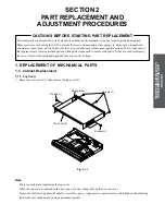
1. Remove seven screws (1), then remove the top cover (2).
Fig. 2-1-1
SECTION
2
P
ART
REPLACEMENT
AND
ADJUSTMENT
PROCEDURES
Screws (1)
Screws (1)
Rating label
Screws (1)
Top cover (2)
SECTION 2
PART REPLACEMENT AND
ADJUSTMENT PROCEDURES
CAUTIONS BEFORE STARTING PART REPLACEMENT
Electronic parts are susceptible to static electricity and may easily damaged, so do not forget to ground as required.
Many screws are used inside the unit. To prevent the screws from missing or dropping, etc. always use a magnetized
screwdriver in servicing. Several kinds of screws are used and some of them need special cautions. That is, take care of
the tapping screws securing molded parts and fine pitch screws used to secure metal parts. If they are used improperly,
the screw holes will be easily damaged and the parts can not be fixed.
1. REPLACEMENT OF MECHANICAL PARTS
Note:
There is a rating label applied on the top cover.
When the top cover is replaced with a new one, put a new rating label on the new top cover.
Transcribe the following items (Model No., serial No., power supply/power requirement etc.) described on the old rating
label to the new rating label by using a permanent marker.
Summary of Contents for RD-XS34SB
Page 30: ...1 1 SHIBAURA 1 CHOME MINATO KU TOKYO 105 8001 JAPAN ...
Page 60: ...1 1 SHIBAURA 1 CHOME MINATO KU TOKYO 105 8001 JAPAN ...
Page 67: ...1 3 4 A B C D E G 2 5 F 4 2 Front Circuit Diagram 4 2 1 Front Jack Circuit Diagram Fig 3 4 2 ...
Page 68: ...10 1 3 4 A B C D E G 2 5 6 7 8 9 F Fig 3 4 3 4 2 2 Front Circuit Diagram L R ...
Page 69: ...Fig 3 4 4 4 3 Digital Circuit Diagram 4 3 1 Digital 1 Circuit Diagram ...
Page 70: ...4 3 Digital Circuit Diagram 4 3 1 Digital 1 Circuit Diagram ...
Page 71: ......
Page 72: ......
Page 73: ......
Page 74: ......
Page 75: ......
Page 76: ......
Page 77: ...Fig 3 4 4 ...
Page 78: ...Fig 3 4 5 4 3 2 Digital 2 Circuit Diagram ...
Page 79: ...4 3 2 Digital 2 Circuit Diagram ...
Page 80: ......
Page 81: ......
Page 82: ......
Page 83: ......
Page 84: ...Fig 3 4 5 ...
Page 86: ...10 1 3 4 A B C D E G 2 5 6 7 8 9 F 4 4 2 Timer Circuit Diagram Fig 3 4 7 ...
Page 89: ...10 1 3 4 A B C D E G 2 5 6 7 8 9 F Fig 3 4 10 4 4 5 MSP Circuit Diagram ...
Page 90: ...1 3 4 A B C D E G 2 5 F 4 5 Tuner Unit Circuit Diagram Fig 3 4 11 ...
Page 95: ...1 2 3 4 5 6 7 A B C D E F 5 6 Mother PC Board Fig 3 5 11 EU05 Mother PC Board Top side ...