1-2-5. Front (R), Front (L) and Front (Jack) PC Boards
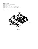
1. Remove the front panel. (Refer to item 1-1-3.)
2. Peel off two tapes (1).
3. Remove four screws (2), then remove the stay (3).
4. Remove four screws (4), then remove the Front (R) PC board (5).
5. Remove two screws (6), then remove the Front (Jack) PC board (7).
6. Remove four screws (8), then remove the Front (L) PC board (9).
Note:
• After replacing, attach the tape (1) to its original position.
Fig. 2-1-11
Screws (2)
Screws (4)
Tapes (1)
Screws (8)
Screws (6)
Stay (3)
Front (L)
PC board (9)
Front (R)
PC board (5)
Front panel
Front (Jack)
PC board (7)
Stay
Wire
Tray door
Front (L)
PC board
Front (R)
PC board
Front (Jack)
PC board
Fasten with the tape.
Fig. 2-1-12
Note:
• Fasten with the tape, taking care so that the wire does not hang over the tray door.
Summary of Contents for RD-XS34SB
Page 30: ...1 1 SHIBAURA 1 CHOME MINATO KU TOKYO 105 8001 JAPAN ...
Page 60: ...1 1 SHIBAURA 1 CHOME MINATO KU TOKYO 105 8001 JAPAN ...
Page 67: ...1 3 4 A B C D E G 2 5 F 4 2 Front Circuit Diagram 4 2 1 Front Jack Circuit Diagram Fig 3 4 2 ...
Page 68: ...10 1 3 4 A B C D E G 2 5 6 7 8 9 F Fig 3 4 3 4 2 2 Front Circuit Diagram L R ...
Page 69: ...Fig 3 4 4 4 3 Digital Circuit Diagram 4 3 1 Digital 1 Circuit Diagram ...
Page 70: ...4 3 Digital Circuit Diagram 4 3 1 Digital 1 Circuit Diagram ...
Page 71: ......
Page 72: ......
Page 73: ......
Page 74: ......
Page 75: ......
Page 76: ......
Page 77: ...Fig 3 4 4 ...
Page 78: ...Fig 3 4 5 4 3 2 Digital 2 Circuit Diagram ...
Page 79: ...4 3 2 Digital 2 Circuit Diagram ...
Page 80: ......
Page 81: ......
Page 82: ......
Page 83: ......
Page 84: ...Fig 3 4 5 ...
Page 86: ...10 1 3 4 A B C D E G 2 5 6 7 8 9 F 4 4 2 Timer Circuit Diagram Fig 3 4 7 ...
Page 89: ...10 1 3 4 A B C D E G 2 5 6 7 8 9 F Fig 3 4 10 4 4 5 MSP Circuit Diagram ...
Page 90: ...1 3 4 A B C D E G 2 5 F 4 5 Tuner Unit Circuit Diagram Fig 3 4 11 ...
Page 95: ...1 2 3 4 5 6 7 A B C D E F 5 6 Mother PC Board Fig 3 5 11 EU05 Mother PC Board Top side ...


