


www.ti.com
Bench Test Setup Conditions
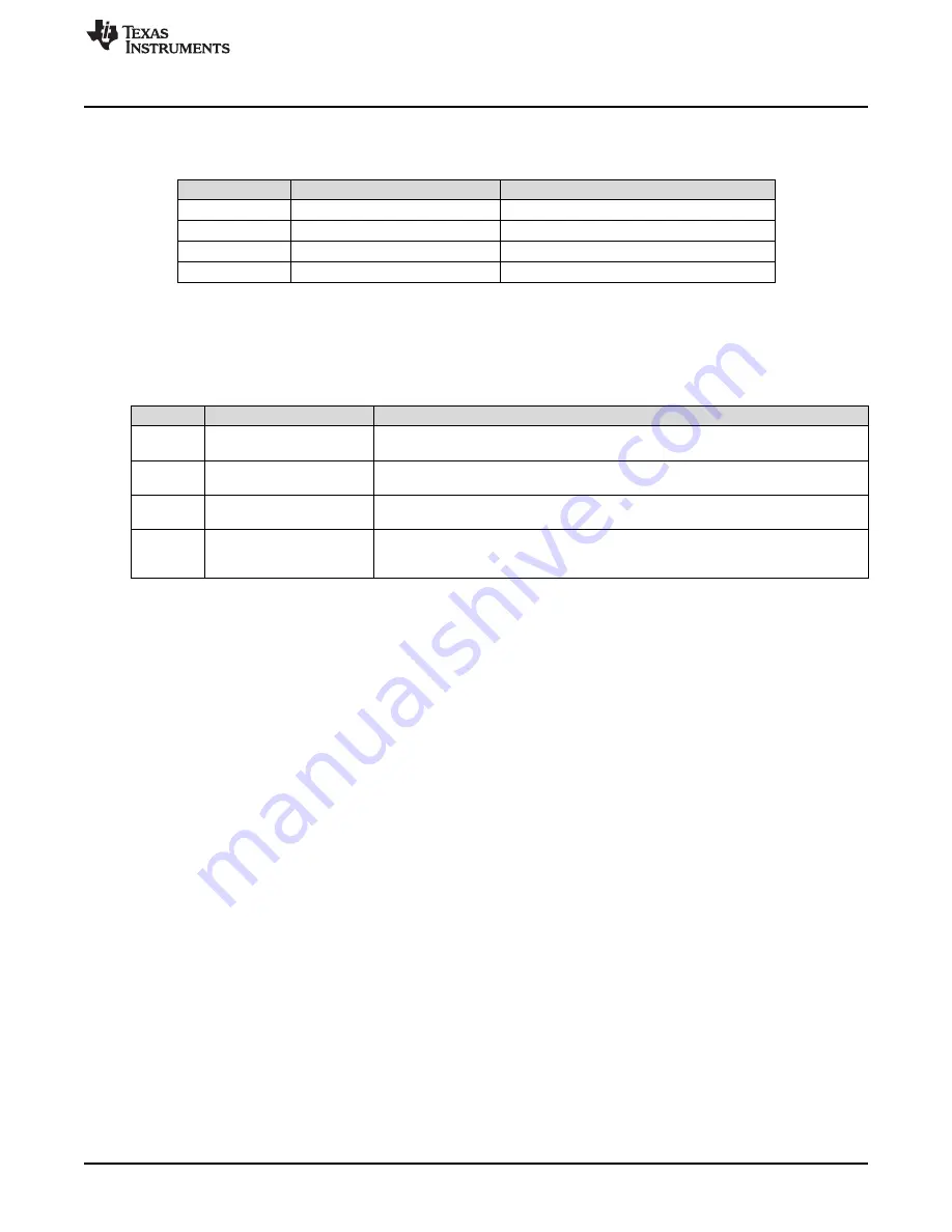
Table 2
lists the I/O connections.
Table 2. Input/Output Connection
Number
Function
Description
J1
BUCK1 connector
Output of BUCK1
J2
BUCK2 connector
Output of BUCK2
J3
BUCK3 connector
Output of BUCK3
J4
VIN connector
Apply power supply to this connector
4.2
Jumpers and Switches
Table 3
lists the jumpers on the EVM.
Table 3. Jumpers
Jumper
Function
Placement
J5
Buck1 enable (EN1)
Connect EN1 to GND to disable VOUT1, connect EN1 to VIN through a 100-k
Ω
resistor to enable VOUT1; leave open to enable VOUT1
J6
Buck2 enable (EN2)
Connect EN2 to GND to disable VOUT2, connect EN2 to VIN through a 100-k
Ω
resistor to enable VOUT2; leave open to enable VOUT2
J7
Buck3 enable (EN3)
Connect EN3 to GND to disable VOUT3, connect EN3 to VIN through a 100-k
Ω
resistor to enable VOUT3; leave open to enable VOUT3
J8
Mode
Power sequencing mode control pin. Connect this pin to GND to set power sequence
with dedicated enable pin; connect this pin to V7V, set the power sequence with the
pre-defined power up and power down sequence.
5
Power-Up Procedure
Power sequence with dedicated enable pin:
1. Connect J8 to GND
2. Apply 4.5 V - 18 V to J4
3. Toggle J5, J6, or J7 to enable VOUT1, VOUT2, and VOUT3, respectively
4. Apply loads to the output connectors
Power sequence with the pre-defined power up and power down sequence:
1. Connect J8 to V7V
2. Connect J5 to High (or Low), J6 to High (or Low)
3. Apply 4.5 V - 18 V to J4
4. Toggle J7 to enable VOUT1, VOUT2, and VOUT3
5. Apply loads to the output connectors.
7
SLVUA85 – June 2014
TPS65261EVM-650 PMIC 3-A, 2-A, 2-A Output Current Evaluation Module
Submit Documentation Feedback
Copyright © 2014, Texas Instruments Incorporated