Quick Setup Guide
www.ti.com
12
SNVU472A – October 2016 – Revised February 2017
Submit Documentation Feedback
Copyright © 2016–2017, Texas Instruments Incorporated
The LP8756xQ1EVM Evaluation Module
2.3
Notes on Efficiency Measurement Procedure
Output Connections: An appropriate electronic load or high-power system source meter instrument,
specified for operation down to 500 mV, is desirable for loading the UUT. The maximum load current is
specified as 4 A per phase. Be sure to choose the correct wire size when attaching the electronic load. A
wire resistance that is too high will cause a voltage drop in the power distribution path which becomes
significant compared to the absolute value of the output voltage. Connect an electric load to X7, X8, X9
and/or X10. It is advised that, prior to connecting the load, it be set to sink 0 A to avoid power surges or
possible shocks.
Voltage drop across the PCB traces will yield inaccurate efficiency measurements. For the most accurate
voltage measurement at the EVM, use TP7 to measure the input voltage and X2 to measure the output
voltage.
To measure the current flowing to/from the UUT, use the current meter of the DC power supply/electric
load as long as it is accurate. Some power source ammeters may show offset of several milliamps and
thus will yield inaccurate efficiency measurements. In order to perform very accurate I
q
measurements on
the UUT, disconnect input protective Zener diode D1 by removing the shunt J3 from the board. When
connected, this diode will cause some leakage, especially on high VIN voltages.
3
GUI Overview
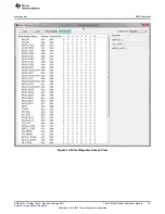
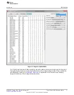
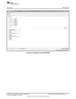
The evaluation software has the following tabs: Main, Config, and Advanced. The three tabs together
provide the user access to the whole register map of the LP8756x. Additional register control can be
obtained from Tools --> Direct Register Access.
3.1
Main Tab
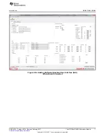
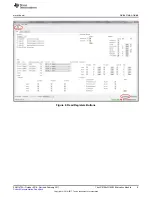
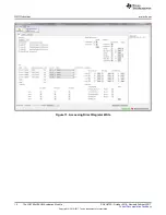
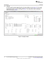
The Main tab (see for example
Figure 10
) has the elemental controls for the EVM and provides a view to
the chip status. Starting from top, the main controls are:
•
I2C mode or 4 Enable mode. If this states I2C mode, device is controlled with I2C. When this states
4EN mode, bucks are controlled with ENx pins.
•
Assert NRST: This checkbox will assert high level to LP8756xQ1 NRST pin. This pin enables the chip
internal voltage reference and bias circuitry.
•
Assert EN1: This checkbox will assert high level to LP8756xQ1 EN1 pin. Asserting EN1 may enable
the buck regulator(s) or switch to different output voltage level, depending on the register settings.
•
Assert EN2: This checkbox will assert high level to LP8756xQ1 EN2 pin. Asserting EN2 may enable
the buck regulator(s) or switch to different output voltage level, depending on the register settings.
•
Assert EN3: This checkbox will assert high level to LP8756xQ1 EN3 pin. Asserting EN3 may enable
the buck regulator(s) or switch to different output voltage level, depending on the register settings.
•
Assert EN4: In 4 Enable mode, this checkbox will assert high level to LP8756x SCL pin, (alternative
function is EN4). Asserting EN4 may enable the buck regulator(s), depending on the register settings.
This checkbox is visible only when device is configured to 4 Enable Signal Mode.
•
Assert SW Reset: To perform a complete SW reset to the chip, assert this checkbox. See the
LP8756
datasheet
for explanation of LP8756 reset scenarios.
NOTE:
The recommended start-up sequence for LP8756xQ1 is to first assert NRST, then write all
needed configuration bits by using the GUI, and then enable buck regulator(s) by ENx pin or
EN_BUCKx bit.


