background image

Copyright © 2017, Texas Instruments Incorporated

KCU105 Quick Start-Up Instructions

www.ti.com

8

SLAU711 – March 2017

Submit Documentation Feedback

Copyright © 2017, Texas Instruments Incorporated

HSDC Pro With Xilinx

®

KCU105

6.3

Adjusting FPGA FMC Settings

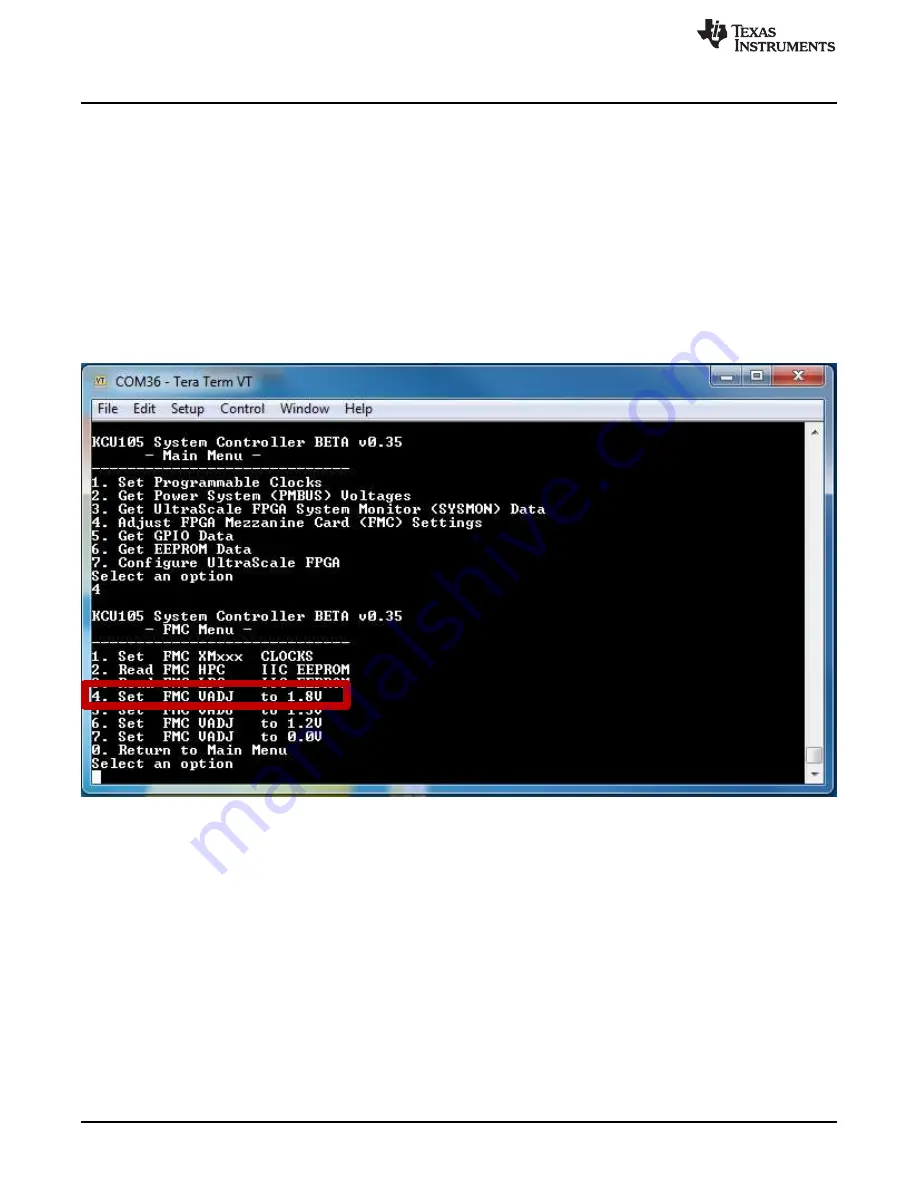
The FMC VADJ voltage must be set to 1.8V in order for the platform to work. This is set in the Enhanced
COM Port terminal.

1. Navigate to the Enhanced COM Port window. Return to the main menu by entering "0" in the terminal.

2. Enter

4

to "Adjust FPGA Mezzanine Card (FMC) settings".

3. Enter

4

again to "Set FMC VADJ to 1.8V".

4. Enter

0

to return to the main menu.

5. To check this voltage, enter

2

to "Get the Power Systems Voltages".

6. Enter

7

to "Get VADJ1D8 voltage". The voltage should appear above the menu.

7. Enter

0

to return to the main menu.

Figure 3

highlights setting the FMC VADJ to 1.8V in the Enhanced COM Port terminal.

Figure 3. Setting FMC VADJ in Enhanced COM Port

6.4

IP Address and Connecting to HSDC Pro

Once the firmware has been loaded and the FPGA is programmed, the board IP address and port number
will be available on the Standard COM port, shown in

Figure 4

.

This is required to establish a connection between the KCU105 and HSDC Pro. To connect to HSDC Pro,
do the following steps:

1. Open the HSDC Pro GUI as administrator.

2. In the "Select Board" pop up, check "Connect to KCU105". Enter the IP address followed by a colon

and port number. There is also an option to select from the drop-down menu. Both IP address and port
number can be found in the Standard COM port terminal.

3. Press "OK" to connect to the KCU105.

Summary of Contents for KCU105

Page 1: ...nd Drivers 6 6 2 Programing the FPGA 7 6 3 Adjusting FPGA FMC Settings 8 6 4 IP Address and Connecting to HSDC Pro 8 7 Board Setup Examples 10 7 1 DAC38J84EVM with KCU105 Board Setup Example 10 7 2 ADC12J4000EVM With KCU105 Board Setup Example 15 7 3 ADC32RF45EVM With KCU105 Board Setup Example 18 7 4 ADS54J20EVM With KCU105 Board Setup Example 22 7 5 ADS42JB49EVM With KCU105 Board Setup Example 2...

Page 2: ...p With KCU105 27 26 DAC38RFXX EVM GUI in External Clock Mode 28 27 DAC38RF82EVM GUI DCLK Divider 29 28 Generating a 150 MHz Tone on HSDC Pro 29 29 Analog Output From DAC38RF82EVM 30 30 DAC38RFXX EVM GUI in PLL Mode 31 31 DAC38RF82EVM GUI NCO Frequency Settings 32 32 HSDC Pro Configuration for PLL Mode 33 33 Analog Output From DAC38RF82EVM 34 34 Eye Diagram Example Plot 35 List of Tables 1 Multipli...

Page 3: ... designed for this integration is used to support HSDC Pro communication through SPI and any TI FMC based JESD204B EVM at any line rate This user s guide is a starting point but the firmware is over complicated for designing a regular system The firmware is located at the following Xilinx web site https www xilinx com member jesd204_eval uhwd_2016_3_v1_0 zip The zip file includes documentation of ...

Page 4: ...nverter EVMs or JESD204B interface modes become available that are not currently supported by the latest release of HSDC Pro GUI the HSDCProv_xpxx_Patch_setup executable available on the TI website under the High Speed Data Converter Pro Software product folder http www ti com tool dataconverterpro sw will allow the user to add these to the GUI device list After the patch has been downloaded follo...

Page 5: ...ne rates and subclasses with a single programmable design The Xilinx IP used in the firmware can be driven by a single clock in many circumstances see the clocking section of the Xilinx IP product guide for more details THE REFCLK and core clock are determined by the line rate conditions shown in Table 1 Table 1 Multiplier Line Rate Ranges Max Lr Gbps 1 2 1 6 1 9 2 2 4 3 2 3 9 4 4 9 6 5 7 9 8 1 8 ...

Page 6: ... to JTAG interface J1 and the other between the dual USB UART port J4 Ensure that Silicon Labs drivers are installed See the KCU105 user guide on Xilinx com for details about the Silicon Labs CP2105GM dual USB to UART Bridge interface on the KCU105 4 Connect a USB cable between the EVM and host computer 5 Open a serial port connection with any serial terminal emulator 6 Initialize a serial port co...

Page 7: ...k on Finish 6 Click on Program device located on the green bar Select xcku040_0 also at Tools Program device 7 Select the proper bit stream file The firmware is found in C Program Files x86 Texas Instruments High Speed Data Converter Pro KCU105 Details Firmware KCU105_TI_DHCP bit NOTE If there is an error regarding ASCII characters drag the bit file to the desktop and target the file there 8 Click...

Page 8: ...o Get VADJ1D8 voltage The voltage should appear above the menu 7 Enter 0 to return to the main menu Figure 3 highlights setting the FMC VADJ to 1 8V in the Enhanced COM Port terminal Figure 3 Setting FMC VADJ in Enhanced COM Port 6 4 IP Address and Connecting to HSDC Pro Once the firmware has been loaded and the FPGA is programmed the board IP address and port number will be available on the Stand...

Page 9: ...m KCU105 Quick Start Up Instructions 9 SLAU711 March 2017 Submit Documentation Feedback Copyright 2017 Texas Instruments Incorporated HSDC Pro With Xilinx KCU105 Figure 4 IP Address in Standard COM Port Figure 5 is a screenshot of HSDC Pro connecting to the KCU105 Figure 5 HSDC Pro Connecting to KCU105 ...

Page 10: ...t needs to be modified in order for the integration to work The instructions in Section 6 must be completed before continuing with the following examples 7 1 DAC38J84EVM with KCU105 Board Setup Example The following section provides an example of testing the DAC38J84EVM using a KCU105 development platform With the updated firmware users can use the DAC38J84 GUI as if it was connected to TI s TSW14...

Page 11: ... done in the following a EVM Clocking Mode Onboard b DAC Data Input Rate 1228 8 MSPS c Number of SerDes Lanes per DAC 8 d Interpolation 2 Figure 7 is a screenshot of a configured GUI for a DAC38J84EVM 8411 JESD204B mode Figure 7 DAC38J84EVM GUI Configuration 3 Press the 1 Program LMK04828 and DAC3XJ8X button 4 Open HSDC Pro press on the DAC tab and select DAX3XJ84_LMF_841 from the drop down menu 5...

Page 12: ...e 8 Generating a Tone With HSDC Pro GUI 6 Click the Create Tones button and press the Send button 7 The new lane rate 12 288 GHz and FPGA Clock 307 2 MHz settings should be shown 8 Go back to the DAC38J84 GUI and press 2 Reset DAC JESD Core and 3 Trigger LMK04828 SYSREF 9 Connect channel one of the DAC38J84EVM to a spectrum analyzer and verify the signal Figure 9 shows the analog output generated ...

Page 13: ...rated HSDC Pro With Xilinx KCU105 7 1 1 DAC38J84EVM Second Example In this example the same mode is used but a different configuration that shows the limitations of the KCU105 1 Configure the GUI as shown in Figure 10 a EVM Clocking Mode Onboard b DAC Data Input Rate 368 64 MSPS c Number of SerDes Lanes per DAC 8 d Interpolation 4 Figure 10 DAC38J84EVM GUI Configuration ...

Page 14: ...own to be 3 6G the valid Multiplier line rate is only supported by x10 and x20 refer to Table 1 In order to support this mode the settings of the LMK04828 registers needs to be changed From the GUI navigate to the LMK04828 Controls tab Under Clock Outputs update the DCLK Divider to 16 in the DAC GUI as shown in Figure 11 Figure 11 DAC38J84EVM GUI DCLK Divider Follow the procedure in Section 7 1 be...

Page 15: ...ode using a KCU105 development platform NOTE There is a jumper KC705 JTAG on the ADC12J4000EVM that will prevent the firmware from downloading if it is not shunted By default the board will have this jumper OPEN The jumper is required to be shunted in order for this integration to work The jumper is located on the top of the board near the FMC connector Make sure the instructions in Section 6 are ...

Page 16: ...follows 1 Connect the power supply cables and power up the ADC12J400 2 Open the ADC12J4000 GUI The GUI is found under Software on www ti com featuring the ADC12J4000EVM 3 Choose On board as the Clock Source set On board Fs Selection to Fs 4000 Msps and set Decimation and Serial Data Mode to Bypass Mode DDR 4 Click Program Clocks and ADC Figure 13 shows a screenshot of the configured GUI Figure 13 ...

Page 17: ...HSDC Pro select the ADC tab and select ADC12J4000_BYPASS using the device drop down menu 6 Enter 4G in the ADC Output Data Rate window Verify the number of samples do not exceed 32 768 7 Click the Capture button and the new line rate 8G and JESD reference clock 200M should show Figure 14 shows a captured result sending a 170 MHz single tone through Vin at 1 dBFS Figure 14 HSDC Pro ADC12J4000EVM Ca...

Page 18: ...d HSDC Pro With Xilinx KCU105 7 3 ADC32RF45EVM With KCU105 Board Setup Example The following section provides an example testing the ADC32RF45EVM in 8224 mode using an external clock in Bypass mode Make sure the instructions in Section 6 are completed before testing the EVM Figure 15 shows a setup between the ADC32RF45EVM and KCU105 Figure 15 ADC32RF45EVM Setup With KCU105 ...

Page 19: ..._CLKIN J7 of the ADC32RF45EVM This source must be synchronized with the ADC_CLK_IN source 3 Connect the power supply cable to the EVM and open the ADC32RFxx EVM GUI The GUI is found under Software on www ti com featuring the ADC32RF45EVM 4 Go to the Quick Setup tab and configure the GUI as shown in Figure 16 a Clock Source to ADC External Clocking b ADC32RF45 Mode Bypass c BYPASS 14 bit Figure 16 ...

Page 20: ...eedback Copyright 2017 Texas Instruments Incorporated HSDC Pro With Xilinx KCU105 Figure 17 ADC32RFEVM GUI Clock Outputs 8 Click on the SYSREF and SYNC tab Verify the SYSREF Divider is set to 1024 9 In the ADC Configuration tab under ADC32RFxx set the JESD204b Lane De emphasis setting to 0 dB for all lanes as shown in Figure 18 Figure 18 ADC32RF45 GUI Lane De Emphasis ...

Page 21: ...Open HSDC Pro select the ADC tab and select ADC32RF34_8224 using the drop down menu 11 Enter 2G for ADC Output Data Rate the new lane rate 10G and reference clock settings 200M will be shown Verify the number of samples do not exceed 32 768 12 Click the Capture button Figure 19 shows a captured result sending a 170 MHz single tone through Vin at 2 dBFS to AINP J2 Figure 19 ADC32RF45EVM Capture on ...

Page 22: ... Example The following section provides an example testing the ADS54J20EVM in 8224 mode with the KCU105 development platform EVMs in the same family such as the ADS54J40EVM and ADS54J60EVM can be configured with the same instructions and proper configuration files Make sure the instructions in Section 6 are completed before testing the EVM Figure 20 shows a setup between the ADS54J20EVM and the KC...

Page 23: ...DS54JxxEVM GUI The GUI is found under Software on www ti com featuring the ADS54J20EVM 2 Navigate to the LMK04828 tab and click the RESET button 3 On the Low Level View tab load the following configuration files LMK_983p04_8224_VC707 cfg as shown in Figure 21 Figure 21 Configuration Files for ADS54J20EVM GUI 4 Press the ADC RESET button SW1 on the EVM to provide a hardware reset to the ADC 5 On th...

Page 24: ...S54J20_LMF_8224 in the drop down arrow 7 Verify the number of samples do not exceed 32 768 Enter 983 04M in the ADC Output Data Rate window 8 The GUI will display the new lane rate 4 9152G and JESD reference clock required by the capture platform FPGA 245 76M 9 Click on OK Click the Capture button Figure 22 shows a captured result sending a 170 MHz single tone through Vin at 1 dBFS Figure 22 HSDC ...

Page 25: ...tructions and proper configuration files Make sure the instructions in Section 6 are completed before testing the EVM Figure 23 shows a setup between the ADS42JB49EVM and the KCU105 Figure 23 ADS42JB49EVM Setup With KCU105 Set up the hardware as follows 1 Connect the power cable to the ADS42JB49EVM and open the ADS42JBXX GUI The GUI is found under Software on www ti com featuring the ADS42JB69EVM ...

Page 26: ...1 using the device drop down menu 6 Verify the number of samples do not exceed 32 768 7 Enter 250M in the ADC Output Data Rate window The GUI will display the new lane rate 2 5G and JESD reference clock required by the capture platform FPGA 250M 8 Click on OK Connect an analog input signal to the SMA connect J1 9 Click the Capture button Figure 24 shows a captured result sending a 80 MHz single to...

Page 27: ...2EVM With KCU105 Board Setup Example The following section provides an example of testing the DAC38RF82EVM using a KCU105 development platform With the updated firmware users can use the DAC38RFXX GUI as if it was connected to a TI TSW14J56 Make sure the instructions in Section 6 are completed before testing the EVM Figure 25 shows a setup between the DAC38J84EVM and KCU105 Figure 25 DAC38RF82EVM ...

Page 28: ...ernal clock mode 3 Connect a power cable to the DAC38RF82EVM and open the DAC38RFXX GUI The GUI is found under Software on www ti com featuring the DAC38RF82EVM 4 On the Quick Start tab toggle DAC RESETB Pin and press the Load Default button 5 Configure the GUI as shown in Figure 26 a DAC Clock Frequency MHz 6000 b of DACs Dual DAC c of IQ pairs per DAC 1 IQ pair d of serdes lanes per DAC 4 Lanes ...

Page 29: ...ated HSDC Pro With Xilinx KCU105 Figure 27 DAC38RF82EVM GUI DCLK Divider 8 Open HSDC Pro press the DAC tab and select DAX38RF8X_LMF_841 from the drop down menu 9 Enter 375M as the Data Rate SPS and change the DAC Option to 2 s Complement Make sure the number of samples is set to at least 8192 but do not exceed 32 768 Figure 28 shows a configured GUI for a 150 MHz tone Figure 28 Generating a 150 MH...

Page 30: ... the Create Tones button and press the Send button 11 The new lane rate 3 750 GHz and FPGA Clock 375 MHz settings should be shown 12 Go back to the DAC38RFXX GUI and press the Reset DAC JESD Core SYSREF TRIGGER button 13 Connect channel one of the DAC38RF82EVM J6 to a spectrum analyzer and verify the signal Figure 29 shows the analog output generated by the DAC38RF82EVM Figure 29 Analog Output Fro...

Page 31: ...generator to EVM LMK CLKIN J4 of the DAC38RF82EVM 2 Verify that the jumper labeled JP10 is OPEN 3 Connect a power cable to the DAC38RF82EVM and open the DAC38RFXX GUI The GUI is found under Software on www ti com featuring the DAC38RF82EVM 4 On the Quick Start tab toggle the DAC RESETB Pin and press the Load Default button 5 Configure the GUI as shown in Figure 30 a PLL Enable Check b M 9 N 1 c Re...

Page 32: ...gate to the DAC38RF8x tab Under Digital DAC A enable the Mixer and NCO as shown in Figure 31 Set the Mixer Gain to 6dB and the NCO Frequency MHz to 1960 8 Click the UPDATE NCO button Go back to the Quick Start tab and press Reset DAC JESD Core SYSREF TRIGGER button This can also be done on the Digital DAC B tab which will provide an NCO Frequency on channel B Figure 31 DAC38RF82EVM GUI NCO Frequen...

Page 33: ...and change DAC Option to 2 s Complement Make sure the number of samples is set to at least 8192 but no more than 32 768 11 Set the following in the I Q Multitone Generator a Tone BW 1 b of Tones 1 c Tone Center 0 This will change to the closest value possible to DC d Tone selection Complex Figure 32 is a screenshot of a proper configuration on HSDC Pro Figure 32 HSDC Pro Configuration for PLL Mode...

Page 34: ...7 Texas Instruments Incorporated HSDC Pro With Xilinx KCU105 14 Go back to the DAC38RFXX GUI and press the Reset DAC JESD Core SYSREF TRIGGER button 15 Connect channel one of the DAC38RF82EVM J6 to a spectrum analyzer and verify the signal Figure 33 shows the analog output generated by the DAC38RF82EVM Figure 33 Analog Output From DAC38RF82EVM ...

Page 35: ...In HSDC Pro under the Instrument Options tab click on SERDES Test Options 3 A new window should appear with the following features a Lane Selects one of the lanes to analyze the lane number is respective to the KCU105 b Horz Step Resolution of the horizontal scan For optimal resolution choose 4 or lower c Vert Step Resolution of the vertical scan For optimal resolution choose 4 or lower d Max Pres...

Page 36: ...y set forth above or credit User s account for such EVM TI s liability under this warranty shall be limited to EVMs that are returned during the warranty period to the address designated by TI and that are determined by TI not to conform to such warranty If TI elects to repair or replace such EVM TI shall have a reasonable time to repair such EVM or provide replacements Repaired EVMs shall be warr...

Page 37: ...the user guide with the maximum permissible gain and required antenna impedance for each antenna type indicated Antenna types not included in this list having a gain greater than the maximum gain indicated for that type are strictly prohibited for use with this device Concernant les EVMs avec antennes détachables Conformément à la réglementation d Industrie Canada le présent émetteur radio peut fo...

Page 38: ...ed loads Any loads applied outside of the specified output range may also result in unintended and or inaccurate operation and or possible permanent damage to the EVM and or interface electronics Please consult the EVM user guide prior to connecting any load to the EVM output If there is uncertainty as to the load specification please contact a TI field representative During normal operation even ...

Page 39: ...COST OF REMOVAL OR REINSTALLATION ANCILLARY COSTS TO THE PROCUREMENT OF SUBSTITUTE GOODS OR SERVICES RETESTING OUTSIDE COMPUTER TIME LABOR COSTS LOSS OF GOODWILL LOSS OF PROFITS LOSS OF SAVINGS LOSS OF USE LOSS OF DATA OR BUSINESS INTERRUPTION NO CLAIM SUIT OR ACTION SHALL BE BROUGHT AGAINST TI MORE THAN TWELVE 12 MONTHS AFTER THE EVENT THAT GAVE RISE TO THE CAUSE OF ACTION HAS OCCURRED 8 2 Specif...

Page 40: ... TI Resource NO OTHER LICENSE EXPRESS OR IMPLIED BY ESTOPPEL OR OTHERWISE TO ANY OTHER TI INTELLECTUAL PROPERTY RIGHT AND NO LICENSE TO ANY TECHNOLOGY OR INTELLECTUAL PROPERTY RIGHT OF TI OR ANY THIRD PARTY IS GRANTED HEREIN including but not limited to any patent right copyright mask work right or other intellectual property right relating to any combination machine or process in which TI product...

Reviews: