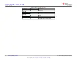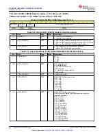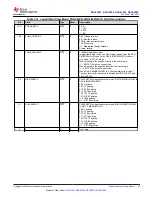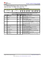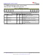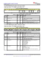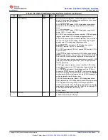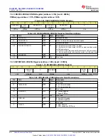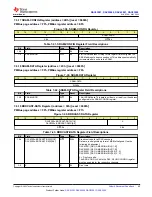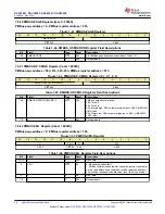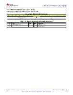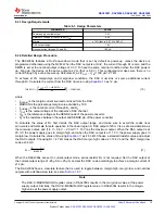
Table 7-38. GPIO-CONFIG Register Field Descriptions (continued)
Bit
Field
Type
Reset
Description
4-1
GPI-CONFIG
R/W
0000
GPIO pin input configuration. Global settings act on the entire
device. Channel-specific settings are dependent on the channel
selection by the GPI-CH-SEL bits:
0000: DEEP-SLEEP (global). GPIO falling edge triggers deep-
sleep mode, GPIO rising edge brings the device out of deep-
sleep.
0010: FAULT-DUMP (global). GPIO falling edge triggers fault
dump, GPIO = 1 has no effect.
0011: IOUT power up-down (channel-specific). GPIO falling edge
triggers power down, GPIO rising edge triggers power up.
0100: VOUT power up-down (channel-specific). The output load
is as per the VOUT-PDN-X setting. GPIO falling edge triggers
power down, GPIO rising edge triggers power up.
0101: PROTECT input (global). GPIO falling edge asserts
PROTECT function, GPIO = 1 has no effect.
0111: CLR input (global). GPIO = 0 asserts CLR function, GPIO =
1 has no effect.
1000: LDAC input (channel-specific). GPIO falling edge asserts
LDAC function, GPIO = 1 has no effect. Both the SYNC-CONFIG-
X and the GPI-CH-SEL must be configured for every channel.
1001: Start and stop function generation (channel-specific). GPIO
falling edge stops function generation. GPIO rising edge starts
function generation.
1010: Trigger margin high-low (channel-specific). GPIO falling
edge triggers margin low. GPIO rising edge triggers margin high.
1011: RESET input (global). The falling edge of the GPIO pin
asserts the RESET function. The RESET input must be a pulse.
The GPIO rising edge brings the device out of reset. The RESET
configuration must be programmed into the NVM. Otherwise the
setting is cleared after the device reset.
1100: NVM write protection (global). GPIO falling edge allows
NVM programming. GPIO rising edge blocks NVM programming.
1101: Register-map lock (global). GPIO falling edge allows
update to the register map. GPIO rising edge blocks any register
map update except a write to the DEV-UNLOCK field through I
2
C
or SPI and to the RESET field through I
2
C.
Others: Invalid
0
GPI-EN
R/W
0
0: Disable input mode for GPIO pin.
1: Enable input mode for GPIO pin.
DAC53001, DAC53002, DAC63001, DAC63002
SLASF48 – MAY 2022
Copyright © 2022 Texas Instruments Incorporated
67
Product Folder Links:


