C5535 DSPShield H/W Reference Manual
Version 0.1
In Collaboration with Stanford University
page
9
the RTC can be the reference source for the C5535 DSP’s system clock generator.
Resistors R8, R9, R10 and R59 select the source as shown in Table 6. The different
clocks within the system clock generator block can be output on the C5535 DSP’s
CLKOUT pin and monitored at Test Point TP1.
System Clock Generator
Reference Source
Resistor Select
12MHz External Oscillator
(Default)
R8=DNI, R9=10K Ohm, R10=DNI, R59=0 Ohm
32.768 RTC
R8=0 Ohm, R9=DNI, R10=0 Ohm, R59=DNI
Table 6. System Clock Generator Reference Source Select
3.3 ROM Bootloader
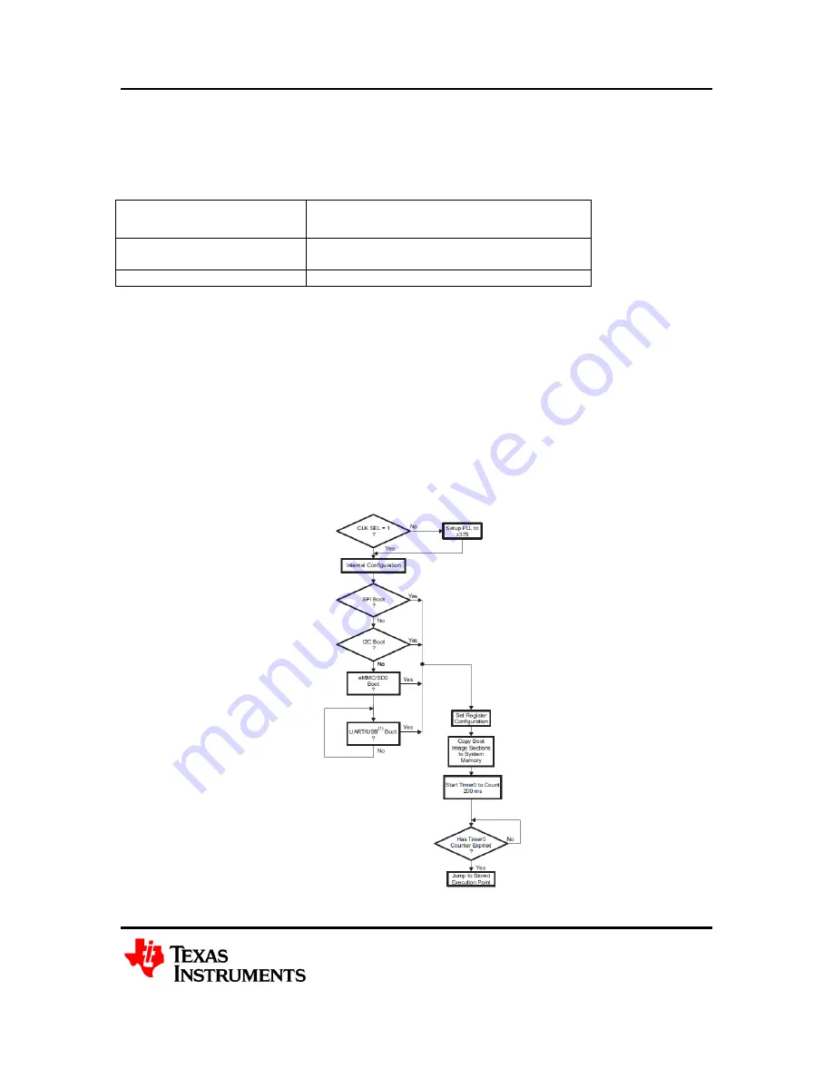
The C5535 DSP has an on-chip ROM Bootloader (RBL). It samples the following
interfaces, in order, looking for a boot signature: SPI EEPROM, I2C EEPROM,
MMC/SD0 AND UART/USB. Once a boot signature is detected, the C5535 DSP will
download the boot image and then jump to the entry point specified in the image. For the
DSPShield, the SD0 peripheral connected to the micro SD Card connector is the default
boot source. Figure 4 shows the Bootloader Software Architecture (from the C5535 DSP
datasheet). In the case where no boot source is found, the LED_XF will remain lit.
Figure 4. Bootloader Software Architecture


