background image

INB

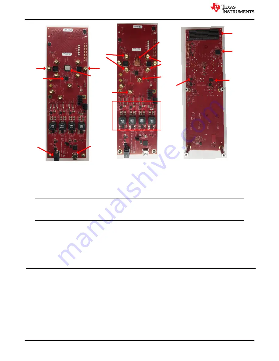
( J7 )

ADC12DJ5200RF

ADC12DJ5200RF EVM top side 

without heat sink installed

INA

( J4 )

USB 

Connector

+12V DC

ADC12DJ5200RF EVM top side with 

heat sink installed

Power (DC/DC


DQG /'2¶V

)

External device

Clock input ( J10 )

INB+/-

INA+/-

External reference

clock input ( J17 )

FMC+

connector

LMK04828

LMK61E2

ADC12DJ5200RF EVM bottom side

LM95233

Heat Sink for the ADC

Copyright © 2016, Texas Instruments Incorporated

LMX2594

Figure 1-1. EVM Orientation

The digital data from the ADCxxDJxx00RFEVM board is quickly and easily captured with the TSW14J57EVM 
data capture boards.

Note

The TSW14J57EVM cannot be used for JMODES that use 64b/66b encoding, or serial rates above 15 
Gbps.

The TSW14J57EVM captures the high-speed serial data, decodes the data, stores the data in memory, and then 
uploads it to a connected PC through a USB interface for analysis. The High-Speed Data Converter Pro (HSDC 
Pro) software on the PC communicates with the hardware and processes the data.

With proper hardware selection in the HSDC Pro software, the TSW14J57 device is automatically configured to 
support a wide range of operating speeds of the ADCxxDJxx00RFEVM, but the device may not cover the full 
operating range of the ADC device. Serial data rates of 15 Gbps down to 1 Gbps are supported.

www.ti.com

2

ADCxxDJxx00RF Evaluation Module

SLAU640A – APRIL 2019 – REVISED JUNE 2021

Submit Document Feedback

Copyright © 2021 Texas Instruments Incorporated

Summary of Contents for ADC DJ 00RF Series

Page 1: ...nded signal source from 500 kHz to 9 GHz The LMX2594 clock synthesizer generates the ADC sampling clock The LMK04828 LMK61E2 and LMX2594 onboard system clock generator generates SYSREF and FPGA reference clocks for the high speed serial interface Transformer coupled clock input network to test the ADC performance with an external low noise clock source LM95233 temperature sensor High speed serial ...

Page 2: ...at use 64b 66b encoding or serial rates above 15 Gbps The TSW14J57EVM captures the high speed serial data decodes the data stores the data in memory and then uploads it to a connected PC through a USB interface for analysis The High Speed Data Converter Pro HSDC Pro software on the PC communicates with the hardware and processes the data With proper hardware selection in the HSDC Pro software the ...

Page 3: ...e 7 3 External Reference Clocking System Block Diagram 20 Figure 7 4 External Clock Configuration 21 Figure 7 5 Onboard Clocking Configuration 22 Figure A 1 Analog Input Path 24 Figure A 2 3 dB attenuation pad 25 List of Tables Table 4 1 Supported and Non Supported Features of the JESD204C Device 13 Table 4 2 Low Level Controls 14 Table 5 1 Troubleshooting 15 Table 8 1 ADCxxDJxx00RFEVM Signal Rout...

Page 4: ...ut INA J4 Single Ended Input Mini USB Connector J20 12V DC J14 INB J6 J8 Differential Input INA J3 J5 Differential Input DEVCLK J10 ADC Sampling Clock External Reference Clock J17 Copyright 2016 Texas Instruments Incorporated Figure 2 1 EVM Feature Locations Equipment www ti com 4 ADCxxDJxx00RF Evaluation Module SLAU640A APRIL 2019 REVISED JUNE 2021 Submit Document Feedback Copyright 2021 Texas In...

Page 5: ...an 18 dBm power less than 5 dB insertion loss Trilithic 5VH series tunable BPF K L Microwave BT series tunable BPF TTE KC6 or KC7 series fixed BPF Signal path cables SMA or BNC or both SMA and BNC By default the ADCxxDJxx00RFEVM has an external clocking solution A few small board modifications enable onboard clocking If onboard clocking is used the following equipment is recommended One low noise ...

Page 6: ...ffs provide the proper height for robust connector connections 3 4 Connect the Power Supplies to the Boards Power Off 1 Confirm that the power switch on the TSW14J57EVM is in the off position Connect the power cable to a 12 V DC minimum 3 A power supply Ensure the proper supply polarity by confirming that the outer surface of the barrel connector is GND and the inner portion of the connector is 12...

Page 7: ...260MHz clock frequency Set the output power to approximately 6 9 dBm Note a The Reference clock frequency can be obtained from the ADC12DJ5200RFEVM GUI Once the ADC12DJ5200EVM GUI is configured to the desired JMODE mode and clock rate The Reference Clock frequency required by the EVM is displayed on first page of the GUI shown with red square in Figure 3 2 b Ensure that the DEVCLK and Reference cl...

Page 8: ...e The max clock rate supported by ADC12DJ4000RF is 4000 MHz and only 8 bit mode are suppored by ADC08DJ5200RF All the 12 bit and 15 bit modes are disabled on ADC08DJ5200RF Figure 3 2 Configuration GUI EVM Tab Setup Procedure www ti com 8 ADCxxDJxx00RF Evaluation Module SLAU640A APRIL 2019 REVISED JUNE 2021 Submit Document Feedback Copyright 2021 Texas Instruments Incorporated ...

Page 9: ...s action will overwrite any previous device register settings 6 The Reference frequency required by the EVM is shown under indicator Reference Clock 3 10 Calibrate the ADC Device on the EVM Figure 3 3 Configuration GUI ADC Control 1 With the EVM GUI open on the PC navigate to the Control tab 2 To calibrate the ADC click Cal Triggered Running once then click it again This will stop and re start the...

Page 10: ...e connected to the ADC12DJ5200RFEVM 3 Select the ADC12DJxx00RF_JMODE1 device from the ADC select drop down in the top left corner 4 When prompted click Yes to update the firmware Note If the user configures the EVM with options other than the default register values different instructions may be required for selecting the device in HSDC Pro See Section 7 for more details 5 Enter the ADC Output Dat...

Page 11: ...ADC Input Signal Frequency 3 NCO Frequency 4 Decimation Factor The HSDC Pro GUI will calculate the ADC Output Data Rate based on these inputs The Fundamental and Harmonic frequency locations will also be calculated and identified in the FFT display www ti com Setup Procedure SLAU640A APRIL 2019 REVISED JUNE 2021 Submit Document Feedback ADCxxDJxx00RF Evaluation Module 11 Copyright 2021 Texas Instr...

Page 12: ... Additional Device Parameters Dialog Box Setup Procedure www ti com 12 ADCxxDJxx00RF Evaluation Module SLAU640A APRIL 2019 REVISED JUNE 2021 Submit Document Feedback Copyright 2021 Texas Instruments Incorporated ...

Page 13: ... frames per multiframe K Kmin 3 256 1 Kmax 256 Kstep 1 or 2 Most values of K supported constrained by requirement that K F 4n Most values of K supported constrained by requirement that K F 4n Scrambling Supported Supported Supported Test patterns PRBS7 PRBS9 PRBS15 PBRS23 PRBS31 Ramp Transport Layer test D21 5 K28 5 Repeat ILA Modified RPAT Serial Out 0 Serial Out 1 Clock test ADC Test Pattern 1 I...

Page 14: ...summary Read register button Read from the register highlighted in the Register Map summary and display the results in the Read Data field Can be used to re synchronize the GUI with the state of the hardware Read all button Read from all registers in the Register Map summary and display the current state of the hardware Load Configuration button Load a configuration file from disk and register add...

Page 15: ...If it is not lit click the Reconnect FTDI button Try restarting the configuration GUI Configuration GUI is not able to connect to the EVM Use the free FT_PROG software from FTDI chip and verify that the onboard FTDI chip is programmed with the product description ADC12DJxx00RF HSDC Pro software is not capturing good data or analysis results are incorrect Verify that the TSW14J57EVM is properly con...

Page 16: ...lso available in the help menu of the software LMK04828 data sheet LMX2594 data sheet FTDI USB to Serial Driver Installation Manual www ftdichip com Support Documents InstallGuides htm 6 2 TSW14J57EVM Operation Refer to the TSW14J57EVM user guide for configuration and status information References www ti com 16 ADCxxDJxx00RF Evaluation Module SLAU640A APRIL 2019 REVISED JUNE 2021 Submit Document F...

Page 17: ... frequency must also be programmed to a compatible frequency Ensure that the K value complies with the K Min and Step values for the selected JMODE Refer to the ADC12DJ5200RF operating modes table in the ADC12DJ5200RF data sheet 7 2 Customizing the EVM for Optional Clocking Support The ADC12DJ5200RFEVM can be clocked using 3 different methods external clock option onboard clock option and external...

Page 18: ...e external clocks with the following steps see Figure 7 4 1 Modify the hardware a Remove R171 and R174 populate C2 and C3 b Remove C52 and C306 populate C60 and C61 c Install Jumper J13 SYNC SYSREFREQ OSCIN RFOUTA RFOUTB SDCLKx SDCLKx DCLKx SDCLKx DA 15 0 SYNC FPGA_CLK 3 0 FPGA_SYSREF CLKIN0 CLKIN1 LMK61E2 LMK00304 SDCLKx LMK04828 LMX2594 ADC12DJ5200RF CLK SYSREF DA 15 0 FMC SYNC REFCLK J17 260 MH...

Page 19: ...an be configured to use onboard clocking option with the following steps see Figure 7 5 Remove C2 and C3 populate R171 and R174 Remove C60 and C61 populate C52 and C306 Uninstall Jumper J13 SYNC SYSREFREQ OSCIN RFOUTA RFOUTB SDCLKx SDCLKx DCLKx SDCLKx DA 15 0 SYNC FPGA_CLK 3 0 FPGA_SYSREF CLKIN0 CLKIN1 LMK61E2 LMK00304 SDCLKx LMK04828 LMX2594 ADC12DJ5200RF CLK SYSREF DA 15 0 FMC SYNC Board SYNC On...

Page 20: ...ence clocking option with the following steps see Figure 7 5 Remove C2 and C3 populate R171 and R174 Remove C60 and C61 populate C52 and C306 Install Jumper J13 SYNC SYSREFREQ OSCIN RFOUTA RFOUTB SDCLKx SDCLKx DCLKx SDCLKx DA 15 0 SYNC FPGA_CLK 3 0 FPGA_SYSREF CLKIN0 CLKIN1 LMK61E2 LMK00304 SDCLKx LMK04828 LMX2594 ADC12DJ5200RF CLK SYSREF DA 15 0 FMC SYNC REFCLK J17 260 MHz SYSREF 32 5 MHz Board S...

Page 21: ...k Configuration www ti com HSDC Pro Settings for Optional ADC Device Configuration SLAU640A APRIL 2019 REVISED JUNE 2021 Submit Document Feedback ADCxxDJxx00RF Evaluation Module 21 Copyright 2021 Texas Instruments Incorporated ...

Page 22: ...ng Configuration HSDC Pro Settings for Optional ADC Device Configuration www ti com 22 ADCxxDJxx00RF Evaluation Module SLAU640A APRIL 2019 REVISED JUNE 2021 Submit Document Feedback Copyright 2021 Texas Instruments Incorporated ...

Page 23: ...P4_M2C_INV DB2 B 2 B16 B17 DP6_M2C_INV DB3 B 3 A18 A19 DP5_M2C_INV DA4 A 4 Z12 Z13 DP11_M2C DA5 A 5 Y10 Y11 DP10_M2C DA6 A 6 B8 B9 DP8_M2C DA7 A 7 B4 B5 DP9_M2C DB4 B 4 Y14 Y15 DP12_M2C_INV DB5 B 5 Z16 Z17 DP13_M2C_INV DB6 B 6 Y18 Y19 DP14_M2C_INV DB7 B 7 Y22 Y23 DP15_M2C_INV 1 Red items with _INV in the signal name are inverted with respect to standard FMC polarity www ti com Signal Routing SLAU6...

Page 24: ...8 R9 R16 AC default S E Balun 500kHz to 9GHz INA J4 INB J7 0 Ω DNI AC Differential INAP J5 INAM J3 INBP J6 INBM J8 DNI 0 1 µF DC Differential INAP INAM INBP INBM DNI 0 Ω Figure A 1 Analog Input Path Analog Inputs www ti com 24 ADCxxDJxx00RF Evaluation Module SLAU640A APRIL 2019 REVISED JUNE 2021 Submit Document Feedback Copyright 2021 Texas Instruments Incorporated ...

Page 25: ...The 3 dB pad helps with the flatness of the frequency response Figure A 2 3 dB attenuation pad www ti com Analog Inputs SLAU640A APRIL 2019 REVISED JUNE 2021 Submit Document Feedback ADCxxDJxx00RF Evaluation Module 25 Copyright 2021 Texas Instruments Incorporated ...

Page 26: ...routine is not triggered default J19 Selects the source for SPI signals Installed SPI signals from FMC connector are controlling the devices on the EVM Uninstalled SPI signal from the onboard FTDI IC is controlling the devices on the EVMs Table 10 2 LEDs Label Function D1 High temp indicator D2 High input power on channel A D3 High input power on channel B B Revision History NOTE Page numbers for ...

Page 27: ...other than TI b the nonconformity resulted from User s design specifications or instructions for such EVMs or improper system design or c User has not paid on time Testing and other quality control techniques are used to the extent TI deems necessary TI does not test all parameters of each EVM User s claims against TI under this Section 2 are void if User fails to notify TI of any apparent defects...

Page 28: ... These limits are designed to provide reasonable protection against harmful interference in a residential installation This equipment generates uses and can radiate radio frequency energy and if not installed and used in accordance with the instructions may cause harmful interference to radio communications However there is no guarantee that interference will not occur in a particular installation...

Page 29: ...y for convenience and should be verified by User 1 Use EVMs in a shielded room or any other test facility as defined in the notification 173 issued by Ministry of Internal Affairs and Communications on March 28 2006 based on Sub section 1 1 of Article 6 of the Ministry s Rule for Enforcement of Radio Law of Japan 2 Use EVMs only after User obtains the license of Test Radio Station as provided in R...

Page 30: ... any interfaces electronic and or mechanical between the EVM and any human body are designed with suitable isolation and means to safely limit accessible leakage currents to minimize the risk of electrical shock hazard User assumes all responsibility and liability for any improper or unsafe handling or use of the EVM by User or its employees affiliates contractors or designees 4 4 User assumes all...

Page 31: ...OR DAMAGES ARE CLAIMED THE EXISTENCE OF MORE THAN ONE CLAIM SHALL NOT ENLARGE OR EXTEND THIS LIMIT 9 Return Policy Except as otherwise provided TI does not offer any refunds returns or exchanges Furthermore no return of EVM s will be accepted if the package has been opened and no return of the EVM s will be accepted if they are damaged or otherwise not in a resalable condition If User feels it has...

Page 32: ...s are subject to change without notice TI grants you permission to use these resources only for development of an application that uses the TI products described in the resource Other reproduction and display of these resources is prohibited No license is granted to any other TI intellectual property right or to any third party intellectual property right TI disclaims responsibility for and you wi...

Reviews: