background image

www.ti.com

Alternate Hardware Configurations

5

Alternate Hardware Configurations

This section describes alternate hardware configurations that can be used for customized evaluation.

5.1

Clocking Options

By default, the ADC requires a clock source from an external signal generator. Optionally, the EVM may
be configured such that the ADC is provided a clock signal by the LMK04828.

5.1.1

Providing the ADC Sampling Clock from the LMK04828

The EVM may be reconfigured to route a clock from the LMK04828 to the ADC14X250 to be used as the
device clock. This configuration represents a more realistic system configuration but the data conversion
noise performance is affected by the noise of the clock signal from the LMK device. The EVM must be
changed from the default configuration in the following ways:

Remove R40, R41

Place R43 and R50 with 0402, 0-

Ω

resistors

Remove R227

Configure the LMK04828 to output an LVPECL clock on the DCLKout2 output

The reference clock for the LMK04828 must be provided via the EXTREF input connector (J7)

5.1.2

Recommended LMK04828 Configurations

The LMK04828 can be used in a number of useful configurations to provide the necessary clocks for the
ADC and JESD204B interface as described in

Table 6

:

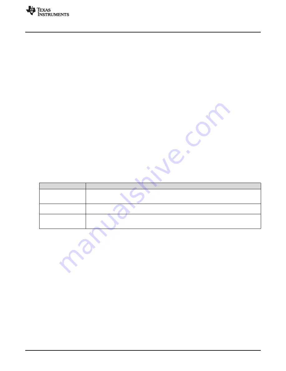
Table 6. Recommended LMK04828 Configurations

Mode

Description

Clock distribution mode

Input reference is distributed to clock outputs and the frequency is divided, if desired. Frequency
multiplication is not supported. Input reference must be provided to CLKin1 input via CLK (J4) and R21
or via EXTREF (J7).

Clock Multiplier Mode

Input reference is locked to internal VCO, allowing frequency integer-N multiplication from input to

(PLL2 Only)

output. Reference must be provided at OSCin input via EXTREF or on-board XO at Y3.

Jitter Cleaner and Clock

Input reference is cleaned with very low bandwidth PLL1 and then multiplied to the desired frequency

Multiplier

using PLL2. Reference must be provided at CLKin1 input or on-board XO at Y1/Y2. On-board VCXO at

Mode (PLL1 + PLL2)

Y3 is also required.

13

SLAU625 – November 2015

ADC14X250EVM Evaluation Module

Submit Documentation Feedback

Copyright © 2015, Texas Instruments Incorporated

Summary of Contents for ADC14X250EVM

Page 1: ...scriptions 14 List of Figures 1 EVM Feature Locations 3 2 Quick Start Test Setup 5 3 HSDC Pro GUI Main Panel 7 4 Data Capture Results from Quick Start Procedure 8 5 ADC14X250EVM GUI 11 6 Low Level View Tab 12 List of Tables 1 Quick Start Performance Measurements 8 2 Troubleshooting Tips 9 3 HSDC Pro Options for Optimal Analysis Results 10 4 ADC14X250 GUI Tab Descriptions 11 5 Low Level View Contro...

Page 2: ...tor 1 1 Required Hardware The following equipment is included in the EVM evaluation kit ADC14X250EVM evaluation board EVM Flying lead to barrel connector power supply cable Mini USB cable The following list of equipment are items that are not included in the EVM evaluation kit but are items required for evaluation of this product to achieve the best performance TSW14J56EVM Kit Data capture board 5...

Page 3: ...and available online See the Section 1 4 section for links High Speed Data Converter Pro software 1 3 Evaluation Board Feature Identification Summary Figure 1 EVM Feature Locations 1 4 References 1 ADC14X250EVM GUI software schematics layout BOM available at www ti com tool adc14x250evm 2 ADC14X250 datasheet available at www ti com product adc14x250 3 LMK04828 datasheet available at www ti com pro...

Page 4: ...250 GUI is used to control the ADC14X250EVM It must be used to properly configured the devices on the EVM 1 Download the GUI from the TI website The Section 1 4 section of this document contains a link to find the software on the TI website 2 Extract the files from the zip file 3 Run setup exe and follow the installation prompts 2 1 2 High Speed Data Converter Pro GUI Installation High Speed Data ...

Page 5: ...x x x x x x x x x x x x x x x x x x x x x x x x x x x x x x x x x x x x x x x x x x 5V 2A www ti com Quick Start Guide 2 2 Hardware Setup Procedure A typical test setup using the ADC14X250EVM and TSW14J56EVM is shown in Figure 2 This is the test setup used for the quick start procedure The rest of this section describes the hardware setup steps Figure 2 Quick Start Test Setup 5 SLAU625 November 20...

Page 6: ...9 3 Connect the 6 dB 50 Ω attenuator to the J3 VIN input 4 Set the analog input signal generator for 70 MHz 10 dBm 5 Connect the analog input signal generator to the VIN input Place the bandpass filter between the analog signal generator and the attenuator input to remove noise and harmonics from the signal generator 6 Set the clock input signal generator for 250 MHz 12 dBm 7 Connect the signal ge...

Page 7: ...OK This popup can be accessed through the Instrument Options menu 3 Select the ADC tab at the top of the GUI 4 Use the Select ADC drop down menu at the top left corner to select ADC14X250_LMF_112 5 When prompted to update the firmware for the ADC click Yes and wait for the firmware to download to the TSW14J56 6 Enter 250M into the ADC Output Data Rate field at the bottom left corner 7 Click the In...

Page 8: ... is not achieved then see the Quick Start Troubleshooting section of this document Figure 4 Data Capture Results from Quick Start Procedure Table 1 Quick Start Performance Measurements Result Measured Value Unit SNR 70 0 dBFS SFDR 85 dBFS 8 ADC14X250EVM Evaluation Module SLAU625 November 2015 Submit Documentation Feedback Copyright 2015 Texas Instruments Incorporated ...

Page 9: ...ice is recognized when the EVM is connected to the PC Device GUI is not Verify that the green USB Status LED light in the top right corner of the GUI is lit If it is not lit press working properly the Reconnect FTDI button Try restarting the configuration GUI Check default jumper connections as shown in Section 6 Verify that the TSW14J56EVM is properly connected to the PC with a mini USB cable and...

Page 10: ...o as a coherent frequency The clock and analog inputs must be frequency locked such as through 10 MHz references in order to achieve coherency If this cannot be achieved then a window function like Blackman must be applied to the data for fast Fourier transform FFT analysis in the HSDC Pro Software 3 3 HSDC Pro Settings The HSDC Pro options highlighted in Table 3 can help improve the performance m...

Page 11: ...X250 Provides controls for ADC14X250 features that can be used to customize evaluation LMK04828 Provides controls for LMK04828 features that can be used to customize evaluation or setup more advanced clocking schemes Low Level View Allows write and read access to all device registers and bits Also allows loading and saving of configuration files The device configurations can be saved from this tab...

Page 12: ...e All Button Update all registers shown in the Register Map with the values shown in the Register Map summary Read Register Button Read from the register highlighted in the Register Map and display the results in the Value column Read All Button Read from all registers in the Register Map and display current state of hardware Also updates the controls in the other tabs Load Config Button Load a Co...

Page 13: ... LMK04828 must be provided via the EXTREF input connector J7 5 1 2 Recommended LMK04828 Configurations The LMK04828 can be used in a number of useful configurations to provide the necessary clocks for the ADC and JESD204B interface as described in Table 6 Table 6 Recommended LMK04828 Configurations Mode Description Clock distribution mode Input reference is distributed to clock outputs and the fre...

Page 14: ...s and their functions are described in Table 8 Table 8 Connector Descriptions Connector Description J1 5V IN 5 V power connector J2 VIN VIN analog input to ADC via transformer network Grounded by default J3 VIN VIN analog input to ADC via transformer network J4 CLK Sampling Clock input for ADC via transformer network J5 SYSREF SYSREF input for ADC via transformer network J6 REFCLK Optional referen...

Page 15: ...ring the warranty period to the address designated by TI and that are determined by TI not to conform to such warranty If TI elects to repair or replace such EVM TI shall have a reasonable time to repair such EVM or provide replacements Repaired EVMs shall be warranted for the remainder of the original warranty period Replaced EVMs shall be warranted for a new full ninety 90 day warranty period 3 ...

Page 16: ... by Industry Canada to operate with the antenna types listed in the user guide with the maximum permissible gain and required antenna impedance for each antenna type indicated Antenna types not included in this list having a gain greater than the maximum gain indicated for that type are strictly prohibited for use with this device Concernant les EVMs avec antennes détachables Conformément à la rég...

Page 17: ... connecting any load to the EVM output If there is uncertainty as to the load specification please contact a TI field representative During normal operation even with the inputs and outputs kept within the specified allowable ranges some circuit components may have elevated case temperatures These components include but are not limited to linear regulators switching transistors pass transistors cu...

Page 18: ...F REMOVAL OR REINSTALLATION ANCILLARY COSTS TO THE PROCUREMENT OF SUBSTITUTE GOODS OR SERVICES RETESTING OUTSIDE COMPUTER TIME LABOR COSTS LOSS OF GOODWILL LOSS OF PROFITS LOSS OF SAVINGS LOSS OF USE LOSS OF DATA OR BUSINESS INTERRUPTION NO CLAIM SUIT OR ACTION SHALL BE BROUGHT AGAINST TI MORE THAN ONE YEAR AFTER THE RELATED CAUSE OF ACTION HAS OCCURRED 8 2 Specific Limitations IN NO EVENT SHALL T...

Page 19: ...esponsible for compliance with all legal regulatory and safety related requirements concerning its products and any use of TI components in its applications notwithstanding any applications related information or support that may be provided by TI Buyer represents and agrees that it has all the necessary expertise to create and implement safeguards which anticipate dangerous consequences of failur...

Reviews: