background image


TCP201 User Manual Issue 1.4 

Page 20 of 35 


3.5  Big / Little Endian Mode setting 

The PCI target chip of the TCP201, the PCI9030 can be set to convert to Big Endian data ordering 
on the local bus. This is useful for IP modules that use Big Endian byte ordering. Big Endian byte 
ordering is the convention used in the Motorola 68000 microprocessor family and is the VMEbus 
convention. 

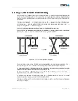
Changing Local Space 0, 1 or 2 to Big Endian mode results in swapped data lines of the local bus:  

A 32 bit access is separated by the PCI9030 into two local 16 bit accesses. Byte lane 0 and 1 are 
swapped, and byte lane 2 and 3 are swapped. 

During 16 bit access, the upper and lower bytes are displayed in reverse order. 

During 8 bit access odd and even addresses are swapped. To access Address 0x00, the Address 
0x01 must be used. An access to Address 0x01 is done by Address 0x00. 


Figure 3-8 :  PCI to Local Byte lane swapping 


The local Endian mode of the PCI9030 can be changed for each local space separately. This is 
done by changing the value of bit 24 in the corresponding Bus Region Descriptor Register: 

To change local Space 0, that provides access to the local control and status registers, from Little 
Endian to Big Endian mode, write 0xD5 to PCI BAR0 + 0x2B. 

To change local Space 1, that provides access to IP I/O- ID and INT- Space, from Little Endian to 
Big Endian mode, write 0x15 to PCI BAR0 + 0x2F. 

To change local Space 2, that provides access to the IP MEM-Space (16 bit port), from Little 
Endian to Big Endian mode, write 0x15 to PCI BAR0 + 0x33. 

Changing local Space 3 from Little Endian to Big Endian mode has no effect, because this space 
has only an 8 bit port. 


Summary of Contents for TCP201

Page 1: ...2006 TEWS TECHNOLOGIES GmbH TEWS TECHNOLOGIES LLC Am Bahnhof 7 25469 Halstenbek Germany www tews com Phone 49 0 4101 4058 0 Fax 49 0 4101 4058 19 e mail info tews com 9190 Double Diamond Parkway Suite 127 Reno NV 89521 USA www tews com Phone 1 775 850 5830 Fax 1 775 201 0347 e mail usasales tews com ...

Page 2: ...oduct described in this document at any time without notice TEWS TECHNOLOGIES GmbH is not liable for any damage arising out of the application or use of the device described herein Style Conventions Hexadecimal characters are specified with prefix 0x i e 0x029E that means hexadecimal value 029E For signals on hardware products an Active Low is represented by the signal name with following i e IP_R...

Page 3: ... Description Date 1 0 Initial Issue October 2002 1 1 Corrections in Chapter Endian Conventions November 2002 1 2 General Revision March 2003 1 3 Correction Figure PCI to Local Byte lane swapping November 2003 1 4 New address TEWS LLC September 2006 ...

Page 4: ...werPC CPU View 17 3 4 3 Intel CPU View with TCP201 switched to Big Endian 18 3 4 4 PowerPC CPU View with TCP201 switched to Big Endian 19 3 5 Big Little Endian Mode setting 20 4 IP INTERFACE 21 4 1 PCI9030 Local Space Assignment 21 4 1 1 Local Space 0 Address Map 22 4 1 2 Local Space 1 Address Map 22 4 1 3 Local Space 2 Address Map 23 4 1 4 Local Space 3 Address Map 24 4 2 IP Interface Register 24...

Page 5: ...AP 22 FIGURE 4 3 LOCAL SPACE 1 ADDRESS MAP IP A D ID INT I O SPACE 22 FIGURE 4 4 LOCAL SPACE 2 ADDRESS MAP IP A D MEMORY SPACE 16 BIT 23 FIGURE 4 5 LOCAL SPACE 3 ADDRESS MAP IP A D MEMORY SPACE 8 BIT 24 FIGURE 4 6 REVISION ID REGISTER PCI BASE ADDRESS 2 0X00 24 FIGURE 4 7 IP A CONTROL REGISTER PCI BASE ADDRESS 2 0X02 25 FIGURE 4 8 IP B CONTROL REGISTER PCI BASE ADDRESS 2 0X04 26 FIGURE 4 9 IP C CO...

Page 6: ... lines Status indicators for IP access 5V and 12V are provided in the front panel The TCP201 can operate with 3 3V and 5 0V PCI I O signaling voltage All IP interrupt request lines are mapped to PCI INTA For fast interrupt source detection the TCP201 provides a special IP Interrupt Status Register IP clock is selectable between 8 MHz and 32 MHz for each IP separately Two memory spaces are provided...

Page 7: ...P interrupts are mapped to PCI INTA Local Interrupt Status Register I O Access HD50 SCSI 2 type connector AMP 787395 5 per IP front panel I O DMA 32 Bit Access Not supported Not supported Status LEDs ACK LED for each IP slot 5V Power LED for each IP slot 12V and 12V Power LED Protection Self healing fuses and RF filtering on all IP power lines Power Requirements without IP Modules 280mA typical 5V...

Page 8: ...ology is used as PCI target device for accessing the IP interface A FPGA is used on the PCI9030 local bus to build the IP interface and provide IP interface control registers The PCI9030 provides four local spaces 0 3 that are used for the IP interface Basic PCI9030 register configuration is loaded from a serial EEPROM after power up or board reset ...

Page 9: ... PCI Base Address 3 for Local Address Space 1 Y FFFFFC00 0x20 PCI Base Address 4 for Local Address Space 2 Y FE000000 0x24 PCI Base Address 5 for Local Address Space 3 Y FF000000 0x28 Cardbus CIS Pointer N 00000000 0x2C Subsystem ID Subsystem Vendor ID N 200A 1498 0x30 PCI Base Address for Local Expansion ROM Y 00000000 0x34 Reserved Next Cap P N 000000 40 0x38 Reserved N 00000000 0x3C Max_Lat Min...

Page 10: ...then reading back the value of the PCI Base Address Register The PCI9030 PCI Target chip returns zero 0 in don t care address bits specifying the required address space The PCI software then maps the local address space into the PCI address space by programming the PCI Base Address Register After programming the required address spaces the user must set bit 0 enables I O accesses and bit 1 enables...

Page 11: ...e Address Implementation 1 Write a value of 1 to all bits of the PCI Base Address Registers 0 to 5 2 Check that bit 0 of the register contains a value of 0 PCI9030 needs a memory address space 3 Starting at bit location 4 of the PCI Base Address Register search for the first bit set to a value of 1 This bit is the binary size of the total contiguous block of memory address space needed by the PCI9...

Page 12: ...dress space needed by the PCI9030 For example if bit 16 of the PCI Base Address Local Expansion ROM Register is detected as the first bit set the device is requesting a 64 kilobyte block of memory address space 7 Write the start address of the requested memory address block to the PCI Base Address Local Expansion ROM Register This memory address region must not conflict with any other memory space...

Page 13: ...00000001 Enabled 0x20 Local Re map Register Space 3 0x02000001 Enabled 0x24 Local Re map Register ROM 0x00000000 Not used 0x28 Local Address Space 0 Descriptor 0xD44160A0 Timing local Space 0 0x2C Local Address Space 1 Descriptor 0x144120A2 Timing local Space 1 0x30 Local Address Space 2 Descriptor 0x144120A2 Timing local Space 2 0x34 Local Address Space 3 Descriptor 0x140120A2 Timing local Space ...

Page 14: ... 0x0001 0x40 0x0400 0x0001 0x0000 0x0001 0x0200 0x0001 0x0000 0x0000 0x50 0xD441 0x60A0 0x1441 0x20A2 0x1441 0x20A2 0x1401 0x20A2 0x60 0x0000 0x0000 0x0800 0x0081 0x0400 0x0201 0x0100 0x0001 0x70 0x0280 0x0001 0x0000 0x0041 0x007A 0x4000 0x0224 0x9252 0x80 0x0000 0x0000 0x0000 0x0000 0xFFFF 0xFFFF 0xFFFF 0xFFFF 0x90 0xFFFF 0xFFFF 0xFFFF 0xFFFF 0xFFFF 0xFFFF 0xFFFF 0xFFFF 0xA0 0xFFFF 0xFFFF 0xFFFF ...

Page 15: ... D23 D16 D15 D8 D7 D0 LSB Big Endian convention on a 32 bit Data Bus Byte Lane Byte 0 Byte 1 Byte 2 Byte 3 Data Line D31 D24 D23 D16 D15 D8 D7 D0 LSB The PCI Bus and all Intel CPUs work in Little Endian mode VMEbus PowerPC and 68K CPUs work in Big Endian mode Most IP modules which are common in VMEbus systems also use Big Endian byte ordering The TCP201 works in Little Endian mode by default but c...

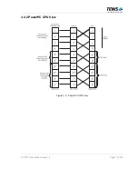
Page 16: ...TCP201 User Manual Issue 1 4 Page 16 of 35 3 4 1 Intel CPU View Figure 3 4 Intel CPU View ...

Page 17: ...TCP201 User Manual Issue 1 4 Page 17 of 35 3 4 2 PowerPC CPU View Figure 3 5 PowerPC CPU View ...

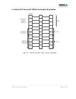
Page 18: ...TCP201 User Manual Issue 1 4 Page 18 of 35 3 4 3 Intel CPU View with TCP201 switched to Big Endian Figure 3 6 Intel CPU View with TCP201 switched to Big Endian ...

Page 19: ...TCP201 User Manual Issue 1 4 Page 19 of 35 3 4 4 PowerPC CPU View with TCP201 switched to Big Endian Figure 3 7 PowerPC CPU View with TCP201 switched to Big Endian ...

Page 20: ...dd and even addresses are swapped To access Address 0x00 the Address 0x01 must be used An access to Address 0x01 is done by Address 0x00 Figure 3 8 PCI to Local Byte lane swapping The local Endian mode of the PCI9030 can be changed for each local space separately This is done by changing the value of bit 24 in the corresponding Bus Region Descriptor Register To change local Space 0 that provides a...

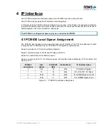
Page 21: ...0 Local Space Assignment The PCI9030 local spaces must be used to access the IP Interface The PCI base address for each local space can be obtained from the PCI9030 PCI configuration register space Space 0 contains the IP Control and Status Register Space 1 provides access to I O ID and INT Space of all IPs Space 2 is used for the IP A D Memory space Space 3 is also used for IP A D Memory space bu...

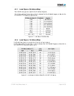
Page 22: ...r the IP A D ID INT and I O space The PCI base address for local space 1 can be obtained from the PCIBAR3 Register at offset 0x1C in the PCI9030 PCI configuration register space PCI Base Address 3 Start End Size Byte Description 0x0000_0000 0x0000_007F 128 IP A I O Space 0x0000_0080 0x0000_00BF 64 IP A ID Space 0x0000_00C0 0x0000_00FF 64 IP A INT Space 0x0000_0100 0x0000_017F 128 IP B I O Space 0x...

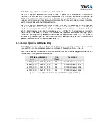
Page 23: ...wledge cycle for IP INT1 The read access returns the interrupt vector This feature is helpful for IP modules that require an interrupt acknowledge cycle to remove their pending interrupt request If the IP does not support write access to its INT space no ACK will be generated by the IP and a local timeout will terminate the cycle after a timeout time of 8µs and the timeout bit is set in the IP Sta...

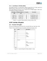
Page 24: ...F_FFFF 4M IP A MEM Space 8 bit 0x0040_0000 0x007F_FFFF 4M IP B MEM Space 8 bit 0x0080_0000 0x00BF_FFFF 4M IP C MEM Space 8 bit 0x00C0_0000 0x00FF_FFFF 4M IP D MEM Space 8 bit Figure 4 5 Local Space 3 Address Map IP A D Memory Space 8 bit 4 2 IP Interface Register 4 2 1 Revision ID Register The Revision ID Register shows the revision of the on board IP FPGA logic Initial Value is 0x00 Changes in th...

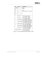
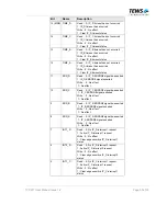
Page 25: ...rresponding IP timeout status bit in the IP Status Register If IP recover time is enabled for an IP slot an IP cycle for this slot will not begin until the IP recover time is expired The IP recover time is app 1µs IP clock rate can be selected between 8 MHz and 32 MHz for each IP separately After power up or board reset the clock rate is set to 8 MHz for all IPs Bit Name Description 15 MSB 14 13 1...

Page 26: ... IP B interrupt 1 level sensitive 1 IP B interrupt 1 edge sensitive 4 INT0_SENSE 0 IP B interrupt 0 level sensitive 1 IP B interrupt 0 edge sensitive 3 ERR_INT_EN 0 IP B error interrupt disabled 1 IP B error interrupt enabled 2 TIME_INT_EN 0 IP B timeout interrupt disabled 1 IP B timeout interrupt enabled 1 RECOVER 0 IP B recover time disabled 1 IP B recover time enabled 0 LSB CLKRATE 0 IP B clock...

Page 27: ... IP C interrupt 1 level sensitive 1 IP C interrupt 1 edge sensitive 4 INT0_SENSE 0 IP C interrupt 0 level sensitive 1 IP C interrupt 0 edge sensitive 3 ERR_INT_EN 0 IP C error interrupt disabled 1 IP C error interrupt enabled 2 TIME_INT_EN 0 IP C timeout interrupt disabled 1 IP C timeout interrupt enabled 1 RECOVER 0 IP C recover time disabled 1 IP C recover time enabled 0 LSB CLKRATE 0 IP C clock...

Page 28: ...IP D interrupt 1 level sensitive 1 IP D interrupt 1 edge sensitive 4 INT0_SENSE 0 IP D interrupt 0 level sensitive 1 IP D interrupt 0 edge sensitive 3 ERR_INT_EN 0 IP D error interrupt disabled 1 IP D error interrupt enabled 2 TIME_INT_EN 0 IP D timeout interrupt disabled 1 IP D timeout interrupt enabled 1 RECOVER 0 IP D recover time disabled 1 IP D recover time enabled 0 LSB CLKRATE 0 IP D clock ...

Page 29: ...ic negation after 200 ms Figure 4 11 IP Reset Register PCI Base Address 2 0x0A 4 2 4 IP Status Register The IP Status Register can be used to read IP timeout error and interrupt status An IP timeout occurs if the IP module fails to generate the IP ACK signal within the IP timeout time The IP timeout time is app 8µs An IP timeout is not reported to the PCI9030 or the PCI master but in the IP Status...

Page 30: ...1 IP_D ERROR signal asserted Write 0 No effect 1 No effect 10 ERR_C Read 0 IP_C ERROR signal de asserted 1 IP_C ERROR signal asserted Write 0 No effect 1 No effect 9 ERR_B Read 0 IP_B ERROR signal de asserted 1 IP_B ERROR signal asserted Write 0 No effect 1 No effect 8 ERR_A Read 0 IP_A ERROR signal de asserted 1 IP_A ERROR signal asserted Write 0 No effect 1 No effect 7 INT1_D Read 0 No IP_D inte...

Page 31: ... IP Interrupts All IP interface interrupt sources Timeout Error IP A D INT0 IP A D INT1 are mapped to PCI interrupt INTA For quick interrupt source detection the IP Status Register can be read to determine the IP interrupt source Level sensitive IP interrupts which are most common for IP modules are cleared by either an interrupt acknowledge cycle to the IP or by accessing an Interrupt Status Regi...

Page 32: ...ine of the IP logic interface which may be used as an optional input to or output from an IP module It is reserved for a digital strobe or clock signal related to the functionality of the IP Strobe signals of all IP slots are accessible on the TCP201 via a 4 pin jumper field Figure 5 1 IP Strobe Signal ...

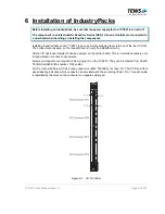
Page 33: ...ctors are keyed so the IndustryPack can only be installed correctly After an IP has been installed it can be secured on the carrier board This is normally necessary only in high vibration or shock environments Screws and spacers are required to fix a single IP on the TCP201 They can be ordered from TEWS TECHNOLOGIES Part number TIPxxx HK All IPs mate with 50 pin SCSI 2 type connectors AMP 787395 5...

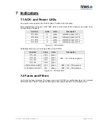
Page 34: ...ates access to IP C IP D ACK D green Indicates access to IP D Figure 7 1 IP ACK LED Additionally there are 6 green Power LEDs on the TCP201 Function Label Color Description IP A 5V 5V A green IP B 5V 5V B green IP C 5V 5V C green IP D 5V 5V D green LED on IP power supply ok 12V common to all IP 12V green LED on 12V power ok 12V common to all IP 12V green LED on 12V power ok Figure 7 2 IP Power LED...

Page 35: ... 31 MemSel 7 D3 8 D4 32 DMAReq1 33 IntSel 9 D5 10 D6 34 DMAck 35 IOSel 11 D7 12 D8 36 Reserved 37 A1 13 D9 14 D10 38 DMAEnd 39 A2 15 D11 16 D12 40 Error 41 A3 17 D13 18 D14 42 IntReq0 43 A4 19 D15 20 BS0 44 IntReq1 45 A5 21 BS1 22 12V 46 Strobe 47 A6 23 12V 24 5V 48 ACK 49 Reserved 25 GND 50 GND Figure 8 1 IP J1 Logic Interface Pin Assignment The IP J2 I O connector routes the IP I O lines directl...

Reviews: