S50 Hardware User Guide
1VV0301505 Rev. 3
Page 31 of 60
2021-05-05
Not Subject to NDA
6.
ELECTRICAL CHARACTERISTICS
6.1.
Absolute Maximum Ratings
Stresses beyond those listed under “Absolute Maximum Ratings” may cause permanent
damage to the device. These are stress ratings only and functional operation of the device
at these or any other condition
s beyond those indicated under “Electrical Requirements”
is not implied. Exposure to absolute-maximum-rated conditions for extended periods
may affect device reliability.
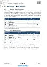
Symbol
Item
Condition
Limit
Unit
Min
Typ
Max
VSUP
Supply voltage
-0,3
3,6
V
V
Pin
Voltage on any pin
-0,3
VSUP+0,3
≤
3,6
V
P
RFin
RF input level
10
dBm
I
NFC1/2
NFC antenna pin current
80
mA
T
stg
Storage temperature range
-40
+125
°C
Table 10: Absolute Maximum Ratings
6.2.
Operating Conditions
Symbol
Item
Condition
Limit
Unit
Min
Typ
Max
VSUP
Supply voltage
DC/DC not enabled
1,7
3,0
3,6
V
DC
DC/DC enabled
1,7
3,0
3,6
V
DC
t
Vrise
Supply rise time
0V to 1,7V
60
ms
T
op
Operating temperature
range
-40
+85
°C
Table 11 Operating Conditions
6.3.
DC Parameter
All Module I/O pins are connected directly to the Nordic nRF52832 chip without signal
conditioning except for some pull-up/pull-down resistors (as indicated). Therefore, the
electrical characteristics are as documented in the Nordic nRF52832 data sheet [7].

