background image

Telink FR1 PCB Design Guideline 

AN-22051900-E1                                                                                      Ver. 1.0.0 

18 

5.


Routing Notes 

Please be noted of the following routing points. 


Prioritize the power and RF circuit routings, power wires should be as thick as possible (0.5mm ~ 1mm), 

as close as possible to the power supply components or chip end in the use of star alignment 

respectively power supply. 


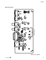
Then comes the normal routing, prioritize to route audio lines, and audio lines should have complete 

copper on both sides, as shown in Figure 5-1. 


For via hole, carbon film hole is needed, pay attention that put the carbon film hole as far as possible 

with the routing and other carbon film hole, at least 1mm, to prevent short circuit. 


Keep the width of the carbon film routing at 1mm or more to reduce carbon film impedance.   


The ground is the main focus for FR1 board design. 


Due to the high current jumps during RF operation, the smaller the GND impedance, the better, to 

help reduce RF noise. For single-layer board, we should connect each component's ground with 

wires after the power routing is completed, giving priority to ensuring that the ground line can go 

through, and adding the 0R cross-line resistor at locations where it has blocks. 


Ground wire should be as thick as 1mm and above, and routed in a ground shape. 


Routing does not require excessive division of the ground plane, that is, the same direction routing 

is together, and the routing distance should not be too long to affect the ground backflow. Priority 

to ensure that the chip center ground and the power supply negative ground has a good ground 

connection. 


The crystal should be grounded as much as possible, and the RF components should be completely 

grounded and covered with solid copper, as shown in Figure 5-1. 


Avoid large areas of solid copper, in the wave soldering process, abnormal heat dissipation, the board is 

easy to bulge. When encountering large areas of copper coverage, choose a mesh structure to facilitate 

heat dissipation. For key circuits, such as RF, crystal, audio lines, and etc., the complete copper coverage 

can be used directly. In addition, for some areas of narrow space, the complete copper should be laid out 

to strengthen the ground reflow, as shown in Figure 5-1. 


Summary of Contents for FR1

Page 1: ...Telink FR1 PCB Design Guideline AN 22051900 E1 Ver 1 0 0 2022 05 19 Keyword Layout FR1 PCB Brief This is Telink FR1 PCB design guideline which mainly introduces considerations when designing FR1 boards ...

Page 2: ...document or any products herein This document may contain technical inaccuracies or typographical errors Telink Semiconductor disclaims any and all liability for any errors inaccuracies or incompleteness contained herein Copyright 2022 Telink Semiconductor Shanghai Co Ltd Information For further information on the technology product and business term please contact Telink Semiconductor Company www...

Page 3: ...Telink FR1 PCB Design Guideline AN 22051900 E1 Ver 1 0 0 3 Revision History Version Change Description Date Author V1 0 0 Initial release 2022 05 Junyao MAO Weixiang WANG ...

Page 4: ...lbe layer board 8 2 2 1 Component and copper wire layer carbon film alignment layer 8 2 2 2 Component and copper wire layer carbon film and copper wire layer 9 3 Key Points of FR1 Board Design 10 3 1 Board layer 10 3 1 1 Board thickness selection 10 3 1 2 Introduction of board structure 10 3 2 Carbon film routing 11 4 Layout Regulations 13 4 1 Package 13 4 2 Solder pads and vias 13 4 3 Notes 15 5 ...

Page 5: ...r routing carbon film routing 9 Figure 3 1 Stack structure 10 Figure 3 2 Carbon film routing 12 Figure 4 1 Package forms 13 Figure 4 2 Package design for Telink IC 14 Figure 4 3 Via hole on carbon film 15 Figure 4 4 Layout for RF circuit 16 Figure 4 5 Layout for power capacitors 17 Figure 5 1 Routing example 1 19 Figure 5 2 Routing example 2 19 Figure 5 3 Routing example 3 20 ...

Page 6: ...cost concern PCB designs are increasingly preferred to use FR1 boards single layer boards which leads to more obvious problems in wireless communication including power interference RF high harmonics and etc This document uses the Telink SoC chips as a basis and the remote control design as an example to illustrate how to guide the design of FR1 boards to achieve fast development and avoid multipl...

Page 7: ...chips can be divided into single layer boards or double layer boards 2 1 Single layer board In single layer board design make sure that all components and keys can be placed on the same side and there should be enough space for the PCB antenna This is suitable for boards with a small number of components and routings The remote control board shown below can be designed as a single layer board Figu...

Page 8: ...is for carbon film routing For example in a remote control design we place the components on one layer and the keys on the other layer The keys need to be designed as carbon film keys and the keys routing is connected to the component layer via carbon film via holes Note that carbon film vias are chosen for cost concerns The remote control board shown below can be designed as this type of double l...

Page 9: ...he keys need to be designed as carbon film keys and the keys routing is connected to the component layer via carbon film via holes When there are many components and the routing is complex if the design shown in 2 2 1 cannot be completed routing then in addition to the carbon film routing on another layer it is necessary to add copper routing and connect the component side routing through the carb...

Page 10: ...be 1 2mm or 1 0mm Note 1 CEM 1 is more suitable for making thinner boards than FR1 and CEM 1 is less likely to warp boards than FR1 over wave soldering 2 Whether FR1 or CEM 1 is used the rules and notes for PCB design are the same 3 1 2 Introduction of board structure In general FR1 circuit board is single surface board however we need create another layer in addition to the Top layer and Bottom l...

Page 11: ...il on one side 0 05mm 113 Diameter of insulated opening 1 6mm 0 1mm greater than copper plate on one side when insulated 114 Diameter of the carbon film on the surface of the grouting hole 1 8mm When there is no protective oil in principle the carbon film is required to be 0 2mm larger on one side of the copper plate to avoid revealing copper When it is not possible to meet the carbon film single ...

Page 12: ...and the edge of the green oil covered wire 0 5mm The principle is to avoid short circuits caused by carbon oil seepage in case of pinholes in the single layer of green oil the edge of the carbon plate is at least 0 1mm from the insulation layer covering the wire when there is an insulation layer underneath the carbon film 121 Carbon hole resistance 100 ohms hole 122 Carbon hole reliability design ...

Page 13: ... MIC are shown in the figure below Figure 4 1 Package forms 4 2 Solder pads and via holes The PCB package design of Telink IC is as shown in Figure 4 2 The carbon film via hole is shown in Figure 4 3 the hole diameter is greater than 0 7mm outer diameter 1 4mm The air gap between carbon film hole and copper wire is 2 5mm or more ...

Page 14: ...Telink FR1 PCB Design Guideline AN 22051900 E1 Ver 1 0 0 14 Figure 4 2 Package design for Telink IC ...

Page 15: ...omponents in the location column area The components used for RF matching are close to the RF pins The ANT circuit is isolated from the chip and other circuits by ground to avoid signal crosstalk The capacitors of the LC filter are placed on both sides of the RF routing as shown in Figure 4 4 The purpose of placing on both sides of the RF routing is to allow better harmonic regulation It is best t...

Page 16: ...must be filtered through a capacitor The power supply route is the positive end of the battery spring tab the filter capacitor the power pin of the chip The filter capacitor for the chip s power pin should be placed as close as possible to the corresponding pin of the chip Figure 4 4 Layout for RF circuit ...

Page 17: ...Telink FR1 PCB Design Guideline AN 22051900 E1 Ver 1 0 0 17 Figure 4 5 Layout for power capacitors ...

Page 18: ...und with wires after the power routing is completed giving priority to ensuring that the ground line can go through and adding the 0R cross line resistor at locations where it has blocks Ground wire should be as thick as 1mm and above and routed in a ground shape Routing does not require excessive division of the ground plane that is the same direction routing is together and the routing distance ...

Page 19: ...ting example 1 In order to make a good connection between the chip and the ground and improve the RF performance it can be connected to the system ground through the chip s four corner ground as shown in the location of the red arrow in Figure 5 2 Figure 5 2 Routing example 2 ...

Page 20: ...plete for the copper plates where the ground plane is disconnected from the chip ground or power ground due to the routing we should use 1206 package resistor to across the line to make it connected with the chip ground or power ground copper as shown in Figure 5 3 Figure 5 3 Routing example 3 ...

Reviews: